

Datasheet M48Z128Y, M48Z128-85PM1, M48Z128-70PM1, M48Z128-120PM1, M48Z128 Datasheet (SGS Thomson Microelectronics)
...Page 1

1 Mbit (128Kb x8) ZEROPOWERSRAM
■ INTEGRATED LOW POWER SRAM,
POWER-FAIL CONTROL CIRCUIT and
BATTERY
■ CONVENTIONAL SRAM OPERATION;
UNLIMITED WRITE CYCLES
■ 10 YEARS of DATA RETENTION inthe
ABSENCE of POWER
■ AUTOMATIC POWER-FAIL CHIP DESELECT
and WRITE PROTECTION
■ WRITE PROTECT VOLTAGES
(V
= Power-fail Deselect Voltage):
PFD
– M48Z128: 4.50V ≤ V
– M48Z128Y: 4.20V ≤ V
■ BATTERY INTERNALLY ISOLATED UNTIL
POWER IS APPLIED
■ PIN and FUNCTION COMPATIBLE with
JEDEC STANDARD 128K x8 SRAMs
■ SURFACE MOUNT CHIP SET PACKAGING
INCLUDES a 28-PIN SOIC and a 32-LEAD
TSOP (SNAPHAT TOP TO BE ORDERED
SEPARATELY)
■ SOIC PACKAGE PROVIDES DIRECT
CONNECTION for a SNAPHAT TOP WHICH
CONTAINS the BATTERY
■ SNAPHAT
HOUSING (BATTERY) IS
REPLACEABLE
PFD
PFD
≤ 4.75V
≤ 4.50V
32
1
PMDIP32 (PM)
Module
TSOP32
(8 x 20mm)
Surface Mount Chip Set Solution (CS)
Figure 1. Logic Diagram
V
CC
M48Z128
M48Z128Y
SNAPHAT (SH)
Battery
SOH28
Table 1. Signal Names
A0-A16 Address Inputs
DQ0-DQ7 Data Inputs / Outputs
E Chip Enable
G Output Enable
W Write Enable
V
CC
V
SS
NC Not Connected Internally
Supply Voltage
Ground
A0-A16
W
17
M48Z128
M48Z128Y
E
G
V
SS
8
DQ0-DQ7
AI01194
1/17June 2000
Page 2
M48Z128, M48Z128Y
Table 2. Absolute Maximum Ratings
Symbol Parameter Value Unit
T
A
T
STG
T
BIAS
(2)
T
SLD
V
IO
V
CC
Note: 1. Stresses greater than those listed under ”Absolute Maximum Ratings” may cause permanent damage to thedevice. This is astress
rating only and functional operation of the device at these or any other conditions above those indicated in the operational section
of this specification is not implied. Exposure to the absolute maximum rating conditions for extended periods of time may affect
reliability.
2. Soldering temperature not to exceed 260°C for 10 seconds (total thermal budget not to exceed 150°C for longer than 30 seconds).
CAUTION: Negative undershoots below –0.3V are not allowed on any pin while in the Battery Back-up mode.
Ambient Operating Temperature 0 to 70 °C
Storage Temperature(VCCOff)
Temperature Under Bias –10 to 70 °C
Lead Solder Temperature for 10 seconds 260 °C
Input or Output Voltages –0.3 to 7 V
Supply Voltage –0.3 to 7 V
(1)
–40 to 70 °C
Table 3. Operating Modes
Mode
Deselect
Write
Read
Read V
Deselect
Deselect ≤ V
Note: 1. X = VIHor VIL;VSO= Battery Back-up Switchover Voltage.
V
CC
4.75V to 5.5V
or
4.5V to 5.5V
to V
V
SO
PFD
(min)
SO
E G W DQ0-DQ7 Power
V
IH
V
IL
V
IL
IL
X X X High Z CMOS Standby
X X X High Z Battery Back-up Mode
X X High Z Standby
X
V
IL
V
IH
V
IL
V
IH
V
IH
D
IN
D
OUT
High Z Active
Active
Active
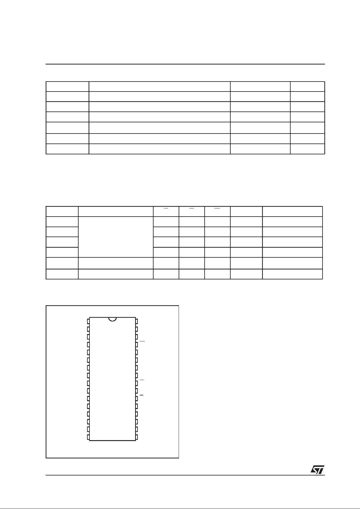
Figure 2. DIP Connections
NC V
1
A16
2
A14
A12
4
A7
5
A6
6
A5
7
A4
A3
A2
A1
A0
DQ0
DQ2
SS
2/17
M48Z128
8
M48Z128Y
9
10
11
12
13
14
15
16
32
31
30
29
28
27
26
25
24
23
22
21
20
19
18
17
AI01195
CC
A15
NC3
W
A13
A8
A9
A11
G
A10
E
DQ7
DQ6
DQ5DQ1
DQ4
DQ3V
DESCRIPTION
The M48Z128/128Y ZEROPOWERRAM is a
128 Kbit x8 non-volatile static RAM thatintegrates
power-fail deselect circuitry and battery control
logic on a single die. The monolithic chip is availablein two special packagesto provide ahighly integrated battery backed-up memory solution.
The M48Z128/128Y is a non-volatile pin andfunction equivalent to any JEDEC standard 128K x8
SRAM. Italso easily fits into many ROM, EPROM,
and EEPROM sockets, providing the non-volatility
of PROMs without any requirement for special
write timing or limitations on the number of writes
that can be performed. The 32 pin 600mil DIP
Module houses the M48Z128/128Y silicon with a
long life lithiumbutton cell in a single package.
Forsurface mountenvironments STprovidesa Chip
Set solution consisting of a 28 pin 330mil SOIC
NVRAMSupervisor (M40Z300) and a 32 pin TSOP
(8x 20mm) LPSRAM (M68Z128) packages.
The 28 pin 330mil SOIC provides sockets with
gold plated contacts at both ends for direct connection to a separate SNAPHAT housing containing the battery.
Page 3
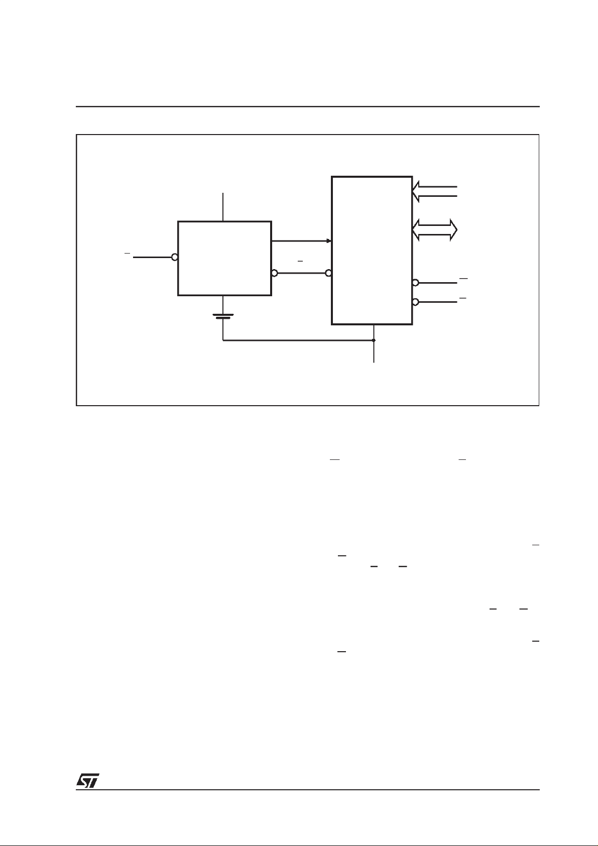
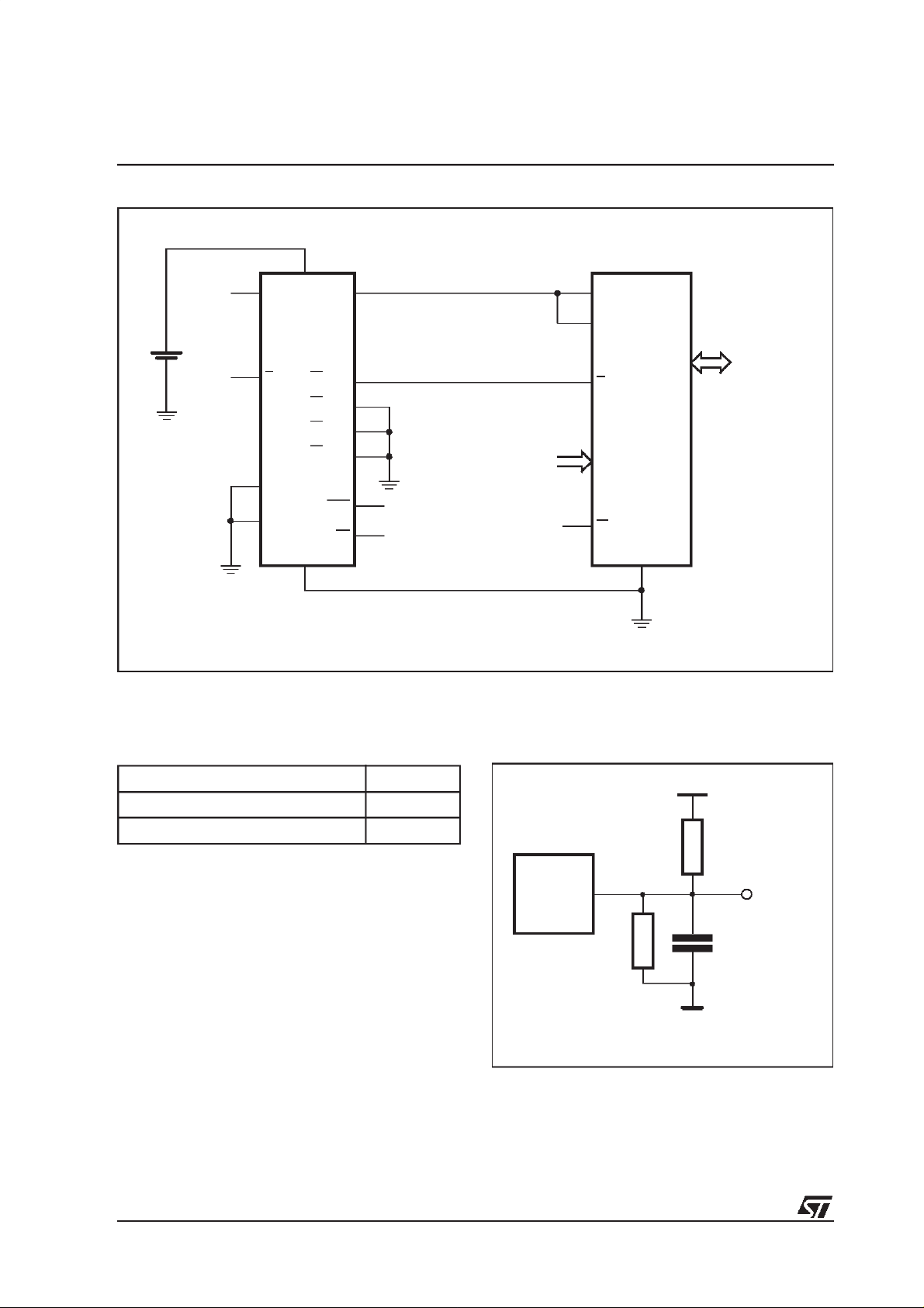
Figure 3. Block Diagram
M48Z128, M48Z128Y
V
CC
A0-A16
POWER
VOLTAGE SENSE
E
AND
SWITCHING
CIRCUITRY
INTERNAL
BATTERY
The unique design allows the SNAPHAT battery
package to be mounted on top of the SOIC package after the completion of the surface mount process. Insertion of the SNAPHAT housing after
reflow prevents potential battery damage due to
the hightemperatures required for device surfacemounting. The SNAPHAT housing is keyed to prevent reverse insertion.
The SNAPHAT battery package is shipped separately in plastic anti-static tubes or in Tape & Reel
form. The part number is ”M4Z28-BRxxSH1”.
The M48Z128/128Y also has its own Power-fail
Detect circuit.The control circuitry constantly monitors the single 5V supply for an out of tolerance
condition. When VCCis out of tolerance, the circuit
write protects the SRAM, providing a high degree
of data security in the midst of unpredictable system operation broughton by low VCC.AsVCCfalls
below approximately 3V, the control circuitry connects the battery which maintains data until valid
power returns.
131,072 x
SRAM ARRAY
E
8
V
SS
DQ0-DQ7
W
G
AI01196
READ MODE
The M48Z128/128Y is in the Read Mode whenever W (Write Enable) is high and E (Chip Enable) is
low. The device architecture allows ripple-through
access of datafrom eight of 1,048,576 locations in
the static storage array. Thus, the unique address
specified by the 17 Address Inputs defines which
oneof the 131,072 bytes of data istobe accessed.
Valid data will be available at the Data I/O pins
within Address Access time (t
) after the last
AVQV
address input signal is stable, providing that the E
and G (Output Enable) access times are also satisfied. If the Eand G access times are notmet, valid data will be available after the later of Chip
Enable Access time (t
cess Time (t
). The state of the eight three-
GLQV
) or Output Enable Ac-
ELQV
state Data I/O signals is controlled by E and G. If
the outputs are activated before t
AVQV
lines will be driven to an indeterminate state until
t
. If the Address Inputs are changed while E
AVQV
and G remain low, output data will remain valid for
Output Data Hold time (t
) but will go indeter-
AXQX
minate until the next Address Access.
, the data
3/17
Page 4
M48Z128, M48Z128Y
Figure 4. Hardware Hookup for SMT Chip Set
(2)
M40Z300
E1
E2
E3
E4
V
SS
V
CON
CON
CON
CON
OUT
RST
BL
SNAPHAT
BATTERY
THS
(3)
E
A
B
(1)
V
CC
E2
M68Z128
E
A0-A16
W
DQ0-DQ7
V
SS
AI03625
Note: 1. For pin connections, see individual data sheets for M40Z300 and M68Z128 at www.st.com.
2. Connect THS pin toV
3. SNAPHAT ordered separately.
Table 4. AC MeasurementConditions
OUT
if 4.2V ≤ V
≤ 4.5V (M48Z128Y) or connect THS pin to VSSif 4.5V ≤ V
PFD
Figure 5. AC Testing Load Circuit
Input Rise and Fall Times ≤ 5ns
Input Pulse Voltages 0 to 3V
Input and Output Timing Ref. Voltages 1.5V
Note that OutputHi-Z is defined as thepoint where datais no longer
driven.
DEVICE
UNDER
TEST
1kΩ
CLincludes JIG capacitance
≤ 4.75V (M48Z128).
PFD
5V
1.9kΩ
CL= 100pF or
OUT
5pF
AI01030
4/17
Page 5
M48Z128, M48Z128Y
Table 5. Capacitance
(1, 2)
(TA=25°C, f = 1MHz)
Symbol Parameter Test Condition Min Max Unit
V
V
IN
OUT
=0V
=0V
10 pF
10 pF
C
IN
C
IO
Note: 1. Effective capacitance measured with power supply at 5V.
2. Sampled only, not 100% tested.
3. Outputs deselected.
Input Capacitance
(3)
Input / Output Capacitance
Table 6. DC Characteristics
(TA= 0 to 70 °C; VCC= 4.75V to 5.5V or 4.5V to 5.5V)
Symbol Parameter Test Condition Min Max Unit
(1)
I
LI
I
LO
I
CC
I
CC1
I
CC2
V
IL
V
IH
V
OL
V
OH
Note: 1. Outputs deselected.
Input Leakage Current
(1)
Output Leakage Current
Supply Current
Supply Current (Standby)TTL
Supply Current (Standby)CMOS E ≥ VCC– 0.2V 4 mA
Input Low Voltage –0.3 0.8 V
Input High Voltage 2.2
Output Low Voltage
Output High Voltage
0V ≤ V
0V ≤ V
E=V
I
OL
I
≤ V
IN
CC
≤ V
OUT
, Outputs open
IL
E=V
IH
= 2.1mA
= –1mA
OH
CC
±1 µA
±1 µA
105 mA
7mA
V
+ 0.3
CC
0.4 V
2.4 V
V
Table 7. Power Down/UpTripPoints DC Characteristics
(1)
(TA= 0 to 70 °C)
Symbol Parameter Min Typ Max Unit
V
PFD
V
SO
t
DR
Note: 1. All voltages referenced to VSS.
2. At 25 °C.
Power-fail Deselect Voltage
Battery Back-up Switchover Voltage 3 V
(2)
Data Retention Time 10 YEARS
M48Z128 4.5 4.6 4.75 V
M48Z128Y 4.2 4.3 4.5 V
5/17
Page 6
M48Z128, M48Z128Y
Table 8. Power Down/Up AC Characteristics
(TA= 0 to 70 °C)
Symbol Parameter Min Max Unit
(1)
t
F
t
FB
t
WP
t
R
V
(max) to V
(2)
PFD
V
(min) to VSOVCCFallTime
PFD
PFD
Write Protect Time from VCC=V
VSOto V
(max) VCCRise Time
PFD
(min) VCCFall Time 300 µs
10 µs
PFD
40 150 µs
0 µs
t
ER
Note: 1. V
2. V
E Recovery Time 40 120 ms
(max) toV
PFD
(min).
es V
PFD
(min) to VSOfall time of less than tFBmay cause corruption of RAM data.
PFD
(min) falltime of less than tFmay result indeselection/write protection not occurring until 200µs after VCCpass-
PFD
Figure 6. Power Down/Up Mode AC Waveforms
V
CC
V
(max)
PFD
V
(min)
PFD
V
SO
tF
tFB
tWP
E
OUTPUTS
VALID VALID
(PER CONTROLINPUT)
tDR
DON’T CARE
HIGH-Z
tR
tER
RECOGNIZEDRECOGNIZED
(PER CONTROLINPUT)
6/17
AI01031
Page 7

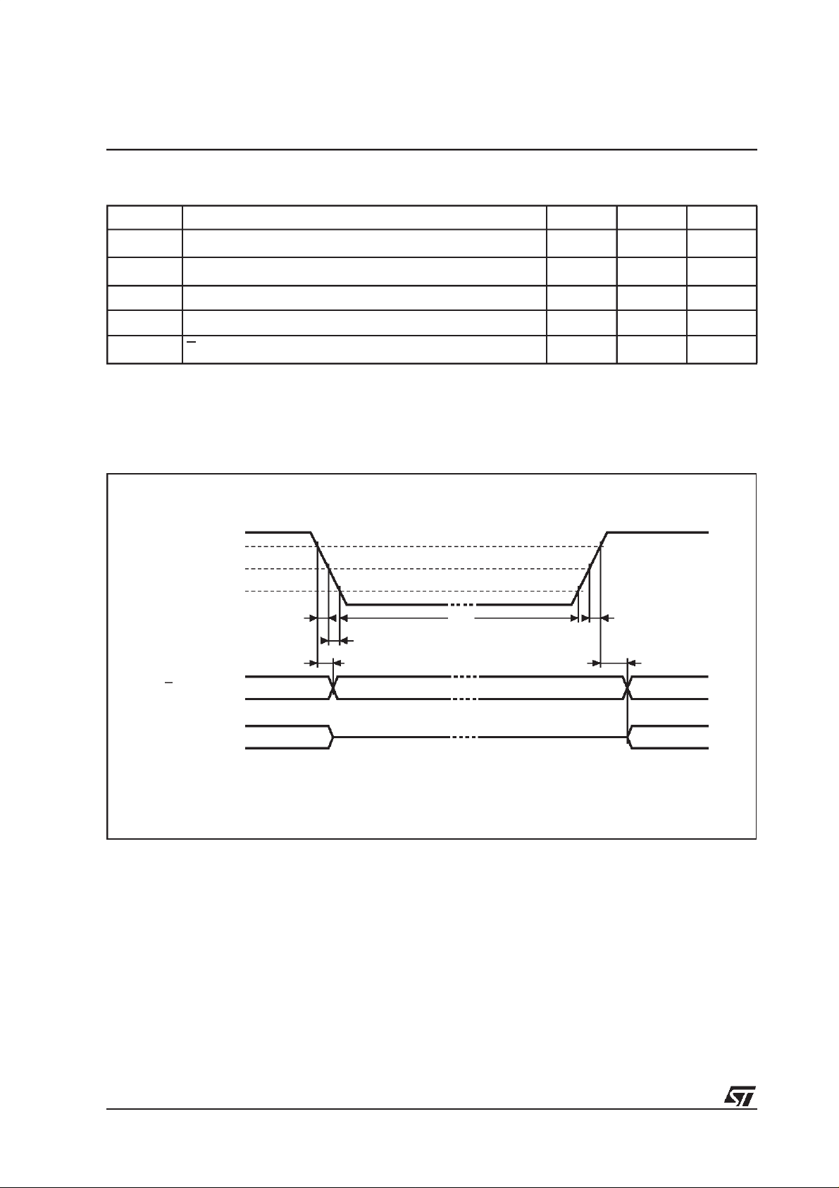
Table 9. Read Mode AC Characteristics
(TA= 0 to 70 °C; VCC= 4.75V to 5.5V or 4.5V to 5.5V)
Symbol Parameter
Min Max Min Max Min Max
t
AVAV
t
AVQV
t
ELQV
t
GLQV
t
ELQX
t
GLQX
t
EHQZ
t
GHQZ
t
AXQX
Note: 1. CL= 100pF.
2. C
Read Cycle Time 70 85 120 ns
(1)
Address Valid to Output Valid 70 85 120 ns
(1)
Chip Enable Low to Output Valid 70 85 120 ns
(1)
Output Enable Low to Output Valid 35 45 60 ns
(2)
Chip Enable Low to Output Transition 5 5 5 ns
(2)
Output Enable Low to Output Transition 3 3 3 ns
(2)
Chip Enable High to Output Hi-Z 30 35 45 ns
(2)
Output Enable High to Output Hi-Z 20 25 35 ns
(1)
Address Transition to Output Transition 5 5 10 ns
= 5pF.
L
M48Z128, M48Z128Y
M48Z128/M48Z128Y
Unit-70 -85 -120
Figure 7. Address Controlled, Read Mode AC Waveforms
tAVAV
A0-A16
tAVQV tAXQX
DQ0-DQ7
Note: Chip Enable (E) and Output Enable (G) = Low, Write Enable (W) = High.
VALID
DATA VALID
AI01078
7/17
Page 8

M48Z128, M48Z128Y
Figure 8. Chip Enable or Output Enable Controlled, Read Mode AC Waveforms
tAVAV
A0-A16
tAVQV tAXQX
tELQV
E
tELQX
tGLQV
G
tGLQX
DQ0-DQ7
Note: Write Enable (W) = High.
WRITE MODE
The M48Z128/128Y is in the Write Modewhenever W and E are active.The start of a write is referenced from thelatter occurring falling edgeof W or
E. A write is terminated by the earlier rising edge
of W or E.
The addresses must be held valid throughout the
cycle. E or W must return high for minimum of t
from E or t
HAX
from W prior to the initiation
WHAX
E-
of anotherread or write cycle. Data-in must bevalid t
for t
prior to the end of write and remain valid
DVWH
WHDX
or t
afterward. G should be kept
EHDX
high during write cycles to avoid bus contention;
although, if the output bus has been activated by a
low on Eand G, a low on Wwill disable the outputs
t
after W falls.
WLQZ
DATA RETENTION MODE
With valid VCCapplied, the M48Z128/128Y operates as a conventional BYTEWIDETMstatic RAM.
Should the supply voltage decay, the RAM will automatically power-fail deselect, write protecting it-
VALID
tEHQZ
tGHQZ
DATA OUT
AI01197
self tWPafter VCCfalls below V
PFD
become high impedance, andall inputs are treated
as ”don’t care.”
If power fail detection occurs during a valid access, the memory cycle continuesto completion. If
the memory cycle fails to terminate within the time
tWP, write protection takes place. When VCCdrops
below VSO, the control circuit switches power to
the internal energy source which preserves data.
The internal coin cell will maintain data in the
M48Z128/128Y after the initial application of V
for an accumulated period of at least 10 years
when VCCis less than VSO. As system power returns and VCCrises above VSO, the battery is disconnected, and the power supply is switched to
external VCC. Write protection continues for tERafter VCCreaches V
to allow for processor stabi-
PFD
lization. After tER, normal RAM operation can
resume.
For more information on Battery Storage Life refer
to the Application Note AN1012.
. All outputs
CC
8/17
Page 9

M48Z128, M48Z128Y
Table 10. Write Mode AC Characteristics
(TA= 0 to 70 °C; VCC= 4.75V to 5.5V or 4.5V to 5.5V)
M48Z128/M48Z128Y
Symbol Parameter
Min Max Min Max Min Max
t
AVAV
t
AVWL
t
AVEL
t
WLWH
t
ELEH
t
WHAX
t
EHAX
t
DVWH
t
DVEH
t
WHDX
t
EHDX
(1, 2)
t
WLQZ
t
AVWH
t
AVEH
(1, 2)
t
WHQX
Note: 1. CL= 5pF.
2. If E goes low simultaneously with W going low after W going low, the outputs remain in the high impedance state.
Write Cycle Time 70 85 120 ns
Address Valid to Write Enable Low 0 0 0 ns
Address Valid to Chip Enable Low 0 0 0 ns
Write Enable Pulse Width 55 65 85 ns
Chip Enable Low to Chip Enable High 55 75 100 ns
Write Enable High to Address Transition 5 5 5 ns
Chip Enable High to Address Transition 15 15 15 ns
Input Valid to Write Enable High 30 35 45 ns
Input Valid to Chip Enable High 30 35 45 ns
Write Enable High to Input Transition 0 0 0 ns
Chip Enable High to Input Transition 10 10 10 ns
Write Enable Low to Output Hi-Z 25 30 40 ns
Address Valid to Write Enable High 65 75 100 ns
Address Valid to Chip Enable High 65 75 100 ns
Write Enable High to Output Transition 5 5 5 ns
Unit-70 -85 -120
POWER SUPPLY DECOUPLING
and UNDERSHOOT PROTECTION
ICCtransients,including those produced by output
switching, can produce voltage fluctuations, resulting in spikes on the VCCbus. These transients
can be reduced if capacitors are used to store energy, which stabilizes the VCCbus. The energy
stored in the bypass capacitors will be released as
low going spikes are generated or energy will be
absorbed when overshoots occur. A ceramic bypass capacitor value of 0.1µF (as shown in Figure
9) is recommended in order to provide the needed
filtering.
In addition to transients that are caused bynormal
SRAM operation,power cyclingcangenerate negative voltage spikes on VCCthat drive it to values
below VSSby as much as one Volt. These negative spikescan cause data corruptioninthe SRAM
while in battery backup mode. To protect from
these voltage spikes, it is recommended to connect a schottky diode from VCCto VSS(cathode
connected to VCC, anode to VSS). Schottky diode
1N5817 is recommended for through hole and
MBRS120T3 is recommended for surface mount.
Figure 9. Supply Voltage Protection
V
CC
V
CC
0.1µF DEVICE
V
SS
AI02169
9/17
Page 10

M48Z128, M48Z128Y
Figure 10. Write Enable Controlled, Write AC Waveforms
A0-A16
tAVEL
E
tAVWL
W
tWLQZ
DQ0-DQ7
Note: Output Enable (G) = High.
tAVAV
VALID
tAVWH
tWLWH
Figure 11. Chip Enable Controlled, Write AC Waveforms
DATA INPUT
tDVWH
tWHAX
tWHQX
tWHDX
AI01198
A0-A16
E
W
DQ0-DQ7
Note: Output Enable (G) = High.
10/17
tAVEL
tAVWL
tAVAV
VALID
tAVEH
tELEH
DATA INPUT
tDVEH
tEHAX
tEHDX
AI01199
Page 11

Table 11. Ordering Information Scheme
Example: M48Z128Y -70 CS 1
Device Type
M48Z
Supply Voltage and Write Protect Voltage
128 = V
128Y = V
= 4.75V to 5.5V; V
CC
= 4.5V to 5.5V; V
CC
Speed
-70 = 70ns
-85 = 85ns
-120 = 120ns
Package
PM = PMDIP32
(1)
= Surface Mount Chip Set solution M40Z300 (SOH28) + M68Z128 (TSOP32)
CS
Temperature Range
1=0to70°C
= 4.5V to 4.75V
PFD
= 4.2V to4.5V
PFD
M48Z128, M48Z128Y
Note: 1. The SOIC package (SOH28) requires the battery package (SNAPHAT) which is ordered separately under the part number
”M4Zxx-BR00SH1” in plastic tube or ”M4Zxx-BR00SH1TR” in Tape & Reel form.
Caution: Donot place the SNAPHAT batterypackage ”M4Zxx-BR00SH1” in conductive foam since this will drain the lithium button-cell
battery.
For a list of available options (Speed, Package, etc...) or for further information on any aspect of this device, please contact the STMicroelectronics Sales Office nearest to you.
Table 12. Revision History
Date Revision Details
May 1999 First Issue
04/13/00
06/20/00
Document Layout changed
Surface Mount Chip Set solution added
t
changed (Table 9)
GLQX
11/17
Page 12

M48Z128, M48Z128Y
Table 13. PMDIP32 - 32 pin Plastic Module DIP, Package Mechanical Data
Symbol
Typ Min Max Typ Min Max
A 9.27 9.52 0.365 0.375
A1 0.38 0.015
B 0.43 0.59 0.017 0.023
C 0.20 0.33 0.008 0.013
D 42.42 43.18 1.670 1.700
E 18.03 18.80 0.710 0.740
e1 2.29 2.79 0.090 0.110
e3 34.29 41.91 1.350 1.650
eA 14.99 16.00 0.590 0.630
L 3.05 3.81 0.120 0.150
S 1.91 2.79 0.075 0.110
N32 32
mm inches
Figure 12. PMDIP32 - 32pin Plastic Module DIP, Package Outline
A1AL
S
Be1
e3
D
N
E
1
Drawing is notto scale.
C
eA
PMDIP
12/17
Page 13

M48Z128, M48Z128Y
Table 14. SOH28 - 28 lead Plastic Small Outline, battery SNAPHAT, Package Mechanical Data
Symbol
Typ Min Max Typ Min Max
A 3.05 0.120
A1 0.05 0.36 0.002 0.014
A2 2.34 2.69 0.092 0.106
B 0.36 0.51 0.014 0.020
C 0.15 0.32 0.006 0.012
D 17.71 18.49 0.697 0.728
E 8.23 8.89 0.324 0.350
e 1.27 – – 0.050 – –
eB 3.20 3.61 0.126 0.142
H 11.51 12.70 0.453 0.500
L 0.41 1.27 0.016 0.050
α 0° 8° 0° 8°
N28 28
CP 0.10 0.004
mm inches
Figure 13. SOH28 - 28 lead Plastic Small Outline, battery SNAPHAT, Package Outline
A2
A
C
Be
CP
eB
D
N
E
H
LA1 α
1
SOH-A
Drawing is notto scale.
13/17
Page 14

M48Z128, M48Z128Y
Table15. M4Z28-BR00SH SNAPHAT Housingfor48mAh Battery, Package Mechanical Data
Symbol
Typ Min Max Typ Min Max
A 9.78 0.385
A1 6.73 7.24 0.265 0.285
A2 6.48 6.99 0.255 0.275
A3 0.38 0.015
B 0.46 0.56 0.018 0.022
D 21.21 21.84 0.835 0.860
E 14.22 14.99 0.560 0.590
eA 15.55 15.95 0.612 0.628
eB 3.20 3.61 0.126 0.142
L 2.03 2.29 0.080 0.090
mm inches
Figure 14. M4Z28-BR00SH SNAPHAT Housing for 48 mAh Battery, Package Outline
A1
A
eA
D
B
eB
E
SHZP-A
Drawing is notto scale.
A2
A3
L
14/17
Page 15

M48Z128, M48Z128Y
Table16. M4Z32-BR00SH SNAPHAT Housing for 120 mAh Battery, Package Mechanical Data
Symbol
Typ Min Max Typ Min Max
A 10.54 0.415
A1 8.00 8.51 0.315 0.335
A2 7.24 8.00 0.285 0.315
A3 0.38 0.015
B 0.46 0.56 0.018 0.022
D 21.21 21.84 0.835 0.860
E 17.27 18.03 0.680 0.710
eA 15.55 15.95 0.612 0.628
eB 3.20 3.61 0.126 0.142
L 2.03 2.29 0.080 0.090
mm inches
Figure 15. M4Z32-BR00SH SNAPHAT Housingfor 120 mAh Battery, PackageOutline
A1
A
eA
D
B
eB
E
SHZP-A
Drawing is notto scale.
A2
A3
L
15/17
Page 16

M48Z128, M48Z128Y
Table 17. TSOP32 - 32 lead Plastic Thin Small Outline, 8 x 20 mm, Package Mechanical Data
Symbol
Typ Min Max Typ Min Max
A 1.200 0.0472
A1 0.050 0.150 0.0020 0.0059
A2 0.950 1.050 0.0374 0.0413
B 0.150 0.270 0.0059 0.0106
C 0.100 0.210 0.0039 0.0083
D 19.800 20.200 0.7795 0.7953
D1 18.300 18.500 0.7205 0.7283
e 0.500 – – 0.0197 – –
E 7.900 8.100 0.3110 0.3189
L 0.500 0.700 0.0197 0.0276
α 0° 5° 0° 5°
CP 0.100 0.0039
N32 32
mm inch
Figure 16. TSOP32 - 32 lead Plastic Thin Small Outline, 8 x 20 mm, Package Outline
A2
1N
e
E
B
N/2
D1
D
DIE
A
CP
C
TSOP-a
Drawing is notto scale.
LA1 α
16/17
Page 17

M48Z128, M48Z128Y
Information furnished is believed tobe accurate and reliable. However, STMicroelectronics assumes no responsibility for the consequences
of use ofsuch information nor for anyinfringement of patents orother rightsof third parties whichmay result from its use.No license is granted
by implication or otherwise under any patent or patent rights of STMicroelectronics. Specifications mentioned in this publication are subject
to change without notice. This publication supersedes and replaces all information previously supplied. STMicroelectronics products are not
authorized for use as critical components in lifesupport devices or systems without express written approval of STMicroelectronics.
The ST logo is registered trademark of STMicroelectronics
2000 STMicroelectronics - All Rights Reserved
All other names are the property of their respective owners.
Australia - Brazil - China - Finland - France - Germany - Hong Kong - India - Italy - Japan - Malaysia - Malta - Morocco -
Singapore - Spain - Sweden - Switzerland - United Kingdom - U.S.A.
STMicroelectronics GROUP OF COMPANIES
http://www.st.com
17/17
 Loading...