

Page 1
M48T559Y
64 Kbit (8Kb x8) TIMEKEEPER® SRAM
with ADDRESS/DATA MULTIPLEXED
■ SOFTWARE and HARDWARE RESET for
WATCHDOG T IM ER
■ REGISTER COMPATIBLE with M48T59
TIMEKEEPER SRAM
■ ADDRESS/DATA MULTIPL EXED I/O PINS
■ WATCHDOG TIMER - MONITORS OUT of
CONTROL PROCESSOR or HUNG BU S
■ ALARM with WAKE-UP in BATTERY MODE
■ INTEGRATED ULTRA LOW POWER SRAM,
REAL TIME CLOCK, POWER-FAIL CONTROL
CIRCUIT and BATTERY
■ FREQUENCY TEST OUTPUT for REAL TIME
CLOCK
■ AUTOMATIC POWER-FAIL CHIP DESELECT
and WRITE PROTECTION
■ WRITE PROTECT VOLTAGE
(V
= Power-fail Deselect Voltage):
PFD
– M48T559Y: 4.2V ≤ V
■ PACKAGING INCLU DES a 28- L EAD SOIC
and SNAPHAT
®
TOP
PFD
≤ 4.5V
(to be Ordered Separately)
■ SOIC PACKAGE PROVIDES D IREC T
CONNECTION for a SNAPHAT TOP
CONTAINS the BATTERY and CRYSTAL
■ MICROPROCESSOR POWER-ON RESET
(Valid even during battery back-up mode)
■ PROGRAMM ABLE A L A R M O U TPUT ACTIVE
in the BATTERY BACK-UP MODE
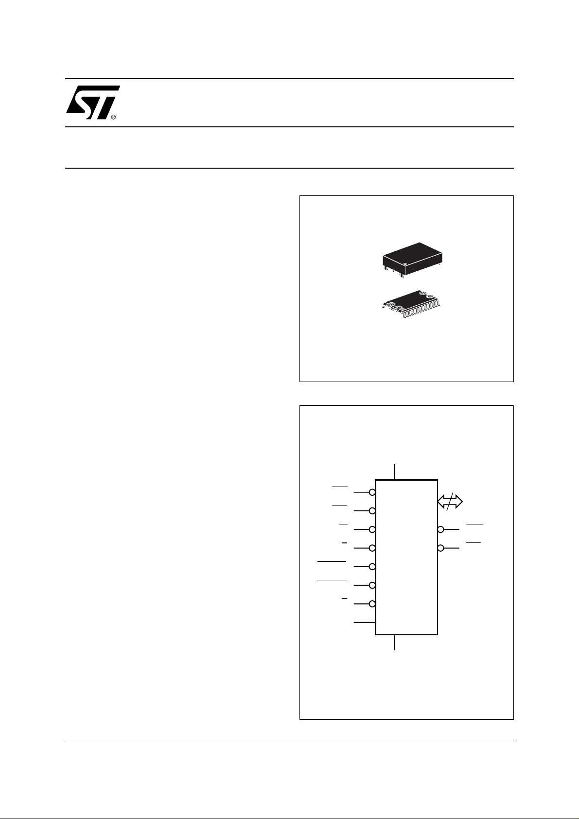
SNAPHAT (SH)
Battery/Crystal
28
1
SOH28 (MH)
Figure 1. Logic Diagram
V
CC
AS0
AS1
W
R
RSTIN1
M48T559Y
8
AD0-AD7
RST
IRQ/FT
DESCRIPTION
The M48T559Y TI MEKEEPER
®
RAM is an 8K x 8
non-volatile static RAM and real time clock. The
monolithic chip is available in the SNAPHAT package to provide a highly integrated battery backedup memory and real time clock solution.
The 28 pin 330mil SOIC provides sockets with
gold plated contacts at both ends for direct connection to a separate SNAPHAT housing cont aining the battery and crystal. The unique design
allows the SNAPHAT battery package to be
mounted on top of the SOIC package after the
completion of the surface mount process.
RSTIN2
WDI
E
V
SS
AI01674B
1/18February 2000
Page 2
M48T559Y
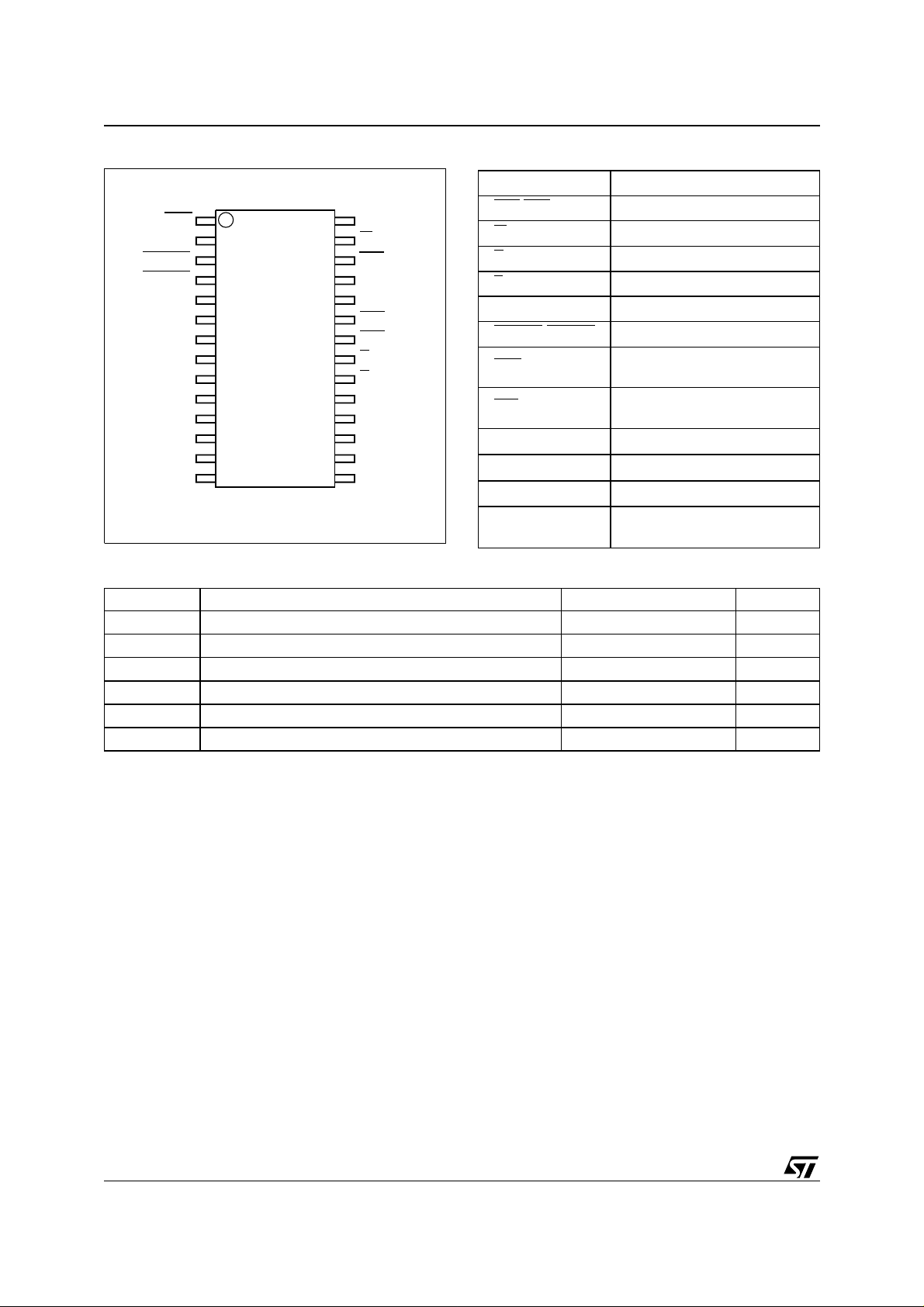
Figure 2. SOIC Connections
RST V
WDI
RSTIN1
RSTIN2
DU
NC
NC
NC
NC
AD0
AD1
V
SS
SS
1
2
3
4
5
6
7
M48T559Y
8
9
10
11
12
13
14
AI01675B
28
27
26
25
24
23
22
21
20
19
18
17
16
15
CC
W
IRQ/FT
DU
DU
AS1
AS0
R
E
AD7
AD6
AD5AD2
AD4
AD3V
Table 1. Signal Names
AD0-AD7 Address/Data
AS0
-AS1 Address Strobes
W
R
E
WDI Watchdog Input
RSTIN1
RST
IRQ
V
V
NC Not Connected Internally
DU
-RSTIN2 Reset Input
/FT
CC
SS
Write Enable
Read Enable
Chip Enable
Power Fail Reset Output
(Open Drain)
Interrupt / Frequency Test
Output (Open Drain)
Supply Voltage
Ground
Don’t Use must be connected
or V
to V
CC
SS
Table 2. Absolute Maximum Ratings
Symbol Parameter Value Unit
T
A
T
STG
V
IO
V
CC
I
O
P
D
Note: Stress es greate r than t hose listed unde r "Absolute Maxi m um Ratings" may c ause perm anent damage to the device. This is a stress
rating onl y and fun ct i onal oper at i on of the device at these or any other conditions above t hose indicated in the operat i onal section of
this specification is not implied. Exposure to the absolute maximum rating conditions for extended periods of time may affect reliability.
CAUTION: Negative undershoo ts bel ow –0.3V are not allowed on any pi n while in the B at tery Back- up mode.
CAUTION: Do NOT wave solder SOIC to avoid damaging SNAPHAT sockets.
Ambient Operating Temperature 0 to 70 °C
Storage Temperature (VCC Off, Oscillator Off)
Input or Output Voltages –0.3 to 7 V
Supply Voltage –0.3 to 7 V
Output Current 20 mA
Power Dissipation 1 W
–40 to 85 °C
Insertion of the SNAPHAT housing after reflow
prevents potential battery and crystal damage due
to the high temperatures required for device surface-mounting. The SNAPHAT housing is keyed
to prevent reverse insertion.
The SOIC and battery/crystal packages are
shipped separately in plastic anti-static tubes or in
Tape & Reel form. For t he 2 8 le ad S OIC , t he ba ttery/crystal package (i.e. SNAPHAT) part number
is "M4T28-BR12SH1".
Caution: Do not place the SNAPHAT battery/crystal top in conductive foam, as this will drain the lithium button-cell battery.
As Figure 3 shows, the static memory array and
the quartz controlled clock oscillator of the
M48T559Y are integrated on one silicon chip. The
2/18
two circuits are interconnected at the up per eight
memory locations to provide user accessible
BYTEWIDE™ clock information in the by tes with
addresses 1FF8h-1FFFh. The clock locations
contain the year, month, date, day, ho ur, minute,
and second in 24 hour BCD format. Corrections for
28, 29 (leap year), 30, and 31 day months are
made automatically. Byte 1FF8h is the clock control register. This byte controls us er ac cess to t he
clock information and also stores the clock calibration setting.
The eight clock bytes are not the actual clock
counters themselves; they are memory locations
consisting of BiPORT™ read/write memory cells.
The M48T559Y includes a clock control circuit
which updates the clock bytes with current infor-
Page 3
Figure 3. Block Diagram
M48T559Y
IRQ/FT
OSCILLATOR AND
CLOCK CHAIN
32,768 Hz
CRYSTAL
POWER
LITHIUM
CELL
VOLTAGE SENSE
AND
SWITCHING
CIRCUITRY
RSTIN1
V
CC
Table 3. Operating Modes
Mode
V
CC
RSTIN2
(1)
Deselect
Write
4.5V to 5.5V
Read
Read
Deselect
Deselect
Note: 1. X = VIH or VIL; VSO = Battery Back-up Swit ch ov er Volta ge.
2. See Table 7 for details.
3. AD0-AD7, AS0
V
to V
SO
PFD
≤ V
SO
, AS1 active when E is high and VCC > V
(min)
(2)
V
PFD
RST
E R W AD0-AD7 Power
V
IH
V
IL
V
IL
V
IL
X X X High Z CMOS Standby
X X X High Z Battery Back-up Mode
PFD
16 x 8 BiPORT
SRAM ARRAY
8176 x 8
SRAM ARRAY
V
SS
E
X X High Z
V
IH
V
IL
V
IH
.
V
IL
V
IH
V
IH
DATA
TRANSCEIVER
UPPER
ADDRESS
LATCH
LOWER
ADDRESS
LATCH
AD0-AD7
Standby
D
D
OUT
IN
Active
Active
High Z Active
W
R
AS1
AS0
AI01676B
(3)
mation once per second. The information can be
accessed by the user i n t he sa me m anner as any
other location in the static memory array.
The M48T559Y also has its own Power-fail Detect
circuit. The control circuitry constantly monitors
the single 5V supply for an out of tolerance condition.
When VCC is out of tolerance, the circuit write protects the SRAM, providing a h igh degree of data
security in the midst of unpredictable system operation brought on by low V
. As VCC falls be low
CC
approximately 3V, the control circuitry connects
the battery which maintains data and clock operation until valid power returns.
3/18
Page 4
M48T559Y
Table 4. AC Measurement Conditions
Input Rise and Fall Times ≤ 5ns
Figure 4. AC Testing Load Circuit
5V
Input Pulse Voltages 0 to 3V
Input and Output Timing Ref. Voltages 1.5V
Note that Output Hi-Z is defined as the point where data is no longer
driven.
Table 5. Capacitance
= 25 °C, f = 1 MHz)
(T
A
(1, 2)
DEVICE
UNDER
TEST
1kΩ
CL includes JIG capacitance
1.9kΩ
OUT
CL = 100pF
Symbol Parameter Test Condition Min Max Unit
V
V
IN
OUT
= 0V
= 0V
10 pF
10 pF
C
IN
C
IO
Note: 1. Effectiv e capacitance measured with power suppl y at 5V .
2. Sampled only, not 100% tested.
3. Outputs deselected.
Input Capacitance
(3)
Input / Output Capacitance
AI01673
Table 6. DC Characteristics
= 0 to 70 °C; VCC = 4.5V to 5.5V)
(T
A
Symbol Parameter Test Condition Min Max Unit
(1)
Input Leakage Current
I
LI
(1)
I
LO
I
LRST
I
I
CC1
I
CC2
V
IL
V
Output Leakage Current
(2)
Input Leakage Current
Supply Current Outputs open 50 mA
CC
Supply Current (Standby) TTL
(3)
Supply Current (Standby) CMOS
(4)
Input Low Voltage –0.3 0.8 V
Input High Voltage 2.2
IH
Output Low Voltage
V
OL
Output Low Voltage (IRQ
(6)
V
OH
Note: 1. Outputs deselected.
Output High Voltage
2. Input leakage current on input RESET p i ns.
3. AD0-AD7, AS0
4. Ne ga t i ve spik e s of –1V allo wed for up t o 10 ns once pe r cycle .
5. The IRQ
6. Measured with Control Bits set as follows: R = '1'; W, ST , FT = '0'.
, AS1 active when E is high and VCC > V
pins is Open Drain.
/FT)
(5)
PFD
0V ≤ V
0V ≤ V
0V ≤ V
E
.
≤ V
IN
CC
≤ V
OUT
≤ V
IN
CC
E
= V
IH
= VCC – 0.2V
I
= 2.1mA
OL
IOL = 10mA
I
= –1mA
OH
CC
±1 µA
±5 µA
100 µA
10 mA
7mA
V
+ 0.3
CC
0.4 V
0.4 V
2.4 V
V
4/18
Page 5
M48T559Y
Table 7. Power Down/Up Trip Points DC Characteristics
(1)
(TA = 0 to 70 °C)
Symbol Parameter Min Typ Max Un it
V
PFD
V
SO
t
DR
Note: 1. All voltages referenced to VSS.
2. At 25°C.
Power-fail Deselect Voltage 4.2 4.35 4.5 V
Battery Back-up Switchover Voltage 3.0 V
(2)
Expected Data Retention Time 7 YEARS
Table 8. Power Down/Up AC Characteristics
(T
= 0 to 70 °C)
A
Symbol Parameter Min Max Unit
t
PD
(1)
t
F
(2)
t
FB
t
R
t
RB
t
REC
Note: 1. V
2. V
PFD
es V
PFD
E at VIH before Power Down
V
(max) to V
PFD
V
(min) to VSS VCC Fall Time
PFD
V
(min) to V
PFD
VSS to V
V
(max) to V
(min).
PFD
(min) to VSS fall time of less than tFB may cause corruption of RAM data.
PFD
(max) to RST High
PFD
(min) fall time of less than tF may result in deselection/write protection not occurring until 200µs after VCC pass-
PFD
(min) VCC Fall Time
PFD
(max) VCC Rise Time
PFD
(min) VCC Rise Time
0 µs
300 µs
10 µs
10 µs
1µs
40 200 ms
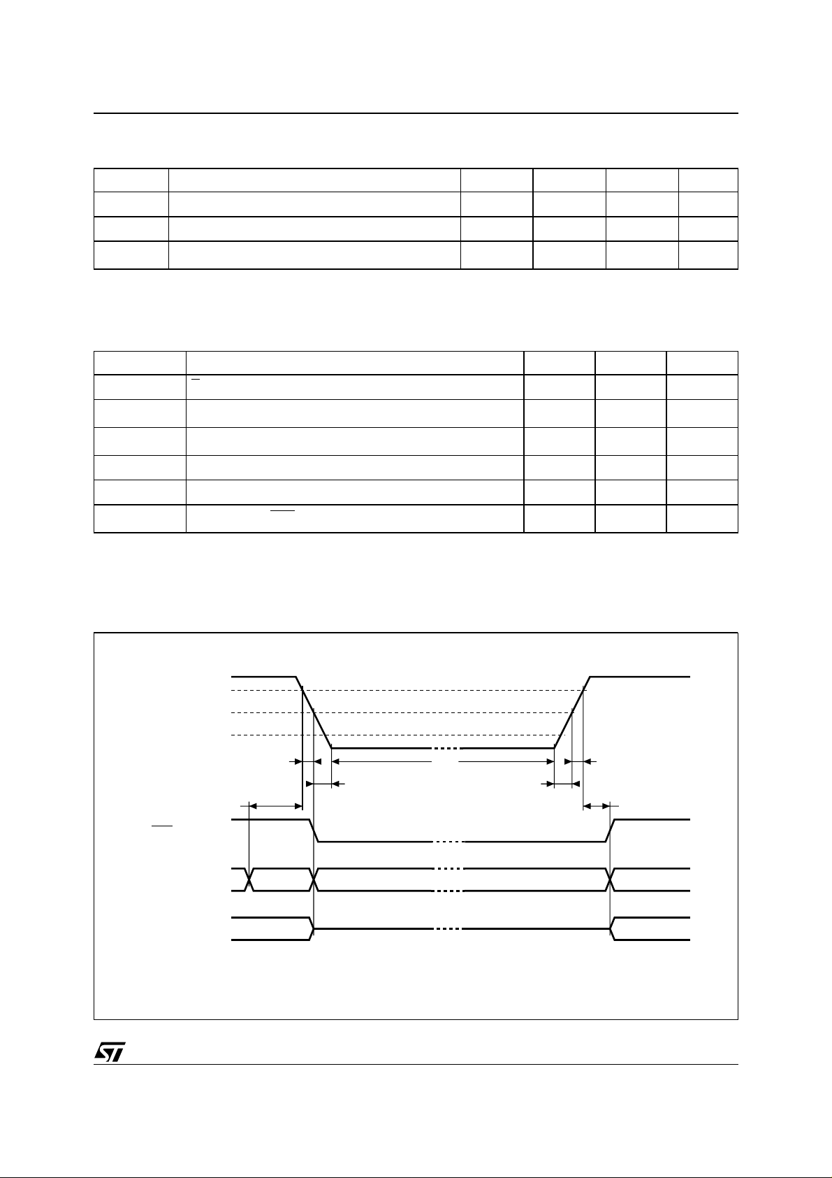
Figure 5. Power Down/Up Mode AC Waveforms
V
CC
V
(max)
PFD
V
(min)
PFD
VSO
tF
tFB
RST
INPUTS
OUTPUTS
VALID VALID
(PER CONTROL INPUT)
tDR
tRB
DON'T CARE
HIGH-Z
tR
tRECtPD
RECOGNIZEDRECOGNIZED
(PER CONTROL INPUT)
AI01384D
5/18
Page 6
M48T559Y
Table 9. AC Characteristics
(T
= 0 to 70 °C; VCC = 4.5V to 5.5V)
A
Symbol Parameter
t
AS
t
AH
t
DS
t
DH
t
RLDV
t
RLRH
t
RHDZ
t
WLWH
t
ELEH
t
ASLASH
t
ASHRL
t
ASHWL
t
ELRL
t
EHDZ
t
ELWL
Address Setup Time 20 ns
Address Hold Time 0 ns
Data Setup Time 60 ns
Data Hold Time 0 ns
Read Enable Access Time 70 ns
R Pulse Width Low 70 ns
Read Enable High to Output High Z 25 ns
W Pulse Width Low 50 ns
E Pulse Width Low 50 ns
AS0, AS1 Pulse Width Low 15 ns
AS0, AS1 High to R Low 15 ns
AS0, AS1 High to W Low 15 ns
Chip Enable Low to Read Enable Low 0 ns
Chip Enable High to Data Output Hi-Z 0 ns
Chip Enable Low to Write Enable Low 0 ns
M48T559Y
Unit
Min Max
RAM OPERATION
Four control signals, AS0
, AS1, R and W, ar e us ed
to access the M48T559Y. The address latches are
loaded from the address/data b us in respon se to
rising edge signals applied to the Address Strobe
0 (AS0
) and Address Strobe 1 (AS1) signals. AS0
is used to latch the lower 8 b its of address, and
AS1
is used to latch the upper 5 bits of address.
It is not however necessary to follow any particular
order. The inputs are in parallel for the two address bytes (upper and lower) and can be latched
in any order as long as the correct strobe is used.
It is necessary to meet the set-up and hold times
given in the AC specifications with valid address
information in order to properly latch the address.
If the upper and/or lower order addresses are correct from a prior cycle, it is not necessary to repeat
the address latching sequence.
A write operation requires valid dat a to be placed
on the bus (AD0-AD7), followed by the activation
of the Write Enabl e (W
) line. Data on t he bus wi ll
be written to the RAM, provided that the write timing specific ations are met. During a read cycl e, the
Read Enable (R
) signal is driven active. Data from
the RAM will become valid on the bus provided
that the RAM read access timing specifications are
met.
The W
and R signals should never be active at the
same time. In addition, E
must be active before
any control line is recognized (except for AD0-AD7
and AS0
, AS1).
RESET INPUT
The M48T559Y provides two debounced inputs
which can generate an output Reset. The duration
and function of the Reset output is identical to a
Reset generated by a power cycle. Pulses shorter
than t
and tR2 will not generate a Reset condi-
R1
tion (see Table 12 and Figure 13).
DATA RETENTION MODE
Should the supply voltage decay, the RAM will automatically power-fail deselect, write protecting itself w hen V
falls within the V
CC
PFD
(max), V
PFD
(min) window. All outputs become high impedance, and all inputs are treated as "don't care."
Note: A power failure during a write cycle may corrupt data at the currently addressed location, but
does not jeopardize the rest of the RAM's content.
At voltages below V
(min), the user can be as-
PFD
sured the memory will be in a write protected state,
provided the V
fall time is no t les s than tF.
CC
6/18
Page 7

Figure 6. Read Mode AC Waveforms
E
M48T559Y
tELEH
tASLASH
AS0
AS1
R
tAS tAH
AD0-AD7
LOW ADDRESS VALID
Note: AD5-AD 7 are don’t care when latchi ng upper address.
Figure 7. Write Mode AC Waveform
tASLASH
tAS tAH
UPPER ADDRESS VALID
tRLDV
tELRL
tRLRHtASHRL
DATA OUT
VALID
tEHDZ
tRHDZ
AI01671B
E
tASLASH
AS0
AS1
W
tAS tAH
AD0-AD7
LOW ADDRESS VALID
Note: AD5-AD 7 are don’t care when latchi ng upper address.
tASLASH
tAS tAH
UPPER ADDRESS VALID
tELEH
tELWL
tDS
DATA IN VALID
tEHDZ
tWLWHtASHWL
tDH
AI01672B
7/18
Page 8

M48T559Y
Table 10. Register Map
Address
Data
D7 D6 D5 D4 D3 D2 D1 D0
1FFFh 10 Years Year Year 00-99
1FFEh 0 0 0 10 M Month Month 01-12
1FFDh 0 0 10 Date Date Date 01-31
1FFCh 0 FT 0 0 0 Day Day 01-07
1FFBh 0 0 10 Hours Hours Hour 00-23
1FFAh 0 10 Minutes Minutes Minutes 00-59
1FF9h ST 10 Seconds Seconds Seconds 00 -59
1FF8h W R S Calibration Control
1FF7h WDS BMB4 BMB3 BMB2 BMB1 BMB0 RB1 RB0 Watchdog
1FF6hAFEYABEYYYYYInterrupts
1FF5h RPT4 Y Al. 10 Date Alarm Date Alarm Date 01-31
1FF4h RPT3 Y Al. 10 Hours Alarm Hours Alarm Hours 00-23
1FF3h RPT2 Alarm 10 Minutes Alarm Minutes Alarm Minutes 00-59
Function/Rang e
BCD Format
1FF2h RPT1 Alarm 10 Seconds Alar m Seco nds Alarm Secon ds 00-59
1FF1hYYYYYYYY Unused
1FF0hWDFAFZBLZZZZ Flags
Keys: S = SIGN Bit
FT = FREQUENCY TEST Bit
R = READ Bit
W = WRITE Bit
ST = STOP Bit
0 = Must be set to zero
Y = ’1’ or ’0’
Z = ’0’ and ar e Read only
AF = Alarm Flag
The M48T559Y may respond to transient noise
spikes on V
during the time the device is sampling V
that reach into the deselect window
CC
. There-
CC
fore, decoupling of the power supply lines is rec-
BL = Battery Low
WDS = Watch dog Steering Bit
BMB0-BMB4 = Watchdog M ultiplier Bits
RB0-RB1 = Wat chdog R e s o l ution Bits
AFE = Alarm Flag Enable
ABE = Alarm in Battery Back-up Mode Enable
RPT1- R PT4 = Alarm Repeat Mode Bits
WDF = Watchdog Flag
nal V
reaches V
. Write protection continues until V
CC
(max) plus t
PFD
. For more i nforma-
REC
tion on Battery Storage Life refer to the Application
Note AN1012.
ommended.
When V
drops below VSO, the control circuit
CC
switches power to the internal battery which preserves data and powers the clock. The internal
button cell will maintain da ta in t he M 48T559Y for
an accumulated period of at least 7 years when
is less than VSO. As system power returns
V
CC
and V
rises above VSO, the battery is discon-
CC
nected, and the power supply is switched to exter-
POWER-ON RESET
The M48T559Y continuously monitors V
V
falls to the power fail detect trip point, the RST
CC
pulls low (open drain) and remains low on powerup for 40ms to 200m s after V
external pull-up resistor to V
passes V
CC
is required (1kΩ re-
CC
sistor is recommended). The reset pulse remains
active with V
at VSS.
CC
. When
CC
PFD
CC
. An
8/18
Page 9

M48T559Y
CLOCK OPERATIONS
Reading the Clock
Updates to the TIMEKEEPER registers should be
halted before clock data is read to prevent reading
data in transition. Because the BiPORT TIMEKEEPER cel ls in th e RAM array a r e on ly data r e gisters, and not the actual clock counters, updating
the registers can be halted without disturbing the
clock itself.
Updating is halted when a '1' is written to the
READ bit, D6 in the Control register (1FF8h). As
long as a '1' remains in that position , updating is
halted.
After a halt is issued, the registers reflect the
count; that is, the day, date, and the time that were
current at the moment the halt command was issued.
All of the TIMEKEEPER registers are updated simultaneously. A halt will not interrupt an update in
progress. Updating is within a second after the bit
is reset to a '0'.
Setting the Clock
Bit D7 of the Control register (1FF8h) is the
WRITE bit. Setting the WR ITE bit to a '1', like the
READ bit, halts update s to the TIMEKEEPER registers. The user can then loa d them with the correct day, date, and time data in 24 hour BCD
format (see Table 9). Resetting the WRITE bit t o a
'0' then transfers the values of all time registers
(1FF9h-1FFFh) to the actual TIMEKEEPER
counters and allows normal operation to re sume.
After the WRITE bit is reset, the next clock update
will occur in one second.
See the Application Note AN923 "TIMEKEEPER
rolling into the 21st century" for information on
Century Rollover.
Stopping and Starting the Oscillator
The oscillator may be stopped at any time. If the
device is going to spend a significant amount of
time on the shelf, the oscillator can be turned off to
minimize current drain on the battery. The STOP
bit is the MSB of the seconds register. Setting it to
a ’1’ stops the oscillator. The M48T559Y is
shipped from STMicroelectronics with the STOP
bit set to a ’1’. When reset to a ’0’, the M48T559Y
oscillator starts within one second.
Calib ratin g t h e C lock
The M48T559Y is driven by a quartz controlled oscillator with a nominal frequency of 32,768Hz. The
devices are tested not to exceed 35 ppm (parts per
million) oscillator frequency error at 25° C, which
equates to about ±1.53 m inutes per month. With
the calibration bits properly set, the accuracy of
each M48T559Y improves to b etter than ±4 ppm
at 25°C.
The oscillation rate of any crystal changes with
temperature (see Figure 10). Most clock chips
compensate for crystal frequency and temperature shift error with cumbersome trim capacitors.
The M48T559Y design, however, employs periodic counter correction. The calibration circuit adds
or subtracts counts from the oscillator divider circuit at the divide by 256 stage, as shown in Figure
9. The number of times pulses are bl anked (subtracted, negative calibration) or split (ad ded, pos itive calibration) depends upon the value loaded
into the five bit Calibration byte found in the Control Register. Adding count s speeds the clock up,
subtracting counts slows the clock down.
Figure 8. Clock Calibration
NORMAL
POSITIVE
CALIBRATION
NEGATIVE
CALIBRATION
AI00594B
9/18
Page 10

M48T559Y
Figure 9. Crystal Accuracy Across Temperature
ppm
20
0
-20
-40
∆F
= -0.038 (T - T
-60
-80
-100
0 5 10 15 20 25 30 35 40 45 50 55 60 65 70
F
ppm
2
C
T0 = 25 °C
The Calibration byte occupies the five lower order
bits (D4-D0) in the Control r egister (1FF8h). These
bits can be set to represent any value between 0
and 31 in binary form. Bit D5 is a Sign bit; ’1’ indicates positive calibration, ’0’ indicates negative
calibration. Calibration occurs within a 64 m inute
cycle. The first 62 m inutes i n t he c ycle m ay , onc e
per minute, have one second either shortened by
128 or lengthened by 256 oscillator cycles.
If a binary ’1’ is loaded into the register, only the
first 2 minutes in the 64 minute cycle will be modified; if a binary 6 is loaded, the first 12 will be affected, and so on.
Therefore, each cal ibration step has the effect of
adding 512 or subtracting 256 oscillator cycles for
every 125,829,120 actual oscillator cycles, that is,
+4.068 or -2.034 ppm of adjustment per calibration
step in the calibration register. Assuming that the
oscillator is in fact running at exactly 32,768Hz,
each of the 31 in crements in the Calibration by te
would represent +10.7 or -5.35 seconds per month
which corresponds to a total range of +5.5 or - 2.75
minutes per month.
Two methods are available for ascertaining how
much calibration a given M48T559 Y may require.
)2 ± 10%
0
°C
AI02124
The first involves simply setting the clock, letting it
run for a month and comparing it to a known accurate reference (like WWV broadcasts). While that
may seem crude, it allows the designer to give the
end user the ability to calibrate his clock as his environment may require, even after the final product
is packaged in a non-user serviceable enclosure.
All the designer has to do is provide a simple utility
that accesses the Calibration byte.
The second approach is better suit ed to a manufacturing environment, and involves the use of the
/FT pin. The pin will toggle at 512Hz when the
IRQ
Stop bit (D7 of 1FF9h) is ’0’, the FT bit (D6 of
1FFCh) is ’1’, the AFE bit (D7 of 1FF6h) is ’0’, and
the Watchdog Steering bit (D7 of 1FF7h) is ’1’ or
the Watchdog Register is reset (1FF7h = 0).
Any deviation from 512Hz indicates the degree
and direction of oscillator frequency shift at the test
temperature. For example, a reading of 512.01024
Hz would indicate a +20 ppm oscillator frequency
error, requiring a -10 (WR001010) to be loaded
into the Calibration Byte for correction. Not e that
setting or changing the Calibration Byte does not
affect the Frequency test output frequency.
The FT bit is cleared on power-down.
10/18
Page 11

M48T559Y
For more information on calibration, see the Application Note AN934 "TIMEKEEPER Calibration".
The IRQ
/FT pin is an open drain out put which requires a pull-up resistor for proper operation. A
500-10kΩ resistor is recommended in order to
control the rise time.
SETTING ALARM CLOCK
Registers 1FF5h-1FF2h contain the alarm settings. The alarm can be configured to go off at a
prescribed time on a specific day of the month or
repeat every day, hour, minute, or sec ond. It can
also be programmed to go off while the M48T559Y
is in the battery back-up mode of operation to
serve as a system wake-up call.
RPT1-RPT4 put the alarm in the repeat mode of
operation. Table 11 shows the possible configurations. Codes not listed in the table default to the
once per second mode t o qu ick ly alert t he user of
an incorrect alarm setting.
Note: User must transition address (or toggle chip
enable) to see Flag bit change.
When the clock information matches the alarm
clock settings based on the m atch criteria d efined
by RPT1-RPT4, AF (Alarm Flag) is set. If AFE
(Alarm Flag Enable) is also set, the alarm condition activa tes the IRQ
/FT pin. To disable alarm,
write ’0’ to the Alarm Date registers and RPT1-4.
The alarm flag and the I RQ
/FT output are cleared
by a read to the Flags register as shown in Figure
11.
Note: If an alarm cond ition occurs while t he flags
register address is latched into the address buffer,
the alarm flag will not be set until an address other
than the flags register (1FF0h) is latched into the
address buffer. This will insure that the alarm flag
will not be inadvertently reset while reading the
flag register. To properly check to see if an alarm
condition has occurred while readin g the f lag register, the user is requ ired to latch, read or write to
an alternate address and then re-read t he alarm
flag.
The IRQ
tery back-up mode. The IRQ
/FT pin can also be activated in the bat-
/FT will go low if an
alarm occurs and both ABE (Alarm in Battery
Back-up Mode Enable) and AFE are set. The ABE
and AFE bits are reset during power-up, therefore
an alarm generated during power-up will only set
AF. The user can read the Flag Register at syst em
boot-up to determine if an alarm was generated
while the M48T559Y was in the deselect mode
during power-up. Figure 12 illustrates the back-up
mode alarm timing.
Table 11. Alarm Repeat Mode
RPT4 RPT3 RPT2 RPT1 Alarm Activated
1 1 1 1 Once per Second
1 1 1 0 Once per Minute
1 1 0 0 Once per Hour
1 0 0 0 Once per Day
Figure 10. Interrupt Reset Waveforms
AD0-AD7
R
ACTIVE FLAG BIT
IRQ/FT
0 0 0 0 Once per Month
ADDRESS 1FF0h
AI01677B
11/18
Page 12

M48T559Y
Figure 11. Back-up Mode Alarm Waveforms
V
CC
V
(max)
PFD
V
(min)
PFD
V
SO
AFE bit in Interrupt Register
AF bit in Flags Register
IRQ/FT
tREC
HIGH-Z
WATCHD OG TI M E R
The watchdog timer can be used to detect an outof-control microprocessor. The user programs the
watchdog timer by setting the desired amount of
time-out into the eight bit Watchdog Reg ister (Address 1FF7h). The five bits (BMB4-BMB0) store a
binary multiplier and the two lower order bits (RB1RB0) select the resol ution, where 00 = 1/16 sec ond, 01 = 1/4 second, 10 = 1 second, an d 11 = 4
seconds. The amount of time-out is then determined to be the mult iplication of the f ive bit multiplier value with the resolution. (For example:
writing 00001110 in the Watchdog Register = 3 x
1 or 3 seconds).
Note: Accuracy of timer is within ± the selected
resolution.
If the processor does not reset the timer within the
specified period, the M48T559Y sets the WDF
(Watchdog Flag) and generates a watchdog interrupt or a microprocessor reset. WDF is reset by
reading the Flags Register (Address 1FF0h).
The most significant bit of the Watchdog Register
is the Watchdog Steering Bit. When set to a '0', the
watchdog will activate the IRQ
/FT pin when timedout. When WDS is set to a '1', the watchdog will
output a negative pulse on the RST
pin for a duration of 40ms to 200ms. The Watchdog register will
reset to a '0' at the end of a watchdog time-out
when the WDS bit is set to a '1'.
HIGH-Z
AI01678C
The watchdog timer can be reset by two methods:
– a transition (high-to-low or low-to-high) can be
applied to the Watchdog input pin (WDI)
or
– the microprocessor can perform a write of the
Watchdog Register. The time-out period then
starts over The WDI pin contains a pull-up resis-
tor and therefore can be left unconnected if not
used.
The watchdog timer will be reset on each transition
(edge) seen by the WDI pin. In order t o pe rform a
software reset of the Watchdog timer, the original
time-out period can be written into the Watchdog
Register, effectively restarting the count-down cycle.
Should the watchdog timer time-out, and the WDS
bit is programmed to output an interrupt, a value of
00h needs to be written to the Watchdog Register
in order to clear the IRQ
/FT pin. This will also disable the watchdog function until it is again programmed correctly. A rea d of the Flags Register
will reset th e Watchdog Fl ag (D7; R egister MSB-
15).
The watchdog function is automatically disabled
upon power-down and the Watchd og Register is
cleared. If the watchdog function is set to output to
the IR Q
/FT pin and the frequency tes t function is
activated, the watchdog or alarm function prevails
and the frequency test function is denied.
12/18
Page 13

Figure 12. Reset Timing Waveforms
RSTIN1
RSTIN2
RST
tR2
Hi-Z
M48T559Y
Hi-Z
tR1 tR1HRZ
Table 12. Reset AC Characteristics (T
Symbol Parameter Min Max Unit
t
R1
t
R2
t
R1HRZ
t
R2HRZ
RSTIN1 Low to RST Low 50 200 ns
RSTIN2 Low to RST Low 20 100 ms
RSTIN1 High to RST Hi-Z 40 200 ms
RSTIN2 High to RST Hi-Z 40 200 ms
BATTERY LOW WARNING
The M48T559Y checks its battery voltage on power-up. The BL (Battery Low) bit (D4 of 1FF 0h) wi ll
be set on power-up if the battery voltage is less
than 2.5V (typical).
POWER-ON DEFAULTS
Upon application of power to the de vice, the following register bits are set to a ’0’ state: WDS;
BMB0-BMB4 ; RB0 - R B1 ; AFE; ABE; W; R; FT.
= 0 to 70°C; VCC = 4.5V to 5.5V)
A
ative voltage spikes on V
below V
by as much as one Volt. These nega-
SS
tive spikes can cause data corruption in the SRAM
while in battery backup mode. To protect from
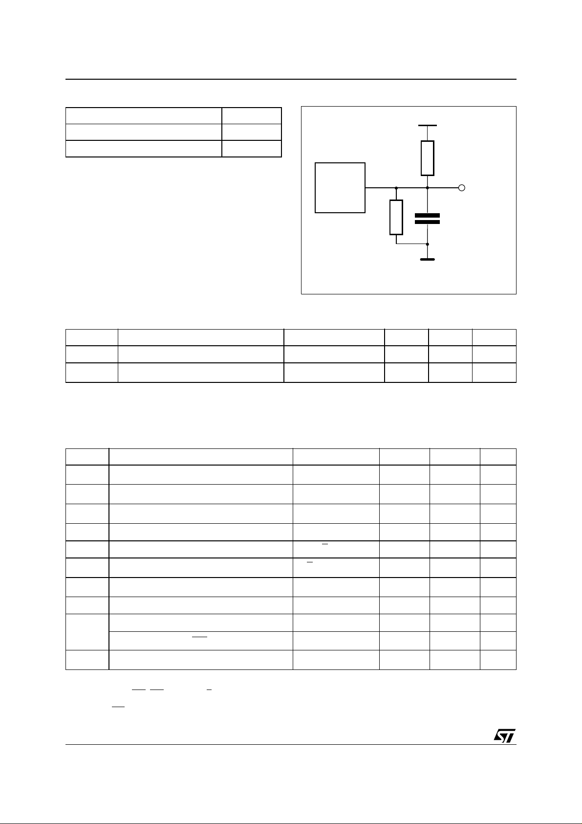
these voltage spikes, it is recommended to connect a schottky diode from V
connected to V
CC
1N5817 is recommended for through hole and
MBRS120T3 is recommended for surface mount.
Figure 13. Supply Voltage Protection
, anode to VSS). Schottky diode
tR2HRZ
AI01679
that drive it to values
CC
to VSS (cathode
CC
POWER SUPPLY DECOUPLING
and UNDERSHOOT PROTECTION
transients, including those produced by output
I
CC
switching, can produce voltage fluctuations, resulting in spikes on the V
bus. These transients
CC
V
CC
V
CC
can be reduced if capacitors are used to store energy, which stabilizes the V
stored in the bypass capacitors will be released as
bus. The energy
CC
0.1µF DEVICE
low going spikes are generated or energy will be
absorbed when overshoots occur. A ceramic by-
pass capacitor value of 0.1µF (as shown in Figure
V
SS
14) is recommended in order to provide the needed filtering.
In addition to transients that are caused by normal
SRAM operation, power cycling can generate neg-
AI02169
13/18
Page 14

M48T559Y
Table 13. Ordering Information Scheme
Example: M48T559Y MH 1 TR
Device Type
M48T
Supply Voltage and Write Protect Voltage
559Y = V
Package
(1)
MH
Temperature Range
1 = 0 to 70 °C
Shipping Method for SOIC
blank = Tubes
TR = Tape & Reel
= 4.5V to 5.5V; V
CC
= SOH28
= 4.2V to 4.5V
PFD
Note: 1. The SOIC package (SOH28) requires the battery/crystal package (SNAPHAT) which is ordered separately under the part number
"M48T28-BR12SH1" in plastic tube or "M4T28-BR12SH1TR" in Tape & Reel form.
Caution: Do not place the SNAPHAT battery/crystal pac kage "M4T28-BR12SH1" in c onductive foam since will drai n the lithium butt on-cell
battery.
For a list of available options (Speed, Pac kage, etc...) or for furthe r information on any aspect of this device, please contact the ST Sales Office nearest to you.
Table 14. Revision History
Date Revision Details
June 1998 F irst Issue
Description Paragraph changed
Setting Alarm Clock paragraph changed
02/07/00
M4T28-BR12SH SNAPHAT Housing for 48mAh Battery & Crystal Package added (Table 16)
Power Down/Up Mode AC Waveforms changed (Figure 5)
Back-up Mode Alarm Waveforms changed (Figure 11)
14/18
Page 15

M48T559Y
Table 15. SOH28 - 28 lead Plastic Small Outline, 4-socket battery SNAPHAT, Package Mechanical Data
Symb
Typ Min Max Typ Min Max
A 3.05 0.120
A1 0.05 0.36 0.002 0.014
A2 2.34 2.69 0.092 0.106
B 0.36 0.51 0.014 0.020
C 0.15 0.32 0.006 0.012
D 17.71 18.49 0.697 0.728
E 8.23 8.89 0.324 0.350
e 1.27 – – 0.050 – –
eB 3.20 3.61 0.126 0.142
H 11.51 12.70 0.453 0.500
L 0.41 1.27 0.016 0.050
α 0° 8° 0° 8°
N 28 28
mm inches
CP 0.10 0.004
Figure 14. SOH28 - 28 lead Plastic Small Outline, 4-socket battery SNAPHAT, Package Outline
A2
A
C
Be
eB
CP
D
N
E
H
LA1 α
1
SOH-A
Drawing is not to scale.
15/18
Page 16

M48T559Y
Tab l e 16 . M4T28- BR12SH SNAPHAT Ho u sing for 4 8mAh Batter y & Cr ystal, Pack ag e Mechanic al Data
Symb
Typ Min Max Typ Min Max
A 9.78 0.385
A1 6.73 7.24 0.265 0.285
A2 6.48 6.99 0.255 0.275
A3 0.38 0.015
B 0.46 0.56 0.018 0.022
D 21.21 21.84 0.835 0.860
E 14.22 14.99 0.560 0.590
eA 15.55 15.95 0.612 0.628
eB 3.20 3.61 0.126 0.142
L 2.03 2.29 0.080 0.090
mm inches
Figure 15. M4T28-BR12SH SNAPHAT Housing for 48mAh Battery & Crystal, Package Outline
A2
A3
L
eA
D
A1
A
B
eB
E
SHTK-A
Drawing is not to scale.
16/18
Page 17

M48T559Y
Table 17. M4T28-BR12SH SNAPHAT Housing for 120mAh Battery & Crystal, Package Mechanical Data
Symb
Typ Min Max Typ Min Max
A 10.54 0.415
A1 8.00 8.51 0.315 0.335
A2 7.24 8.00 0.285 0.315
A3 0.38 0.015
B 0.46 0.56 0.018 0.022
D 21.21 21.84 0.835 0.860
E 17.27 18.03 0.680 0.710
eA 15.55 15.95 0.612 0.628
eB 3.20 3.61 0.126 0.142
L 2.03 2.29 0.080 0.090
mm inches
Figure 16. M4T28-BR12SH SNAPHAT Housing for 120mAh Battery & Crystal, Package Outline
A2
A3
L
eA
D
A1
A
B
eB
E
SHTK-A
Drawing is not to scale.
17/18
Page 18

M48T559Y
.
Information furnished is believed to be ac curate and reliable. However, STMicroelectro ni cs assumes no resp onsibility for the cons equences
of use of such information nor for any infringement of patents or other rights of third parties which may result from its use. No license is granted
by implic ation or otherwise under any patent or pat ent rights of STMicroelectronics. Specifications mentioned in thi s publicati on are s ubject
to change without notice. This publication supersedes and replaces all information previously supplied. STMicroelectronics products are not
authorized for use as cri tical comp onents in life support devi ces or systems without express written approv al of STMicroel ectronics.
The ST log o i s registered trademark of STMicroelectronics
1998 STMicroel e ctronics - All Rights Reserved
All other names are the property of their respective ow ners.
Australi a - Brazil - Chi na - Finland - F rance - Germ any - Hong K ong - India - It al y - Japan - Ma la ys i a - Malta - Morocco -
Singapor e - Spain - Sweden - Switzerl and - United Kingdom - U .S .A.
STMicroelect ro n ics GRO UP OF COMPANI ES
http://www.st.com
18/18
 Loading...