

Page 1
DEVICES INCORPORATED
LSH33
32-bit Barrel Shifter with Registers
LSH33
DEVICES INCORPORATED
32-bit Barrel Shifter with Registers
FEATURES DESCRIPTION
❑❑
❑ 32-bit Input, 32-bit Output Multi-
❑❑
plexed to 16 Lines
❑❑
❑ Full 0-31 Position Barrel Shift
❑❑
Capability
❑❑
❑ Integral Priority Encoder for 32-bit
❑❑
Floating Point Normalization
❑❑
❑ Sign-Magnitude or Two’s Comple-
❑❑
ment Mantissa Representation
❑❑
❑ 32-bit Linear Shifts with Sign or
❑❑
Zero Fill
❑❑
❑ Independent Priority Encoder
❑❑
Outputs for Block Floating Point
❑❑
❑ 68-pin PLCC, J-Lead
❑❑
The LSH33 is a 32-bit high speed
shifter designed for use in floating
point normalization, word pack/
unpack, field extraction, and similar
applications. It has 32 data inputs,
and 16 output lines. Any shift configuration of the 32 inputs, including
circular (barrel) shifting, left shifts
with zero fill, and right shifts with
sign extension are possible. In addition, a built-in priority encoder is
provided to aid floating point normalization.
Input/Output registers provide
complete pipelined operation. Both
have independent bypass paths for
complete flexibility. When FTI = 1,
the input registers are bypassed.
Likewise, when FTO= 1, the output
registers are bypassed.
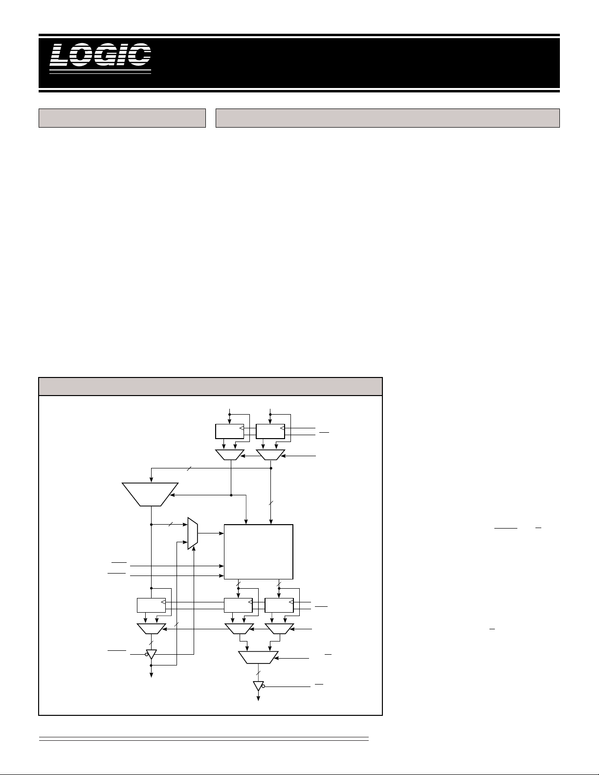
LSH33 BLOCK DIAGRAM
I31-I
0
32
32-bit
SHIFT
ARRAY
GG
2:1
16
RIGHT/LEFT
FILL/WRAP
NORM
32:5
PRIORITY
ENCODE
2:1
5
SI/O4-SI/O
SIGN
GG
32
5
2:1
G
5
0
2:1 2:1
BARREL
16
2:1 2:1
SHIFT ARRAY
The 32 inputs, which can be registered, to the LSH33 are applied to a
32-bit shift array. The 32 outputs,
which can also be registered, of this
array are then multiplexed down to
16 lines for presentation at the device
outputs. The array may be configured
such that any contiguous 16-bit field
(including wraparound of the 32
inputs) may be presented to the
output pins under control of the shift
code field (wrap mode). Alternatively, the wrap feature may be
disabled, resulting in zero or sign bit
fill, as appropriate (fill mode). The
shift code control assignments and the
resulting input to output mapping for
the wrap mode are shown in Table 1.
Essentially the LSH33 is configured as
a left shift device. That is, a shift code
of 000002 results in no shift of the
input field. A code of 000012 provides
an effective left shift of 1 position, etc.
CLK
ENI
When viewed as a right shift, the shift
code corresponds to the two’s complement of the shift distance, i.e., a shift
FTI
code of 111112 (–110) results in a right
shift of one position, etc.
When not in the wrap mode, the
LSH33 fills bit positions for which
there is no corresponding input bit.
The fill value and the positions filled
depend on the RIGHT/LEFT (R/L)
direction pin. This pin is a don’t care
input when in wrap mode. For left
shifts in fill mode, lower bits are filled
16
CLK
ENO
FTO
with zero as shown in Table 2. For
right shifts, however, the SIGN input
is used as the fill value. Table 3
depicts the bits to be filled as a
function of shift code for the right shift
case. Note that the R/L input changes
only the fill convention, and does not
MS/LS
OE
affect the definition of the shift code.
Y15-Y
0
Special Arithmetic Functions
1
08/16/2000–LDS.33-O
Page 2
DEVICES INCORPORATED
LSH33
32-bit Barrel Shifter with Registers
TABLE 1. WRAP MODE SHIFT CODE DEFINITIONS
Shift CodeShift Code
Shift Code
Shift CodeShift Code
00000 I31 I30 I29 • • • I16 I 15 • • • I2 I1 I0
00001 I30 I29 I28 • • • I15 I 14 • • • I1 I0 I31
00010 I29 I28 I27 • • • I14 I 13 • • • I0 I31 I 30
00011 I28 I27 I26 • • • I13 I 12 • • • I31 I 30 I 29
• •••• • •• •• • ••••
• •••• • •• •• • ••••
• •••• • •• •• • ••••
01111 I16 I15 I14 • • • I1 I0• • •I19 I18 I17
10000 I15 I14 I13 • • • I0 I31 • • • I18 I 17 I16
10001 I14 I13 I12 • • • I31 I 30 • • • I17 I16 I15
10010 I13 I12 I11 • • • I30 I 29 • • • I16 I15 I14
• •••• • •• •• • ••••
• •••• • •• •• • ••••
• •••• • •• •• • ••••
11100 I3 I2 I1• • •I20 I 19 • • • I6 I5 I 4
11101 I2 I1 I0• • •I19 I 18 • • • I5 I4 I 3
11110 I1 I0 I31 • • • I18 I 17 • • • I4 I3 I2
11111 I0 I31 I30 • • • I17 I 16 • • • I3 I2 I1
YY
YY
3131
Y
31
3131
YY
YY
3030
30
3030
2929
Y
29
2929
YY
Y
YY
• • •• • •
• • •
• • •• • •
YY
YY
1616
16
1616
1515
Y
15 • • •
1515
YY
Y
YY
YY
YY
22
Y
2
22
YY
YY
11
Y
YY
00
1
Y
0
11
00
YY
In fill mode, as in wrap mode, the shift
code input represents the number of
shift positions directly for left shifts,
but the two’s complement of the shift
code results in the equivalent right
shift. However, for fill mode the R/L
input can be viewed as the most
significant bit of a 6-bit two’s complement shift code, comprised of R/L
concatenated with the SI4–SI0 lines.
Thus, a positive shift code (R/L = 0)
results in a left shift of 0–31 positions,
and a negative code (R/L = 1) a right
shift of up to 32 positions. The LSH33
can thus effectively select any contiguous 32-bit field out of a (sign extended
and zero filled) 96-bit "input."
OUTPUT MULTIPLEXER
The shift array outputs can be registered and then applied to a 2:1 multiplexer controlled by the MS/LS select
line. This multiplexer makes available
at the output pins either the most
significant or least significant 16
outputs of the shift array.
TABLE 2. FILL MODE SHIFT CODE DEFINITIONS — LEFT SHIFT
Shift CodeShift Code
Shift Code
Shift CodeShift Code
00000 I31 I30 I29 • • • I16 I 15 • • • I2 I1 I0
00001 I30 I29 I28 • • • I15 I 14 • • • I1 I0 0
00010 I29 I28 I27 • • • I14 I 13 • • • I0 00
00011 I28 I27 I26 • • • I13 I 12 • • • 000
• •••• • •• •• • ••••
• •••• • •• •• • ••••
• •••• • •• •• • ••••
01111 I16 I15 I14 • • • I1 I0• • •000
10000 I15 I14 I13 • • • I0 0 • • • 000
10001 I14 I13 I12 • • • 00• • • 000
10010 I13 I12 I11 • • • 00• • • 000
• •••• • •• •• • ••••
• •••• • •• •• • ••••
• •••• • •• •• • ••••
11100 I3 I2 I1• • • 00• • • 000
11101 I2 I1 I0• • • 00• • • 000
11110 I1 I0 0 • • • 00• • • 000
11111 I0 00• • • 00• • • 000
YY
YY
3131
Y
31
3131
YY
YY
3030
30
3030
2929
Y
29
2929
YY
Y
YY
• • •• • •
• • •
• • •• • •
YY
YY
1616
16
1616
1515
Y
15 • • •
1515
YY
Y
YY
YY
YY
22
Y
2
22
YY
YY
11
Y
YY
00
1
Y
0
11
00
YY
PRIORITY ENCODER
The 32-bit input bus drives a priority
encoder which is used to determine
the first significant position for
purposes of normalization. The
priority encoder produces a five-bit
code representing the location of the
first non-zero bit in the input word.
Code assignment is such that the
priority encoder output represents the
number of shift positions required to
left align the first non-zero bit of the
input word. Prior to the priority
encoder, the input bits are individually exclusive OR’ed with the SIGN
input. This allows normalization in
floating point systems using two’s
complement mantissa representation.
A negative value in two’s complement
representation will cause the exclusive
OR gates to invert the input data to
the encoder. As a result, the leading
significant digit will always be "1."
Special Arithmetic Functions
2
08/16/2000–LDS.33-O
Page 3
DEVICES INCORPORATED
LSH33
32-bit Barrel Shifter with Registers
TABLE 3. FILL MODE SHIFT CODE DEFINITIONS — RIGHT SHIFT
Shift CodeShift Code
Shift Code
Shift CodeShift Code
00000 S S S • • • SS• • •SSS
00001 S S S • • • SS• • •SSI31
00010 S S S • • • SS• • •SI31 I30
00011 S S S • • • SS• • •I31 I30 I 29
• •••• • •• •• • ••••
• •••• • •• •• • ••••
• •••• • •• •• • ••••
01111 S S S • • • SS• • •I19 I18 I 17
10000 S S S • • • SI31 • • • I18 I17 I16
10001 S S S • • • I31 I 30 • • • I17 I16 I15
10010 S S S • • • I30 I 29 • • • I16 I15 I14
• •••• • •• •• • ••••
• •••• • •• •• • ••••
• •••• • •• •• • ••••
11100 S S S • • • I20 I 19 • • • I6 I5 I4
11101 S S S • • • I19 I 18 • • • I5 I4 I3
11110 S S I31 • • • I18 I 17 • • • I4 I3 I 2
11111 S I31 I30 • • • I17 I 16 • • • I3 I2 I1
YY
YY
3131
Y
31
3131
YY
YY
3030
30
3030
2929
Y
29
2929
YY
Y
YY
• • •• • •
• • •
• • •• • •
YY
YY
1616
16
1616
1515
Y
15 • • •
1515
YY
Y
YY
YY
YY
22
Y
2
22
YY
YY
11
Y
YY
00
1
Y
0
11
00
YY
TABLE 4. PRIORITY ENCODER FUNCTION TABLE
This affects only the encoder inputs;
the shift array always operates on the
raw input data. The priority encoder
function table is shown in Table 4.
NORMALIZE MULTIPLEXER
The NORM input, when asserted,
results in the priority encoder output
driving the internal shift code inputs
directly. When using the NORM
function, the LSH33 should be placed
in fill mode, with the R/L input low.
When NORM is high (not asserted),
the SI/O4–SI/O0 port acts as the shift
code input to the shifter.
APPLICATIONS EXAMPLES
Normalization of mantissas up to 32
bits can be accomplished directly by a
single LSH33. To do this, the NORM
input is asserted, and fill mode and
left shift are selected. The normalized
mantissa is then available at the
device output in two 16-bit segments,
under the control of the output data
multiplexer select, the MS/LS signal.
II
II
3131
I
31
3131
II
II
3030
30
3030
2929
I
29
2929
II
I
II
• • •• • •
• • •
• • •• • •
II
II
1616
1515
I
16
1616
II
• • •• • •
I
15
• • •
1515
• • •• • •
II
II
II
II
22
I
II
11
2
I
1
22
11
II
Shift CodeShift Code
00
I
0
Shift Code
00
II
Shift CodeShift Code
1XX• • • XX• • •X X X 00000
01X• • •XX• • •X X X 00001
001• • •XX• • •X X X 00010
•••• • •• •• • •••• •
•••• • •• •• • •••• •
000• • •1X• • •X X X 01111
000• • •01• • •X X X 10000
000• • •00• • •X X X 10001
•••• • •• •• • •••• •
•••• • •• •• • •••• •
000• • •00• • •0 1 X 11110
000• • •00• • •0 0 1 11111
000• • •00• • •0 0 0 11111
If it is desirable to avoid the necessity
of multiplexing output data in 16-bit
segments, two LSH33 devices can be
used in parallel. Both devices receive
the same input word, with the MS/LS
select line of one wired high, and the
other low. Each device will then
independently determine the shift
distance required for normalization,
and the full 32 bits of output data will
be available simultaneously.
Special Arithmetic Functions
3
08/16/2000–LDS.33-O
Page 4

DEVICES INCORPORATED
LSH33
32-bit Barrel Shifter with Registers
MAXIMUM RATINGS
Storage temperature ........................................................................................................... –65°C to +150°C
Operating ambient temperature........................................................................................... –55°C to +125°C
VCC supply voltage with respect to ground............................................................................ –0.5 V to +7.0V
Input signal with respect to ground ........................................................................................ –3.0V to +7.0 V
Signal applied to high impedance output ............................................................................... –3.0 V to +7.0 V
Output current into low outputs............................................................................................................. 25 mA
Latchup current ............................................................................................................................... > 400 mA
OPERATING CONDITIONS
Active Operation, Commercial 0°C to +70°C 4.75 V ≤ VCC ≤ 5.25 V
Active Operation, Military –55°C to +125°C 4.50 V ≤ VCC ≤ 5.50 V
ELECTRICAL CHARACTERISTICS
Above which useful life may be impaired (Notes 1, 2, 3, 8)
To meet specified electrical and switching characteristics
Mode Temperature Range (Ambient) Supply Voltage
Over Operating Conditions (Note 4)
Symbol Parameter Test Condition Min Typ Max Unit
VOH Output High Voltage VCC = Min., IOH = –2.0 mA 2.4 V
VOL Output Low Voltage VCC = Min., IOL = 8.0 mA 0.4 V
VIH Input High Voltage 2.0 VCC V
V IL Input Low Voltage (Note 3) 0.0 0.8 V
IIX Input Current Ground ≤ VIN ≤ VCC (Note 12) ±20 µA
IOZ Output Leakage Current Ground ≤ VOUT ≤ VCC (Note 12) ±20 µA
ICC1 VCC Current, Dynamic (Notes 5, 6) 10 30 mA
ICC2 VCC Current, Quiescent (Note 7) 1.5 mA
Special Arithmetic Functions
4
08/16/2000–LDS.33-O
Page 5

DEVICES INCORPORATED
3
3
3
3
3
3
3
3
3
3
3
3
3
3
3
3
3
3
3
3
3
3
3
3
3
3
3
3
3
3
3
3
3
3
3
3
3
3
3
3
3
3
3
3
3
3
3
3
3
3
7
7
7
7
7
7
7
7
7
7
7
7
7
7
7
7
7
7
7
7
7
7
7
7
7
7
7
7
7
7
7
7
7
7
7
7
7
7
7
7
7
7
7
7
7
7
7
7
7
7
7
7
7
7
7
7
7
7
7
7
7
7
7
7
7
7
7
7
7
7
7
7
7
7
7
7
7
7
7
7
7
7
7
7
7
7
7
7
7
7
7
7
7
7
7
7
7
7
7
7
7
7
7
7
7
7
7
7
7
7
7
7
7
7
7
7
7
7
7
7
7
7
7
7
7
7
7
7
7
7
7
7
7
7
7
7
7
7
7
7
7
7
7
7
7
7
7
7
7
7
7
7
7
7
7
7
7
7
7
7
7
7
7
7
7
7
7
7
7
7
4
4
32-bit Barrel Shifter with Registers
SWITCHING CHARACTERISTICS — COMMERCIAL OPERATING RANGE (0°C to +70°C)
LSH33
GUARANTEED MAXIMUM COMBINATIONAL DELAYS
2345678901234567890123456
To Output
From Input
FTI = 0, FTO = 0
CLK
MS/LS
FTI = 0, FTO= 1
CLK (NORM = 0/1)
SI4-SI0
R/L, F/W
MS/LS
FTI = 1, FTO = 0
CLK
MS/LS
FTI = 1, FTO = 1
I31-I0, SIGN
(NORM = 0/1)
SI4-SI0
R/L, F/W
MS/LS
2345678901234567890123456
2345678901234567890123456
2345678901234567890123456
2345678901234567890123456
2345678901234567890123456
2345678901234567890123456
2345678901234567890123456
2345678901234567890123456
2345678901234567890123456
2345678901234567890123456
2345678901234567890123456
2345678901234567890123456
2345678901234567890123456
2345678901234567890123456
2345678901234567890123456
2345678901234567890123456
2345678901234567890123456
2345678901234567890123456
2345678901234567890123456
2345678901234567890123456
2345678901234567890123456
2345678901234567890123456
2345678901234567890123456
2345678901234567890123456
2345678901234567890123456
2345678901234567890123456
2345678901234567890123456
2345678901234567890123456
2345678901234567890123456
2345678901234567890123456
2345678901234567890123456
2345678901234567890123456
2345678901234567890123456
2345678901234567890123456
2345678901234567890123456
2345678901234567890123456
2345678901234567890123456
2345678901234567890123456
2345678901234567890123456
2345678901234567890123456
2345678901234567890123456
2345678901234567890123456
2345678901234567890123456
2345678901234567890123456
2345678901234567890123456
2345678901234567890123456
2345678901234567890123456
2345678901234567890123456
2345678901234567890123456
2345678901234567890123456
2345678901234567890123456
2345678901234567890123456
2345678901234567890123456
2345678901234567890123456
2345678901234567890123456
2345678901234567890123456
2345678901234567890123456
2345678901234567890123456
LSH33-40
Y15-Y0 SO4-SO0
28 28
28 —
73 / 40 55 / —
52 —
52 —
28 —
28 28
28 —
73 / 40 55 / —
52 —
52 —
28 —
*
Notes 9, 10 (ns)
Y15-Y0 SO4-SO0
24 24
24 —
58 / 30 42 / —
40 —
40 —
24 —
24 24
24 —
58 / 30 42 / —
40 —
40 —
24 —
LSH33-30
2345678901234567890123456
2345678901234567890123456
2345678901234567890123456
2345678901234567890123456
2345678901234567890123456
2345678901234567890123456
2345678901234567890123456
2345678901234567890123456
2345678901234567890123456
2345678901234567890123456
2345678901234567890123456
2345678901234567890123456
2345678901234567890123456
2345678901234567890123456
2345678901234567890123456
2345678901234567890123456
2345678901234567890123456
2345678901234567890123456
2345678901234567890123456
2345678901234567890123456
2345678901234567890123456
2345678901234567890123456
2345678901234567890123456
2345678901234567890123456
2345678901234567890123456
2345678901234567890123456
2345678901234567890123456
2345678901234567890123456
2345678901234567890123456
2345678901234567890123456
2345678901234567890123456
2345678901234567890123456
2345678901234567890123456
2345678901234567890123456
2345678901234567890123456
2345678901234567890123456
2345678901234567890123456
2345678901234567890123456
2345678901234567890123456
2345678901234567890123456
2345678901234567890123456
2345678901234567890123456
2345678901234567890123456
2345678901234567890123456
2345678901234567890123456
2345678901234567890123456
2345678901234567890123456
2345678901234567890123456
2345678901234567890123456
2345678901234567890123456
2345678901234567890123456
2345678901234567890123456
2345678901234567890123456
2345678901234567890123456
2345678901234567890123456
2345678901234567890123456
2345678901234567890123456
2345678901234567890123456
2345678901234567890123456
LSH33-20
Y15-Y0 SO4-SO0
15 15
15 —
20 / 20 20 / —
20 —
20 —
15 —
15 15
15 —
20 / 20 20 / —
20 —
20 —
15 —
*
GUARANTEED MINIMUM SETUP AND HOLD TIMES WITH RESPECT TO CLOCK RISING EDGE
Input
I31-I0, SIGN
SI4-SI0
R/L, F/W
ENI, ENO
TRI-STATE ENABLE/DISABLE TIMES
23456789012
23456789012
LSH33-40
23456789012
23456789012
23456789012
23456789012
23456789012
23456789012
23456789012
23456789012
tENA
tDIS
2345678901234567890123
2345678901234567890123
*DISCONTINUED SPEED GRADE
*
20 17 15
20 17 15
2345678901234567890123456
2345678901234567890123456
2345678901234567890123456
2345678901234567890123456
2345678901234567890123456
2345678901234567890123456
2345678901234567890123456
2345678901234567890123456
2345678901234567890123456
2345678901234567890123456
Setup Hold Setup Hold
2345678901234567890123456
2345678901234567890123456
2345678901234567890123456
2345678901234567890123456
2345678901234567890123456
2345678901234567890123456
2345678901234567890123456
2345678901234567890123456
2345678901234567890123456
2345678901234567890123456
2345678901234567890123456
2345678901234567890123456
2345678901234567890123456
2345678901234567890123456
2345678901234567890123456
2345678901234567890123456
LSH33-30 LSH33-20
LSH33-40
FTI = 0 FTI = 1
12 3 20 2
17 0 17 0
12 0 12 0
12 0 12 0
Notes 9, 10, 11 (ns)
23456789012
23456789012
23456789012
23456789012
23456789012
23456789012
23456789012
23456789012
23456789012
23456789012
*
*
LSH33-30
FTI = 0 FTI = 1
Setup Hold Setup Hold
10 3 15 2
15 0 15 0
10 0 10 0
10 0 10 0
CLOCK CYCLE TIME AND PULSE WIDTH
23456789012
23456789012
LSH33-40
23456789012
23456789012
23456789012
Minimum Cycle Time
Highgoing Pulse
Lowgoing Pulse
23456789012
30 20 15
23456789012
23456789012
23456789012
23456789012
12 9 7
23456789012
23456789012
23456789012
23456789012
12 9 7
23456789012
Special Arithmetic Functions
5
2345678901234567890123456
2345678901234567890123456
2345678901234567890123456
2345678901234567890123456
2345678901234567890123456
2345678901234567890123456
2345678901234567890123456
2345678901234567890123456
2345678901234567890123456
2345678901234567890123456
Setup Hold Setup Hold
2345678901234567890123456
2345678901234567890123456
2345678901234567890123456
2345678901234567890123456
2345678901234567890123456
2345678901234567890123456
2345678901234567890123456
2345678901234567890123456
2345678901234567890123456
2345678901234567890123456
2345678901234567890123456
2345678901234567890123456
2345678901234567890123456
2345678901234567890123456
2345678901234567890123456
2345678901234567890123456
*
Notes 9, 10 (ns)
LSH33-20
*
FTI = 0 FTI = 1
80 82
80 80
80 80
80 80
Notes 9, 10 (ns)
23456789012
LSH33-30 LSH33-20
23456789012
23456789012
23456789012
23456789012
23456789012
23456789012
23456789012
23456789012
23456789012
23456789012
23456789012
23456789012
23456789012
23456789012
08/16/2000–LDS.33-O
*
Page 6

DEVICES INCORPORATED
6
6
6
6
6
6
6
6
6
6
6
6
6
6
4
4
4
4
4
4
4
4
4
4
4
4
4
4
4
4
4
4
4
4
4
4
4
4
4
4
4
4
4
4
4
4
4
4
4
4
4
4
4
4
4
4
4
4
4
4
4
4
4
4
4
4
4
4
4
4
4
4
4
4
4
4
4
4
4
4
4
4
4
4
4
4
4
4
4
4
4
4
4
4
4
4
4
4
4
4
5
5
5
5
5
5
5
5
5
5
5
4
4
32-bit Barrel Shifter with Registers
SWITCHING CHARACTERISTICS — MILITARY OPERATING RANGE (–55°C to +125°C)
LSH33
GUARANTEED MAXIMUM COMBINATIONAL DELAYS
To Output
From Input
FTI = 0, FTO = 0
CLK
MS/LS
FTI = 0, FTO= 1
CLK (NORM = 0/1)
SI4-SI0
R/L, F/W
MS/LS
FTI = 1, FTO = 0
CLK
MS/LS
FTI = 1, FTO = 1
I31-I0, SIGN
(NORM = 0/1)
SI4-SI0
R/L, F/W
MS/LS
2345678901234567890123456789012123456789012345678901234567890121234567890123
2345678901234567890123456789012123456789012345678901234567890121234567890123
2345678901234567890123456789012123456789012345678901234567890121234567890123
2345678901234567890123456789012123456789012345678901234567890121234567890123
2345678901234567890123456789012123456789012345678901234567890121234567890123
2345678901234567890123456789012123456789012345678901234567890121234567890123
2345678901234567890123456789012123456789012345678901234567890121234567890123
2345678901234567890123456789012123456789012345678901234567890121234567890123
2345678901234567890123456789012123456789012345678901234567890121234567890123
2345678901234567890123456789012123456789012345678901234567890121234567890123
2345678901234567890123456789012123456789012345678901234567890121234567890123
2345678901234567890123456789012123456789012345678901234567890121234567890123
2345678901234567890123456789012123456789012345678901234567890121234567890123
2345678901234567890123456789012123456789012345678901234567890121234567890123
2345678901234567890123456789012123456789012345678901234567890121234567890123
2345678901234567890123456789012123456789012345678901234567890121234567890123
2345678901234567890123456789012123456789012345678901234567890121234567890123
2345678901234567890123456789012123456789012345678901234567890121234567890123
2345678901234567890123456789012123456789012345678901234567890121234567890123
2345678901234567890123456789012123456789012345678901234567890121234567890123
2345678901234567890123456789012123456789012345678901234567890121234567890123
2345678901234567890123456789012123456789012345678901234567890121234567890123
2345678901234567890123456789012123456789012345678901234567890121234567890123
2345678901234567890123456789012123456789012345678901234567890121234567890123
2345678901234567890123456789012123456789012345678901234567890121234567890123
2345678901234567890123456789012123456789012345678901234567890121234567890123
2345678901234567890123456789012123456789012345678901234567890121234567890123
2345678901234567890123456789012123456789012345678901234567890121234567890123
2345678901234567890123456789012123456789012345678901234567890121234567890123
2345678901234567890123456789012123456789012345678901234567890121234567890123
2345678901234567890123456789012123456789012345678901234567890121234567890123
2345678901234567890123456789012123456789012345678901234567890121234567890123
2345678901234567890123456789012123456789012345678901234567890121234567890123
2345678901234567890123456789012123456789012345678901234567890121234567890123
2345678901234567890123456789012123456789012345678901234567890121234567890123
2345678901234567890123456789012123456789012345678901234567890121234567890123
2345678901234567890123456789012123456789012345678901234567890121234567890123
2345678901234567890123456789012123456789012345678901234567890121234567890123
2345678901234567890123456789012123456789012345678901234567890121234567890123
2345678901234567890123456789012123456789012345678901234567890121234567890123
2345678901234567890123456789012123456789012345678901234567890121234567890123
2345678901234567890123456789012123456789012345678901234567890121234567890123
2345678901234567890123456789012123456789012345678901234567890121234567890123
2345678901234567890123456789012123456789012345678901234567890121234567890123
2345678901234567890123456789012123456789012345678901234567890121234567890123
2345678901234567890123456789012123456789012345678901234567890121234567890123
2345678901234567890123456789012123456789012345678901234567890121234567890123
2345678901234567890123456789012123456789012345678901234567890121234567890123
2345678901234567890123456789012123456789012345678901234567890121234567890123
2345678901234567890123456789012123456789012345678901234567890121234567890123
2345678901234567890123456789012123456789012345678901234567890121234567890123
2345678901234567890123456789012123456789012345678901234567890121234567890123
2345678901234567890123456789012123456789012345678901234567890121234567890123
2345678901234567890123456789012123456789012345678901234567890121234567890123
2345678901234567890123456789012123456789012345678901234567890121234567890123
2345678901234567890123456789012123456789012345678901234567890121234567890123
2345678901234567890123456789012123456789012345678901234567890121234567890123
2345678901234567890123456789012123456789012345678901234567890121234567890123
2345678901234567890123456789012123456789012345678901234567890121234567890123
2345678901234567890123456789012123456789012345678901234567890121234567890123
LSH33-50
Y15-Y0 SO4-SO0
32 32
32 —
80 / 50 65 / —
62 —
62 —
32 —
32 32
32 —
80 / 50 65 / —
62 —
62 —
62 —
*
Notes 9, 10 (ns)
Y15-Y0 SO4-SO0
28 28
28 —
73 / 40 55 / —
52 —
52 —
28 —
28 28
28 —
73 / 40 55 / —
52 —
52 —
28 —
LSH33-40
*
LSH33-30
*
Y15-Y0 SO4-SO0
24 24
24 —
58 / 30 42 / —
40 —
40 —
24 —
24 24
24 —
58 / 30 42 / —
40 —
40 —
24 —
GUARANTEED MINIMUM SETUP AND HOLD TIMES WITH RESPECT TO CLOCK RISING EDGE
Input
I31-I0, SIGN
SI4-SI0
R/L, F/W
ENI, ENO
TRI-STATE ENABLE/DISABLE TIMES
tENA
tDIS
2345678901234567890123
2345678901234567890123
*DISCONTINUED SPEED GRADE
23456789012345678901234567890121234
23456789012345678901234567890121234
LSH33-50*LSH33-40*LSH33-30
23456789012345678901234567890121234
23456789012345678901234567890121234
23456789012345678901234567890121234
23456789012345678901234567890121234
22 20 17
23456789012345678901234567890121234
23456789012345678901234567890121234
23456789012345678901234567890121234
23456789012345678901234567890121234
22 20 17
23456789012345678901234567890121234
2345678901234567890123456789012123456789012345678901234567890121234567890123
2345678901234567890123456789012123456789012345678901234567890121234567890123
2345678901234567890123456789012123456789012345678901234567890121234567890123
2345678901234567890123456789012123456789012345678901234567890121234567890123
2345678901234567890123456789012123456789012345678901234567890121234567890123
2345678901234567890123456789012123456789012345678901234567890121234567890123
2345678901234567890123456789012123456789012345678901234567890121234567890123
2345678901234567890123456789012123456789012345678901234567890121234567890123
2345678901234567890123456789012123456789012345678901234567890121234567890123
2345678901234567890123456789012123456789012345678901234567890121234567890123
Setup Hold Setup Hold
2345678901234567890123456789012123456789012345678901234567890121234567890123
2345678901234567890123456789012123456789012345678901234567890121234567890123
2345678901234567890123456789012123456789012345678901234567890121234567890123
2345678901234567890123456789012123456789012345678901234567890121234567890123
2345678901234567890123456789012123456789012345678901234567890121234567890123
2345678901234567890123456789012123456789012345678901234567890121234567890123
2345678901234567890123456789012123456789012345678901234567890121234567890123
2345678901234567890123456789012123456789012345678901234567890121234567890123
2345678901234567890123456789012123456789012345678901234567890121234567890123
2345678901234567890123456789012123456789012345678901234567890121234567890123
2345678901234567890123456789012123456789012345678901234567890121234567890123
2345678901234567890123456789012123456789012345678901234567890121234567890123
2345678901234567890123456789012123456789012345678901234567890121234567890123
2345678901234567890123456789012123456789012345678901234567890121234567890123
2345678901234567890123456789012123456789012345678901234567890121234567890123
2345678901234567890123456789012123456789012345678901234567890121234567890123
LSH33-50
FTI = 0 FTI = 1
15 3 20 2
20 0 20 0
15 0 15 0
15 0 15 0
Notes 9, 10, 11 (ns)
*
LSH33-40
FTI = 0 FTI = 1
Setup Hold Setup Hold
12 3 20 2
17 0 17 0
12 0 12 0
12 0 12 0
CLOCK CYCLE TIME AND PULSE WIDTH
*
Minimum Cycle Time
Highgoing Pulse
Lowgoing Pulse
6
*
234567890123456789012345678901212345
234567890123456789012345678901212345
LSH33-50*LSH33-40*LSH33-30
234567890123456789012345678901212345
234567890123456789012345678901212345
234567890123456789012345678901212345
234567890123456789012345678901212345
35 30 20
234567890123456789012345678901212345
234567890123456789012345678901212345
234567890123456789012345678901212345
234567890123456789012345678901212345
15 12 9
234567890123456789012345678901212345
234567890123456789012345678901212345
234567890123456789012345678901212345
234567890123456789012345678901212345
15 12 9
Special Arithmetic Functions
Setup Hold Setup Hold
Notes 9, 10 (ns)
LSH33-30
*
FTI = 0 FTI = 1
10 0 15 2
15 0 15 0
10 0 10 0
10 0 10 0
Notes 9, 10 (ns)
08/16/2000–LDS.33-O
*
Page 7

DEVICES INCORPORATED
S1
I
OH
I
OL
V
TH
C
L
DUT
OE
0.2 V
t
DIS
t
ENA
0.2 V
1.5 V 1.5 V
3.5V Vth
1
Z
0
Z
Z
1
Z
0
1.5 V
1.5 V
0V Vth
VOL*
V
OH
*
V
OL
*
V
OH
*
Measured V
OL
with IOH = –10mA and IOL = 10mA
Measured V
OH
with IOH = –10mA and IOL = 10mA
NOTES
LSH33
32-bit Barrel Shifter with Registers
1. Maximum Ratings indicate stress
specifications only. Functional operation of these products at values beyond
those indicated in the Operating Conditions table is not implied. Exposure to
maximum rating conditions for extended periods may affect reliability.
2. The products described by this specification include internal circuitry designed to protect the chip from damaging substrate injection currents and accumulations of static charge. Nevertheless, conventional precautions should
be observed during storage, handling,
and use of these circuits in order to
avoid exposure to excessive electrical
stress values.
3. This device provides hard clamping of
transient undershoot and overshoot. Input levels below ground or above VCC
will be clamped beginning at –0.6 V and
VCC + 0.6 V. The device can withstand
indefinite operation with inputs in the
range of –0.5 V to +7.0 V. Device operation will not be adversely affected, however, input current levels will be well in
excess of 100 mA.
9. AC specifications are tested with
input transition times less than 3 ns,
output reference levels of 1.5 V (except
tDIS test), and input levels of nominally
0 to 3.0 V. Output loading may be a
resistive divider which provides for
specified IOH and IOL at an output
voltage of VOH min and VOL max
respectively. Alternatively, a diode
bridge with upper and lower current
sources of IOH and IOL respectively,
and a balancing voltage of 1.5 V may be
used. Parasitic capacitance is 30 pF
minimum, and may be distributed.
This device has high-speed outputs capable of large instantaneous current
pulses and fast turn-on/turn-off times.
As a result, care must be exercised in the
testing of this device. The following
measures are recommended:
a. A 0.1 µF ceramic capacitor should be
installed between VCC and Ground
leads as close to the Device Under Test
(DUT) as possible. Similar capacitors
should be installed between device VCC
and the tester common, and device
ground and tester common.
11. For the tENA test, the transition is
measured to the 1.5 V crossing point
with datasheet loads. For the tDIS test,
the transition is measured to the
±200mV level from the measured
steady-state output voltage with
±10mA loads. The balancing voltage, VTH, is set at 3.5 V for Z-to-0
and 0-to-Z tests, and set at 0 V for Zto-1 and 1-to-Z tests.
12. These parameters are only tested at
the high temperature extreme, which is
the worst case for leakage current.
FIGURE A. OUTPUT LOADING CIRCUIT
FIGURE B. THRESHOLD LEVELS
4. Actual test conditions may vary from
those designated but operation is guaranteed as specified.
5. Supply current for a given application can be accurately approximated by:
2
NCV F
where
4
N = total number of device outputs
C = capacitive load per output
V = supply voltage
F = clock frequency
6. Tested with all outputs changing every cycle and no load, at a 5 MHz clock
rate.
7. Tested with all inputs within 0.1 V of
VCC or Ground, no load.
8. These parameters are guaranteed
but not 100% tested.
b. Ground and VCC supply planes
must be brought directly to the DUT
socket or contactor fingers.
c. Input voltages should be adjusted to
compensate for inductive ground and VCC
noise to maintain required DUT input
levels relative to the DUT ground pin.
10. Each parameter is shown as a minimum or maximum value. Input requirements are specified from the point
of view of the external system driving
the chip. Setup time, for example, is
specified as a minimum since the external system must supply at least that
much time to meet the worst-case requirements of all parts. Responses from
the internal circuitry are specified from
the point of view of the device. Output
delay, for example, is specified as a
maximum since worst-case operation of
any device always provides data within
that time.
Special Arithmetic Functions
7
08/16/2000–LDS.33-O
Page 8

DEVICES INCORPORATED
7
7
7
7
7
7
7
7
7
7
7
7
7
7
7
7
7
7
7
7
7
7
7
7
7
7
7
7
7
7
7
7
7
7
7
7
7
7
7
7
7
7
7
7
7
7
7
7
7
7
7
7
7
7
7
7
7
7
7
7
7
7
7
7
7
7
7
LSH33
32-bit Barrel Shifter with Registers
Speed
30 ns
ORDERING INFORMATION
68-pin
I29I28I27I26I25I24I23I22I21I20I19I18I17I16I15I14GND
3
46663 6212
I
I
SIGN
SI/O
SI/O
SI/O
SI/O
SI/O
NORM
CLK
ENI
FTI
ENO
FTO
R/L
F/W
31/15
Y
10
30
11
31
12
13
4
14
3
15
2
16
1
17
0
18
19
20
21
22
23
24
25
26
27 32 33 34 35 36 37 386139 40941 42 43
28 29 30 31
30/14Y29/13Y28/12Y27/11Y26/10
Y
5867
25/9Y24/8Y23/7Y22/6Y21/5Y20/4Y19/3Y18/2Y17/1Y16/0
Y
Plastic J-Lead Chip Carrier
(J2)
0°C to +70°C — COMMERCIAL SCREENING
LSH33JC30
–55°C to +125°C — COMMERCIAL SCREENING
–55°C to +125°C — MIL-STD-883 COMPLIANT
Top
View
6768 6465
OE
60
59
58
57
56
55
54
53
52
51
50
49
48
47
46
45
44
MS/LS
23456789012345678901234567890121234567890123456
23456789012345678901234567890121234567890123456
23456789012345678901234567890121234567890123456
68-pin
23456789012345678901234567890121234567890123456
23456789012345678901234567890121234567890123456
23456789012345678901234567890121234567890123456
23456789012345678901234567890121234567890123456
23456789012345678901234567890121234567890123456
23456789012345678901234567890121234567890123456
23456789012345678901234567890121234567890123456
23456789012345678901234567890121234567890123456
23456789012345678901234567890121234567890123456
23456789012345678901234567890121234567890123456
23456789012345678901234567890121234567890123456
23456789012345678901234567890121234567890123456
23456789012345678901234567890121234567890123456
23456789012345678901234567890121234567890123456
23456789012345678901234567890121234567890123456
GND
23456789012345678901234567890121234567890123456
23456789012345678901234567890121234567890123456
13
I
23456789012345678901234567890121234567890123456
23456789012345678901234567890121234567890123456
I
12
23456789012345678901234567890121234567890123456
23456789012345678901234567890121234567890123456
I
11
23456789012345678901234567890121234567890123456
23456789012345678901234567890121234567890123456
I
10
23456789012345678901234567890121234567890123456
23456789012345678901234567890121234567890123456
I
9
23456789012345678901234567890121234567890123456
23456789012345678901234567890121234567890123456
I
8
23456789012345678901234567890121234567890123456
23456789012345678901234567890121234567890123456
I
7
23456789012345678901234567890121234567890123456
23456789012345678901234567890121234567890123456
I
6
23456789012345678901234567890121234567890123456
I
5
23456789012345678901234567890121234567890123456
23456789012345678901234567890121234567890123456
I
4
23456789012345678901234567890121234567890123456
23456789012345678901234567890121234567890123456
I
3
23456789012345678901234567890121234567890123456
23456789012345678901234567890121234567890123456
I
2
23456789012345678901234567890121234567890123456
23456789012345678901234567890121234567890123456
I
1
23456789012345678901234567890121234567890123456
23456789012345678901234567890121234567890123456
I
0
23456789012345678901234567890121234567890123456
23456789012345678901234567890121234567890123456
V
CC
23456789012345678901234567890121234567890123456
23456789012345678901234567890121234567890123456
V
CC
23456789012345678901234567890121234567890123456
23456789012345678901234567890121234567890123456
23456789012345678901234567890121234567890123456
23456789012345678901234567890121234567890123456
23456789012345678901234567890121234567890123456
23456789012345678901234567890121234567890123456
23456789012345678901234567890121234567890123456
23456789012345678901234567890121234567890123456
23456789012345678901234567890121234567890123456
23456789012345678901234567890121234567890123456
23456789012345678901234567890121234567890123456
23456789012345678901234567890121234567890123456
23456789012345678901234567890121234567890123456
23456789012345678901234567890121234567890123456
23456789012345678901234567890121234567890123456
23456789012345678901234567890121234567890123456
23456789012345678901234567890121234567890123456
23456789012345678901234567890121234567890123456
1234567 8 9 10 11
A
I
29
I
28
I
26
I
24
I
22
I
20
I
18
B
I
30
I
I
31
27
I
25
I
23
I
21
I
19
I
17
C
SIGN
SI/O
4
D
CLK
2
SI/O
SI/O
0
NORM
3
1
Through Package
(i.e., Component Side Pinout)
Top View
SI/O
E
SI/O
F
G
ENI
FTI
H
ENO
FTO
J
R/L
F/W
K
30/14
Y
Y
31/15
28/12
Y
Y
26/10
Y
24/8
Y
22/6
Y
20/4
Y
18/2
L
Y
29/13
Y
27/11
Y
25/9
Y
23/7
Y
21/5
Y
19/3
Y
17/1
Discontinued Package
Y
Ceramic Pin Grid Array
(G1)
Special Arithmetic Functions
8
I
I
16
14
I
15
GND
GND
12
I
13
I
I
10
I
11
I
8
I
9
I
6
I
7
I
4
I
5
I
2
I
3
I
0
I
1
16/0
V
CC
V
CC
MS/LS
OE
08/16/2000–LDS.33-O
 Loading...