

Page 1
3-axis accelerometer and 3-axis magnetometer
Features
■ Analog supply voltage: 2.16 V to 3.6 V
■ Digital supply voltage IOs: 1.8 V
■ Power-down mode
■ 3 magnetic field channels and 3 acceleration
channels
■ ±1.3 to ±8.1 gauss magnetic field full-scale
■ ±2 g/±4 g/±8 g dynamically selectable full-
scale
■ High performance g-sensor
2
■ I
C serial interface
■ 2 independent programmable interrupt
generators for free-fall and motion detection
■ Accelerometer sleep-to-wakeup function
■ 6D orientation detection
■ ECOPACK
Applications
■ Compensated compass
■ Map rotation
■ Position detection
■ Motion-activated functions
■ Free-fall detection
■ Intelligent power-saving for handheld devices
■ Display orientation
■ Gaming and virtual reality input devices
■ Impact recognition and logging
■ Vibration monitoring and compensation
Description
®
, RoHS, and “Green” compliant
LSM303DLM
Sensor module:
Preliminary data
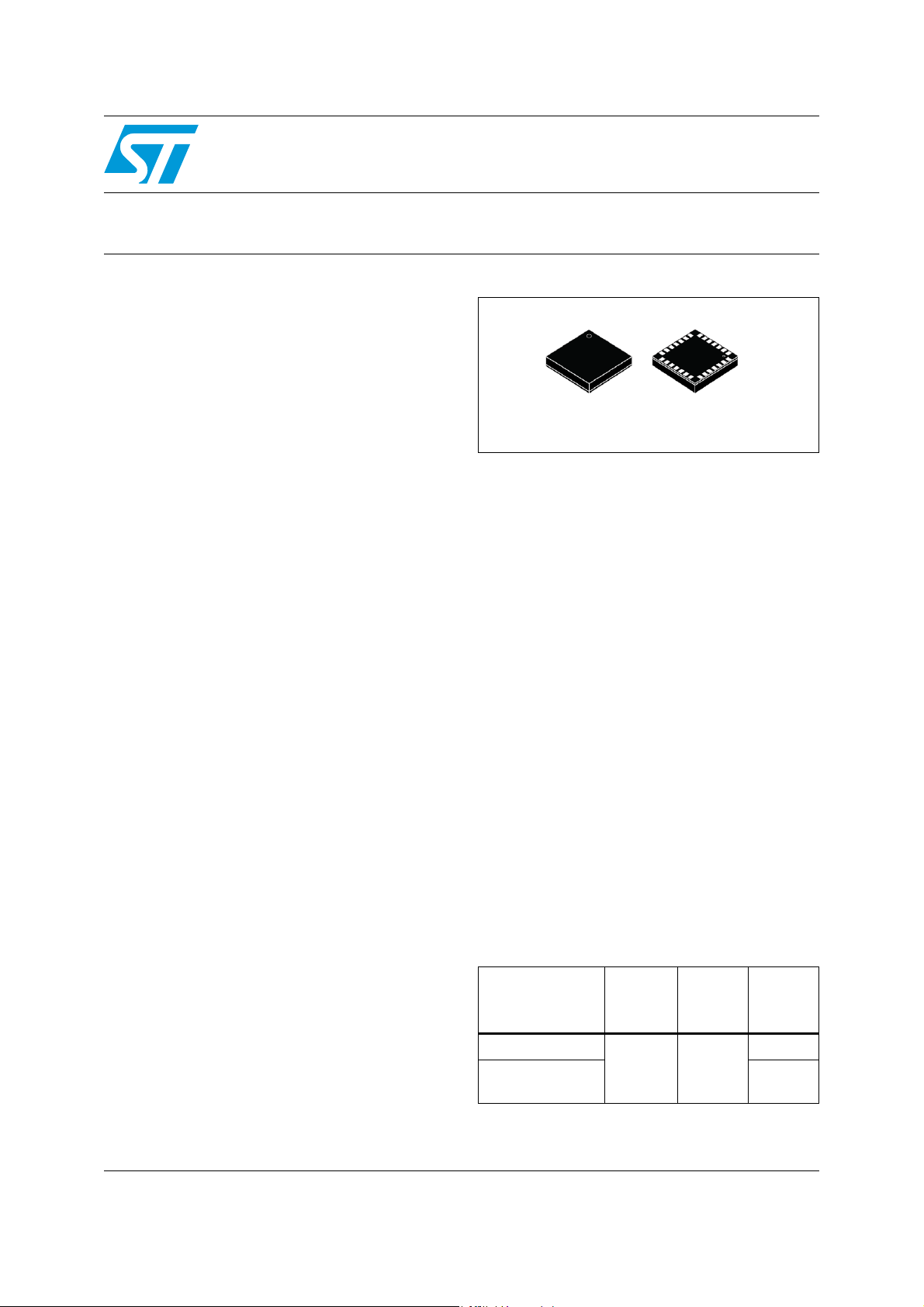
LGA-28L (5x5x1.0 mm)
The various sensing elements are manufactured
by using specialized micromachining processes,
while the IC interfaces are realized using a CMOS
technology that allows the design of a dedicated
circuit which is trimmed to better match the
sensing element characteristics. The
LSM303DLM has a linear acceleration full-scale
of ±2 g / ±4 g / ±8 g and a magnetic field full-scale
of ±1.3 / ±1.9 / ±2.5 / ±4.0 / ±4.7 / ±5.6 / ±8.1
gauss, both fully selectable by the user.
The LSM303DLM includes an I
interface that supports standard mode (100 kHz)
and fast mode (400 kHz). The system can be
configured to generate an interrupt signal by
inertial wakeup/free-fall events, as well as by the
position of the device itself. Thresholds and timing
of interrupt generators are programmable on the
fly by the end user.
Magnetic and accelerometer parts can be
enabled or put into power-down mode separately.
The LSM303DLM is available in a plastic land grid
array package (LGA), and is guaranteed to
operate over an extended temperature range from
-40 to +85 °C.
Table 1. Device summary
Temp.
Part number
range
[°C]
2
C serial bus
Package Packing
The LSM303DLM is a system-in-package
featuring a 3D digital linear acceleration sensor
and a 3D digital magnetic sensor.
April 2011 Doc ID 018725 Rev 1 1/38
This is preliminary information on a new product now in development or undergoing evaluation. Details are subject to
change without notice.
LSM303DLM
LSM303DLMTR
-40 to +85 LGA-28
Tr ay
Tape and
reel
www.st.com
38
Page 2

Contents LSM303DLM
Contents
1 Block diagram and pin description . . . . . . . . . . . . . . . . . . . . . . . . . . . . . 5
1.1 Block diagram . . . . . . . . . . . . . . . . . . . . . . . . . . . . . . . . . . . . . . . . . . . . . . . 5
1.2 Pin description . . . . . . . . . . . . . . . . . . . . . . . . . . . . . . . . . . . . . . . . . . . . . . 6
2 Module specifications . . . . . . . . . . . . . . . . . . . . . . . . . . . . . . . . . . . . . . . . 8
2.1 Sensor characteristics . . . . . . . . . . . . . . . . . . . . . . . . . . . . . . . . . . . . . . . . 8
2.2 Electrical characteristics . . . . . . . . . . . . . . . . . . . . . . . . . . . . . . . . . . . . . . . 9
2.3 Communication interface characteristics . . . . . . . . . . . . . . . . . . . . . . . . . 10
2.3.1 Sensor I2C - inter IC control interface . . . . . . . . . . . . . . . . . . . . . . . . . . 10
3 Absolute maximum ratings . . . . . . . . . . . . . . . . . . . . . . . . . . . . . . . . . . 11
4 Terminology . . . . . . . . . . . . . . . . . . . . . . . . . . . . . . . . . . . . . . . . . . . . . . . 12
4.1 Linear acceleration sensitivity . . . . . . . . . . . . . . . . . . . . . . . . . . . . . . . . . 12
4.2 Zero-g level . . . . . . . . . . . . . . . . . . . . . . . . . . . . . . . . . . . . . . . . . . . . . . . . 12
4.3 Sleep-to-wakeup . . . . . . . . . . . . . . . . . . . . . . . . . . . . . . . . . . . . . . . . . . . 12
5 Functionality . . . . . . . . . . . . . . . . . . . . . . . . . . . . . . . . . . . . . . . . . . . . . . 13
5.1 Factory calibration . . . . . . . . . . . . . . . . . . . . . . . . . . . . . . . . . . . . . . . . . . 13
6 Application hints . . . . . . . . . . . . . . . . . . . . . . . . . . . . . . . . . . . . . . . . . . . 14
6.1 External capacitors . . . . . . . . . . . . . . . . . . . . . . . . . . . . . . . . . . . . . . . . . . 14
6.2 Soldering information . . . . . . . . . . . . . . . . . . . . . . . . . . . . . . . . . . . . . . . . 15
6.3 High current wiring effects . . . . . . . . . . . . . . . . . . . . . . . . . . . . . . . . . . . . 15
7 Digital interfaces . . . . . . . . . . . . . . . . . . . . . . . . . . . . . . . . . . . . . . . . . . . 16
7.1 I2C serial interface . . . . . . . . . . . . . . . . . . . . . . . . . . . . . . . . . . . . . . . . . . 16
7.1.1 I2C operation . . . . . . . . . . . . . . . . . . . . . . . . . . . . . . . . . . . . . . . . . . . . . 17
7.1.2 Linear acceleration digital interface . . . . . . . . . . . . . . . . . . . . . . . . . . . . 18
7.1.3 Magnetic field digital interface . . . . . . . . . . . . . . . . . . . . . . . . . . . . . . . . 18
8 Register mapping . . . . . . . . . . . . . . . . . . . . . . . . . . . . . . . . . . . . . . . . . . 20
9 Register description . . . . . . . . . . . . . . . . . . . . . . . . . . . . . . . . . . . . . . . . 22
2/38 Doc ID 018725 Rev 1
Page 3

LSM303DLM Contents
9.1 Linear acceleration register description . . . . . . . . . . . . . . . . . . . . . . . . . . 22
9.1.1 CTRL_REG1_A (20h) . . . . . . . . . . . . . . . . . . . . . . . . . . . . . . . . . . . . . . 22
9.1.2 CTRL_REG2_A (21h) . . . . . . . . . . . . . . . . . . . . . . . . . . . . . . . . . . . . . . 23
9.1.3 CTRL_REG3_A (22h) . . . . . . . . . . . . . . . . . . . . . . . . . . . . . . . . . . . . . . 24
9.1.4 CTRL_REG4_A (23h) . . . . . . . . . . . . . . . . . . . . . . . . . . . . . . . . . . . . . . 25
9.1.5 CTRL_REG5_A (24h . . . . . . . . . . . . . . . . . . . . . . . . . . . . . . . . . . . . . . ) 26
9.1.6 HP_FILTER_RESET_A (25h) . . . . . . . . . . . . . . . . . . . . . . . . . . . . . . . . 26
9.1.7 REFERENCE_A (26h) . . . . . . . . . . . . . . . . . . . . . . . . . . . . . . . . . . . . . . 26
9.1.8 STATUS_REG_A(27h) . . . . . . . . . . . . . . . . . . . . . . . . . . . . . . . . . . . . . . 27
9.1.9 OUT_X_L_A (28h), OUT_X_H_A (29h) . . . . . . . . . . . . . . . . . . . . . . . . . 27
9.1.10 OUT_Y_L_A (2Ah), OUT_Y_H_A (2Bh) . . . . . . . . . . . . . . . . . . . . . . . . 27
9.1.11 OUT_Z_L_A (2Ch), OUT_Z_H_A (2Dh) . . . . . . . . . . . . . . . . . . . . . . . . 27
9.1.12 INT1_CFG_A (30h) . . . . . . . . . . . . . . . . . . . . . . . . . . . . . . . . . . . . . . . . 28
9.1.13 INT1_SRC_A (31h) . . . . . . . . . . . . . . . . . . . . . . . . . . . . . . . . . . . . . . . . 29
9.1.14 INT1_THS_A (32h) . . . . . . . . . . . . . . . . . . . . . . . . . . . . . . . . . . . . . . . . 29
9.1.15 INT1_DURATION_A (33h) . . . . . . . . . . . . . . . . . . . . . . . . . . . . . . . . . . . 29
9.1.16 INT2_CFG_A (34h) . . . . . . . . . . . . . . . . . . . . . . . . . . . . . . . . . . . . . . . . 30
9.1.17 INT2_SRC_A (35h) . . . . . . . . . . . . . . . . . . . . . . . . . . . . . . . . . . . . . . . . 31
9.1.18 INT2_THS_A (36h) . . . . . . . . . . . . . . . . . . . . . . . . . . . . . . . . . . . . . . . . 31
9.1.19 INT2_DURATION_A (37h) . . . . . . . . . . . . . . . . . . . . . . . . . . . . . . . . . . . 32
9.2 Magnetic field sensing register description . . . . . . . . . . . . . . . . . . . . . . . 32
9.2.1 CRA_REG_M (00h) . . . . . . . . . . . . . . . . . . . . . . . . . . . . . . . . . . . . . . . . 32
9.2.2 CRB_REG_M (01h) . . . . . . . . . . . . . . . . . . . . . . . . . . . . . . . . . . . . . . . . 32
9.2.3 MR_REG_M (02h) . . . . . . . . . . . . . . . . . . . . . . . . . . . . . . . . . . . . . . . . . 33
9.2.4 OUT_X_H_M (03), OUT_X_LH_M (04h) . . . . . . . . . . . . . . . . . . . . . . . . 33
9.2.5 OUT_Z_H_M (05), OUT_Z_L_M (06h) . . . . . . . . . . . . . . . . . . . . . . . . . 34
9.2.6 OUT_Y_H_M (07), OUT_Y_L_M (08h) . . . . . . . . . . . . . . . . . . . . . . . . . 34
9.2.7 SR_REG_M (09h) . . . . . . . . . . . . . . . . . . . . . . . . . . . . . . . . . . . . . . . . . 34
9.2.8 IR_REG_M (0Ah/0Bh/0Ch) . . . . . . . . . . . . . . . . . . . . . . . . . . . . . . . . . . 34
9.2.9 WHO_AM_I _M (0F) . . . . . . . . . . . . . . . . . . . . . . . . . . . . . . . . . . . . . . . 34
10 Package information . . . . . . . . . . . . . . . . . . . . . . . . . . . . . . . . . . . . . . . . 35
11 Revision history . . . . . . . . . . . . . . . . . . . . . . . . . . . . . . . . . . . . . . . . . . . 36
Doc ID 018725 Rev 1 3/38
Page 4

List of tables LSM303DLM
List of tables
Table 1. Device summary . . . . . . . . . . . . . . . . . . . . . . . . . . . . . . . . . . . . . . . . . . . . . . . . . . . . . . . . . . 1
Table 2. Pin description . . . . . . . . . . . . . . . . . . . . . . . . . . . . . . . . . . . . . . . . . . . . . . . . . . . . . . . . . . . 5
Table 3. Sensor characteristics . . . . . . . . . . . . . . . . . . . . . . . . . . . . . . . . . . . . . . . . . . . . . . . . . . . . . 7
Table 4. Electrical characteristics . . . . . . . . . . . . . . . . . . . . . . . . . . . . . . . . . . . . . . . . . . . . . . . . . . . . 8
Table 5. I
Table 6. Absolute maximum ratings . . . . . . . . . . . . . . . . . . . . . . . . . . . . . . . . . . . . . . . . . . . . . . . . . 10
Table 7. Serial interface pin description . . . . . . . . . . . . . . . . . . . . . . . . . . . . . . . . . . . . . . . . . . . . . . 15
Table 8. Serial interface pin description . . . . . . . . . . . . . . . . . . . . . . . . . . . . . . . . . . . . . . . . . . . . . . 15
Table 9. Transfer when master is writing one byte to slave . . . . . . . . . . . . . . . . . . . . . . . . . . . . . . . 16
Table 10. Transfer when master is writing multiple bytes to slave . . . . . . . . . . . . . . . . . . . . . . . . . . . 16
Table 11. Transfer when master is receiving (reading) one byte of data from slave . . . . . . . . . . . . . 16
Table 12. SAD and read/write patterns. . . . . . . . . . . . . . . . . . . . . . . . . . . . . . . . . . . . . . . . . . . . . . . . 17
Table 13. Transfer when master is receiving (reading) multiple bytes of data from slave . . . . . . . . . 17
Table 14. SAD and read/write patterns. . . . . . . . . . . . . . . . . . . . . . . . . . . . . . . . . . . . . . . . . . . . . . . . 17
Table 15. Register address map. . . . . . . . . . . . . . . . . . . . . . . . . . . . . . . . . . . . . . . . . . . . . . . . . . . . . 19
Table 16. CTRL_REG1_A register . . . . . . . . . . . . . . . . . . . . . . . . . . . . . . . . . . . . . . . . . . . . . . . . . . . 21
Table 17. CTRL_REG1_A description . . . . . . . . . . . . . . . . . . . . . . . . . . . . . . . . . . . . . . . . . . . . . . . . 21
Table 18. Power mode and low-power output data rate configurations . . . . . . . . . . . . . . . . . . . . . . . 21
Table 19. Normal-mode output data rate configurations and low-pass cut-off frequencies . . . . . . . . 22
Table 20. CTRL_REG2_A register . . . . . . . . . . . . . . . . . . . . . . . . . . . . . . . . . . . . . . . . . . . . . . . . . . . 22
Table 21. CTRL_REG2_A description . . . . . . . . . . . . . . . . . . . . . . . . . . . . . . . . . . . . . . . . . . . . . . . . 22
Table 22. High-pass filter mode configuration . . . . . . . . . . . . . . . . . . . . . . . . . . . . . . . . . . . . . . . . . . 23
Table 23. High-pass filter cut-off frequency configuration . . . . . . . . . . . . . . . . . . . . . . . . . . . . . . . . . 23
Table 24. CTRL_REG3_A register . . . . . . . . . . . . . . . . . . . . . . . . . . . . . . . . . . . . . . . . . . . . . . . . . . . 23
Table 25. CTRL_REG3_A description . . . . . . . . . . . . . . . . . . . . . . . . . . . . . . . . . . . . . . . . . . . . . . . . 23
Table 26. Data signal on INT 1 and INT 2 pad . . . . . . . . . . . . . . . . . . . . . . . . . . . . . . . . . . . . . . . . . . 24
Table 27. CTRL_REG4_A register . . . . . . . . . . . . . . . . . . . . . . . . . . . . . . . . . . . . . . . . . . . . . . . . . . . 24
Table 28. CTRL_REG4_A description . . . . . . . . . . . . . . . . . . . . . . . . . . . . . . . . . . . . . . . . . . . . . . . . 24
Table 29. CTRL_REG5_A register . . . . . . . . . . . . . . . . . . . . . . . . . . . . . . . . . . . . . . . . . . . . . . . . . . . 25
Table 30. CTRL_REG5_A description . . . . . . . . . . . . . . . . . . . . . . . . . . . . . . . . . . . . . . . . . . . . . . . . 25
Table 31. Sleep-to-wakeup configuration . . . . . . . . . . . . . . . . . . . . . . . . . . . . . . . . . . . . . . . . . . . . . . 25
Table 32. REFERENCE_A register . . . . . . . . . . . . . . . . . . . . . . . . . . . . . . . . . . . . . . . . . . . . . . . . . . 25
Table 33. REFERENCE_A description. . . . . . . . . . . . . . . . . . . . . . . . . . . . . . . . . . . . . . . . . . . . . . . . 25
Table 34. STATUS_REG_A register . . . . . . . . . . . . . . . . . . . . . . . . . . . . . . . . . . . . . . . . . . . . . . . . . 26
Table 35. STATUS_REG_A description . . . . . . . . . . . . . . . . . . . . . . . . . . . . . . . . . . . . . . . . . . . . . . . 26
Table 36. INT1_CFG_A register . . . . . . . . . . . . . . . . . . . . . . . . . . . . . . . . . . . . . . . . . . . . . . . . . . . . . 27
Table 37. INT1_CFG_A description . . . . . . . . . . . . . . . . . . . . . . . . . . . . . . . . . . . . . . . . . . . . . . . . . . 27
Table 38. Interrupt 1 source configurations . . . . . . . . . . . . . . . . . . . . . . . . . . . . . . . . . . . . . . . . . . . . 27
Table 39. INT1_SRC register . . . . . . . . . . . . . . . . . . . . . . . . . . . . . . . . . . . . . . . . . . . . . . . . . . . . . . . 28
Table 40. INT1_SRC_A description . . . . . . . . . . . . . . . . . . . . . . . . . . . . . . . . . . . . . . . . . . . . . . . . . . 28
Table 41. INT1_THS register . . . . . . . . . . . . . . . . . . . . . . . . . . . . . . . . . . . . . . . . . . . . . . . . . . . . . . . 28
Table 42. INT1_THS description . . . . . . . . . . . . . . . . . . . . . . . . . . . . . . . . . . . . . . . . . . . . . . . . . . . . 28
Table 43. INT1_DURATION_A register . . . . . . . . . . . . . . . . . . . . . . . . . . . . . . . . . . . . . . . . . . . . . . . 28
Table 44. INT2_DURATION_A description . . . . . . . . . . . . . . . . . . . . . . . . . . . . . . . . . . . . . . . . . . . . 29
Table 45. INT2_CFG_A register . . . . . . . . . . . . . . . . . . . . . . . . . . . . . . . . . . . . . . . . . . . . . . . . . . . . . 29
Table 46. INT2_CFG_A description . . . . . . . . . . . . . . . . . . . . . . . . . . . . . . . . . . . . . . . . . . . . . . . . . . 29
Table 47. Interrupt mode configuration . . . . . . . . . . . . . . . . . . . . . . . . . . . . . . . . . . . . . . . . . . . . . . . . 29
Table 48. INT2_SRC_A register . . . . . . . . . . . . . . . . . . . . . . . . . . . . . . . . . . . . . . . . . . . . . . . . . . . . . 30
2
C slave timing values . . . . . . . . . . . . . . . . . . . . . . . . . . . . . . . . . . . . . . . . . . . . . . . . . . . . . 9
4/38 Doc ID 018725 Rev 1
Page 5

LSM303DLM List of tables
Table 49. INT2_SRC_A description . . . . . . . . . . . . . . . . . . . . . . . . . . . . . . . . . . . . . . . . . . . . . . . . . . 30
Table 50. INT2_THS register . . . . . . . . . . . . . . . . . . . . . . . . . . . . . . . . . . . . . . . . . . . . . . . . . . . . . . . 30
Table 51. INT2_THS description . . . . . . . . . . . . . . . . . . . . . . . . . . . . . . . . . . . . . . . . . . . . . . . . . . . . 30
Table 52. INT2_DURATION_A register . . . . . . . . . . . . . . . . . . . . . . . . . . . . . . . . . . . . . . . . . . . . . . . 31
Table 53. INT2_DURATION_A description . . . . . . . . . . . . . . . . . . . . . . . . . . . . . . . . . . . . . . . . . . . . 31
Table 54. CRA_REG_M register . . . . . . . . . . . . . . . . . . . . . . . . . . . . . . . . . . . . . . . . . . . . . . . . . . . . 31
Table 55. CRA_REG_M description . . . . . . . . . . . . . . . . . . . . . . . . . . . . . . . . . . . . . . . . . . . . . . . . . . 31
Table 56. Data rate configurations . . . . . . . . . . . . . . . . . . . . . . . . . . . . . . . . . . . . . . . . . . . . . . . . . . . 31
Table 57. CRA_REG register . . . . . . . . . . . . . . . . . . . . . . . . . . . . . . . . . . . . . . . . . . . . . . . . . . . . . . . 31
Table 58. Gain setting. . . . . . . . . . . . . . . . . . . . . . . . . . . . . . . . . . . . . . . . . . . . . . . . . . . . . . . . . . . . . 32
Table 59. MR_REG . . . . . . . . . . . . . . . . . . . . . . . . . . . . . . . . . . . . . . . . . . . . . . . . . . . . . . . . . . . . . . 32
Table 60. MR_REG description . . . . . . . . . . . . . . . . . . . . . . . . . . . . . . . . . . . . . . . . . . . . . . . . . . . . . 32
Table 61. Magnetic sensor operating mode . . . . . . . . . . . . . . . . . . . . . . . . . . . . . . . . . . . . . . . . . . . . 32
Table 62. SR register . . . . . . . . . . . . . . . . . . . . . . . . . . . . . . . . . . . . . . . . . . . . . . . . . . . . . . . . . . . . . 33
Table 63. SR register description . . . . . . . . . . . . . . . . . . . . . . . . . . . . . . . . . . . . . . . . . . . . . . . . . . . . 33
Table 64. IRA_REG_M . . . . . . . . . . . . . . . . . . . . . . . . . . . . . . . . . . . . . . . . . . . . . . . . . . . . . . . . . . . . 33
Table 65. IRB_REG_M . . . . . . . . . . . . . . . . . . . . . . . . . . . . . . . . . . . . . . . . . . . . . . . . . . . . . . . . . . . . 33
Table 66. IRC_REG_M . . . . . . . . . . . . . . . . . . . . . . . . . . . . . . . . . . . . . . . . . . . . . . . . . . . . . . . . . . . . 33
Table 67. WHO_AM_I_M . . . . . . . . . . . . . . . . . . . . . . . . . . . . . . . . . . . . . . . . . . . . . . . . . . . . . . . . . . 33
Table 68. Revision history . . . . . . . . . . . . . . . . . . . . . . . . . . . . . . . . . . . . . . . . . . . . . . . . . . . . . . . . . 35
Doc ID 018725 Rev 1 5/38
Page 6
Block diagram and pin description LSM303DLM
1 Block diagram and pin description
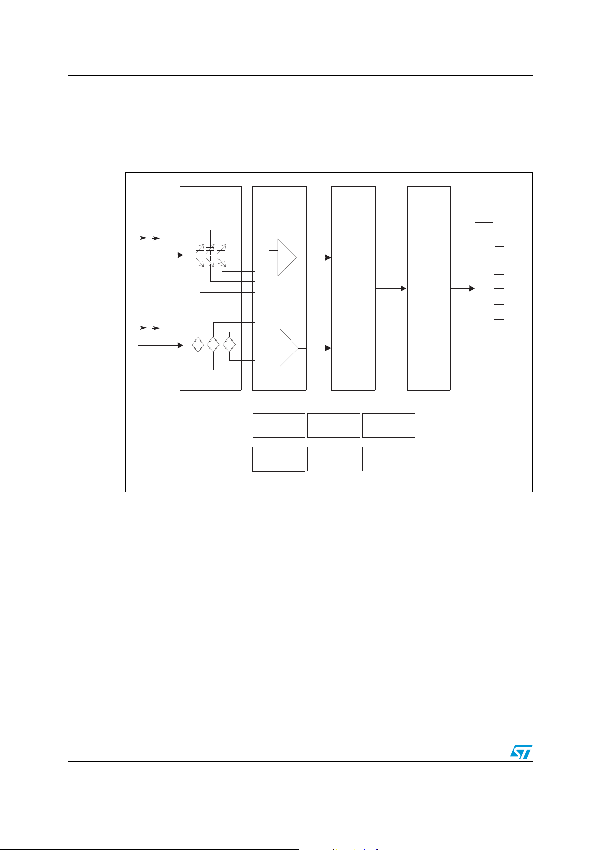
1.1 Block diagram
Figure 1. Block diagram
I (a)
I (M)
Sensing Block
X+
Y+
Z+
Z-
Y-
X-
X+
Y+
Z+
Z-
Y-
X-
Sensing Interface
CHARGE
AMPLIFIER
+
MUX
-
CHARGE
AMPLIFIER
+
MUX
-
INTERRUPT GEN.
CLOCK
converter
REFERENCE
OFFSET
CIRCUITS
A/D Control
TRIMMING
CIRCUITS
BUILT-IN
SET/RESET
CIRCUITS
Logic
DI
I2C
SDA_A
SCL_A
SDA_M
SCL_M
INT1
INT2
AM09239V1
6/38 Doc ID 018725 Rev 1
Page 7
LSM303DLM Block diagram and pin description
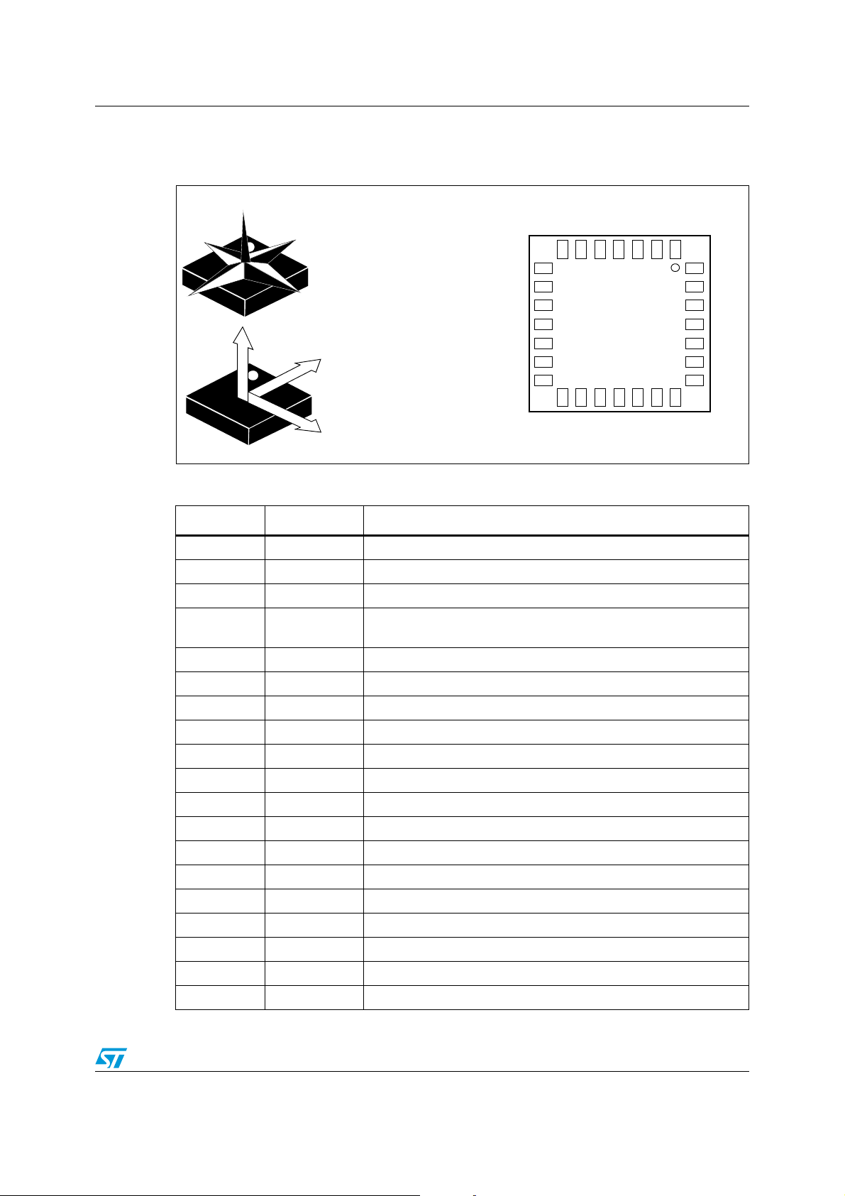
1.2 Pin description
Figure 2. Pin connection
:
3#,?!
2%3
3$!?!
).4
2%3
).4
&),46$$
&),4).9
2%3
2%3
2%3
2%3
2%3
'.$
2%3
3!?!
.#
6$$
2%3
!-V
8
:
9
$)2%#4)/./&
$%4%#4!",%
-!'.%4)#&)%,$3
9
$)2%#4)/./&
$%4%#4!",%
!##%,%2!4)/.3
8
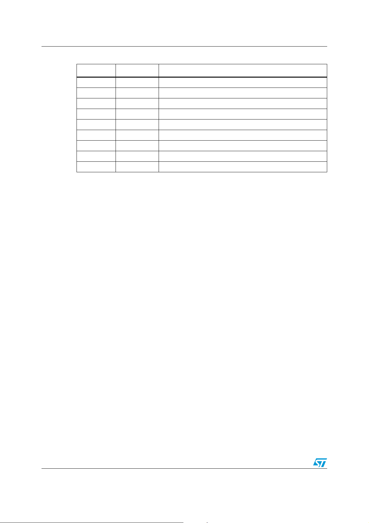
Table 2. Pin description
.#
3#,?-
3$!?-
$2$9?-
2%3
3%4
6DD?)/
,3-$-
"/44/-6)%7
#
2%3
2%3
3%4
Pin# Name Function
1 Reserved Connect to GND
2 GND 0 V supply
3 Reserved Connect to GND
4 SA0_A
Linear acceleration signal I2C less significant bit of the device
address (SA0)
5 NC Internally not connected
6VddPower supply
7 Reserved Connect to Vdd
8 Reserved Leave unconnected
9 Reserved Leave unconnected
10 Reserved Leave unconnected
11 Reserved Leave unconnected
12 SET2 S/R capacitor connection (C2)
13 Reserved Leave unconnected
14 Reserved Leave unconnected
15 C1 Reserved capacitor connection (C1)
16 SET1 S/R capacitor connection (C2)
17 Reserved Connect to GND
18 DRDY_M Magnetic signal interface data ready
2
19 SDA_M Magnetic signal interface I
C serial data (SDA)
Doc ID 018725 Rev 1 7/38
Page 8
Block diagram and pin description LSM303DLM
Table 2. Pin description (continued)
Pin# Name Function
20 SCL_M Magnetic signal interface I2C serial clock (SCL)
21 NC Internally not connected
22 Vdd_IO Signal interface power supply for I/O pins
23 Reserved Connect to Vdd_IO
24 SCL_A Linear acceleration signal interface I2C serial clock (SCL)
2
25 SDA_A Linear acceleration signal interface I
26 INT1 Inertial Interrupt 1
27 INT2 Inertial Interrupt 2
28 Reserved Connect to GND
C serial data (SDA)
8/38 Doc ID 018725 Rev 1
Page 9
LSM303DLM Module specifications
2 Module specifications
2.1 Sensor characteristics
@ Vdd = 2.5 V, T = 25 °C unless otherwise noted
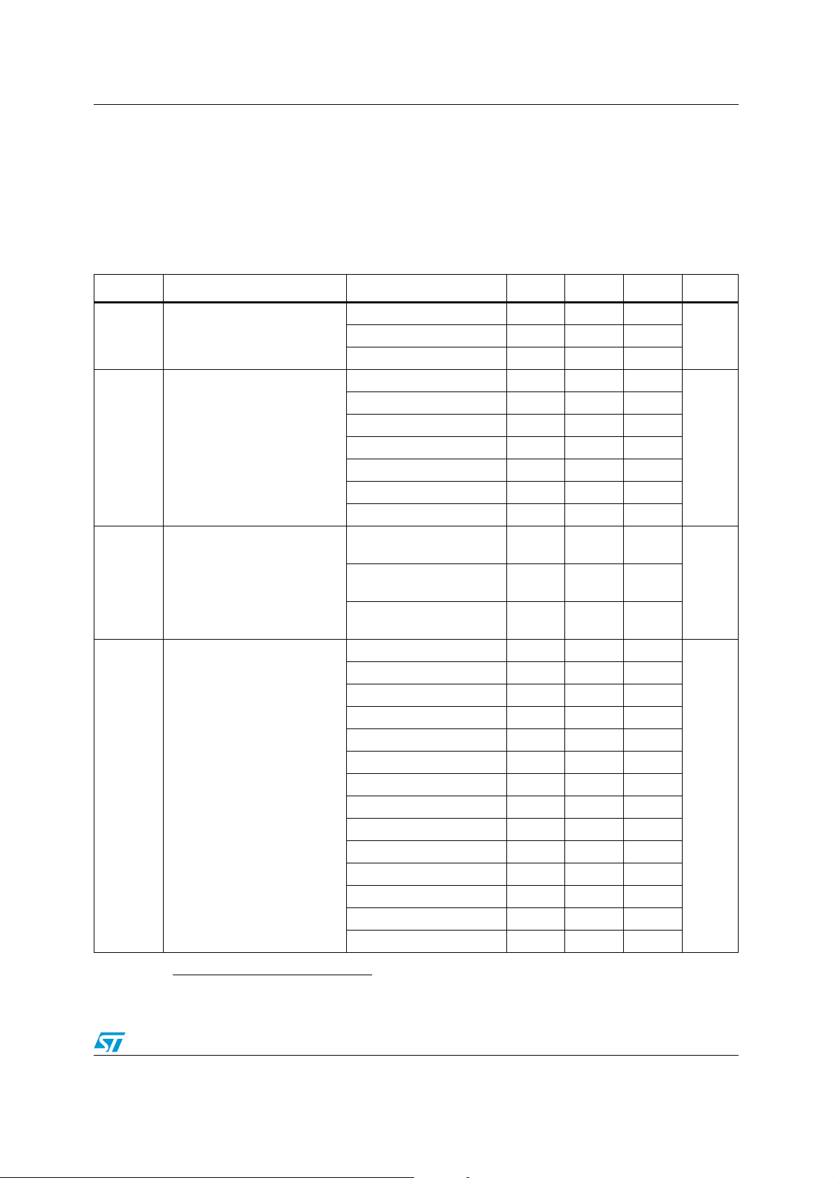
Table 3. Sensor characteristics
Symbol Parameter Test conditions Min. Typ.
FS bit set to 00 ±2.0
LA_FS
M_FS Magnetic measurement range
LA_So Linear acceleration sensitivity
M_GN Magnetic gain setting
Linear acceleration
measurement range
(2)
FS bit set to 11 ±8.0
GN bits set to 001 ±1.3
GN bits set to 010 ±1.9
GN bits set to 011 ±2.5
GN bits set to 100 ±4.0
GN bits set to 101 ±4.7
GN bits set to 110 ±5.6
GN bits set to 111 ±8.1
FS bit set to 00
12-bit representation
FS bit set to 01
12-bit representation
FS bit set to 11
12-bit representation
GN bits set to 001 (X,Y) 1100
GN bits set to 001 (Z) 980
GN bits set to 010 (X,Y) 855
GN bits set to 010 (Z) 760
GN bits set to 011 (X,Y) 670
GN bits set to 011 (Z) 600
GN bits set to 100 (X,Y) 450
GN bits set to 100 (Z) 400
GN bits set to 101 (X,Y) 400
GN bits set to 101 (Z) 355
GN bits set to 110 (X,Y) 330
GN bits set to 110 (Z) 295
GN bits set to 111
GN bits set to 111
(a)
.
(2)
(X,Y) 230
(2)
(Z) 205
1
2
3.9
(1)
Max. Unit
gFS bit set to 01 ±4.0
gauss
g/digit
m
LSB/
gauss
a. The product is factory calibrated at 2.5 V. The operational power supply range is from 2.16 V to 3.6 V.
Doc ID 018725 Rev 1 9/38
Page 10
Module specifications LSM303DLM
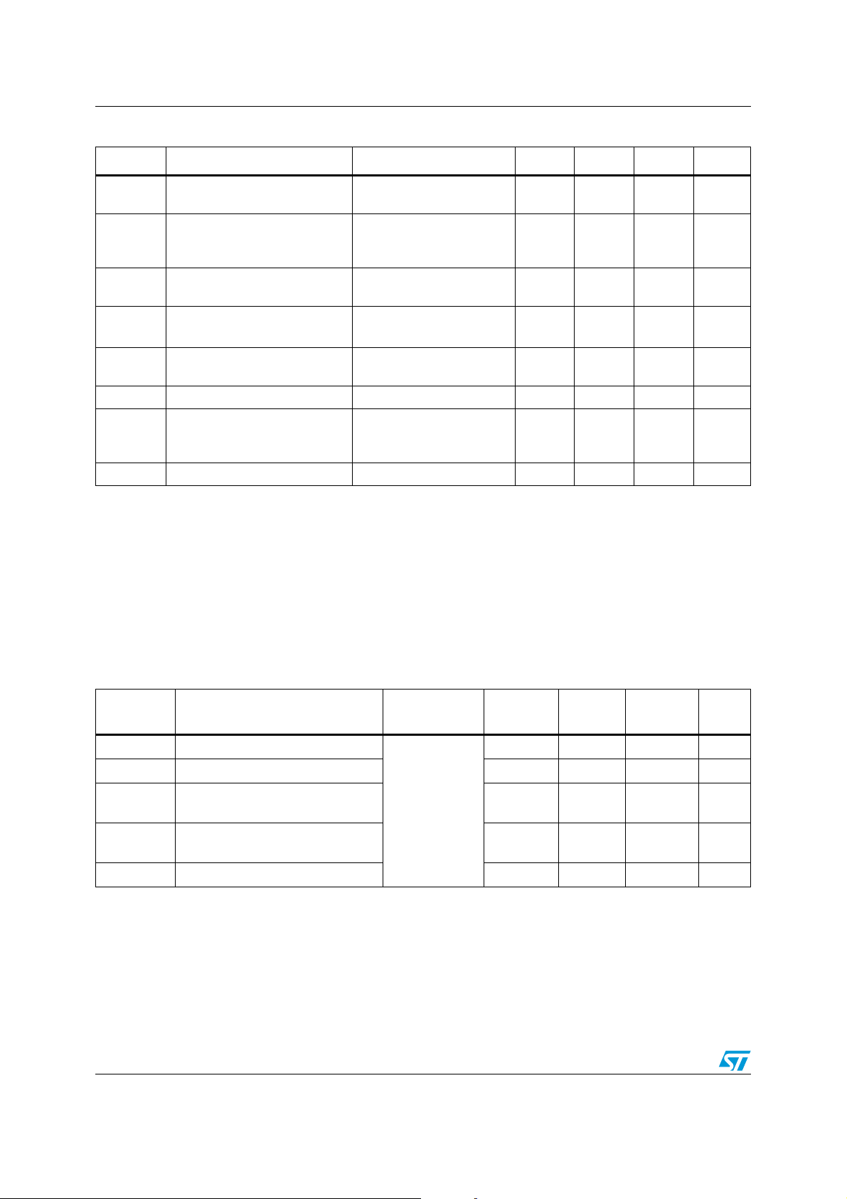
Table 3. Sensor characteristics (continued)
Symbol Parameter Test conditions Min. Typ.
(1)
Max. Unit
LA_TCSo
Linear acceleration sensitivity
change vs. temperature
FS bit set to 00 ±0.01 %/°C
Linear acceleration typical
LA_TyOff
LA_TCOff
Zero-g level offset
accuracy
(3),(4)
Linear acceleration Zero-g level
change vs. temperature
M_CAS Magnetic cross-axis sensitivity
M_EF Maximum exposed field
FS bit set to 00 ±60 mg
Max. delta from 25 °C ±0.5 mg/°C
Cross field = 0.5 gauss
H applied = ±3 gauss
No permitting effect on
zero reading
±1
10000 gauss
M_R Magnetic resolution 5 mgauss
Sensitivity starts to
M_DF Disturbing field
degrade. Use S/R pulse to
20 gauss
restore sensitivity
Top Operating temperature range -40 +85 °C
1. Typical specifications are not guaranteed.
2. Verified by wafer level test and measurement of initial offset and sensitivity.
3. Typical Zero-g level offset value after MSL3 preconditioning.
4. Offset can be eliminated by enabling the built-in high-pass filter.
%FS/
gauss
2.2 Electrical characteristics
@ Vdd = 2.5 V, T = 25 °C unless otherwise noted.
Table 4. Electrical characteristics
Symbol Parameter
Vdd Supply voltage
Tes t
conditions
Min. Typ.
2.16 3.6 V
Vdd_IO Module power supply for I/O 1.71 1.8 Vdd+0.1 V
Idd
IddPdn
Current consumption in normal
(2)
mode
Current consumption in powerdown mode
-
Top Operating temperature range -40 +85
1. Typical specifications are not guaranteed.
2. Magnetic sensor setting ODR = 7.5 Hz. Accelerometer sensor ODR = 50 Hz.
(1)
Max. Unit
360 µA
2µA
°C
10/38 Doc ID 018725 Rev 1
Page 11
LSM303DLM Module specifications
W
W
W
W
W
W
W
W
W
W
W
W
2.3 Communication interface characteristics
2.3.1 Sensor I2C - inter IC control interface
Subject to general operating conditions for Vdd and top.
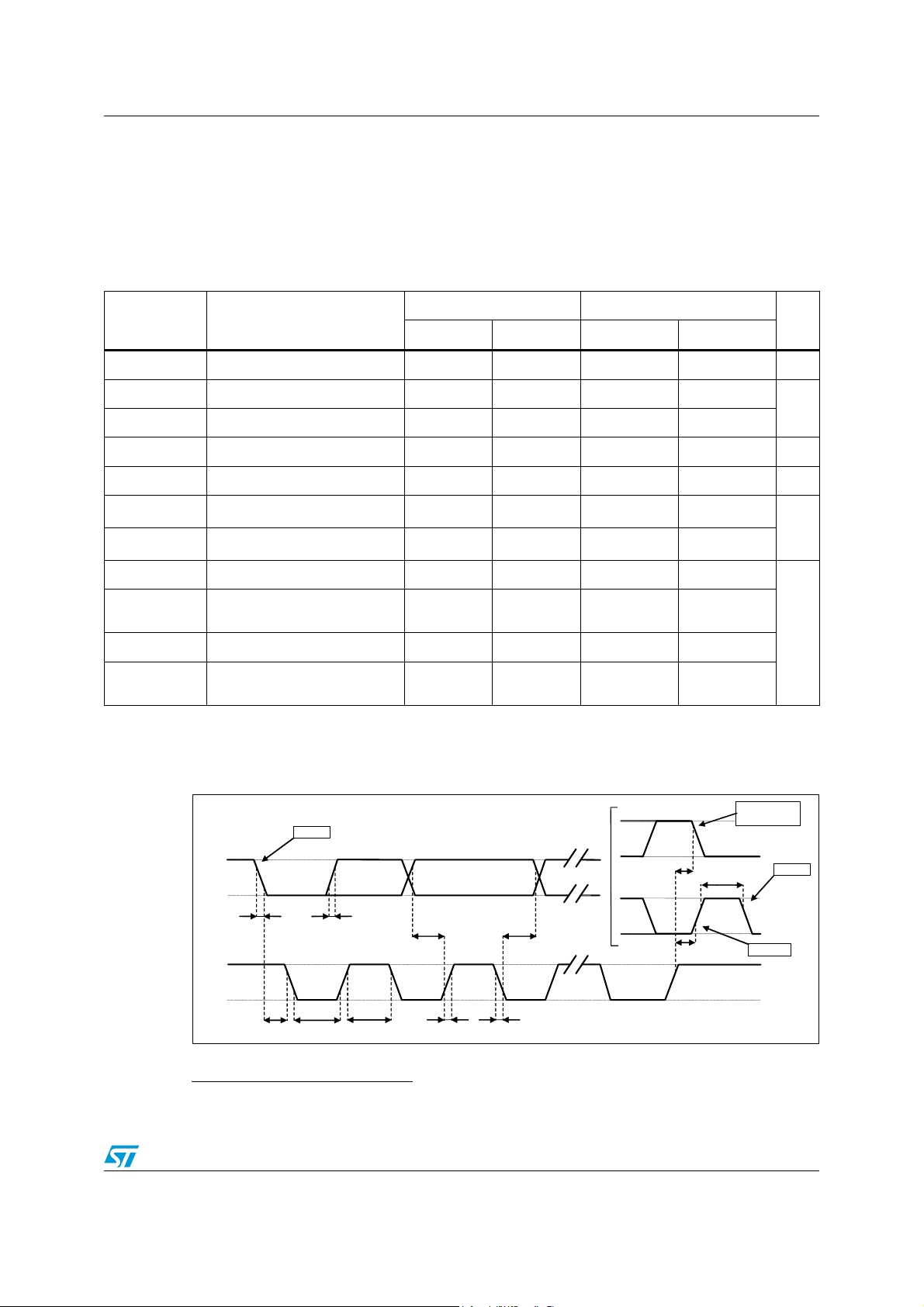
Table 5. I2C slave timing values
Symbol Parameter
2
C standard mode
I
Min. Max. Min. Max.
(1)
I2C fast mode
(1)
Unit
f
(SCL)
t
w(SCLL)
t
w(SCLH)
t
su(SDA)
t
h(SDA)
t
r(SDA) tr(SCL)
t
f(SDA) tf(SCL)
t
h(ST)
t
su(SR)
t
su(SP)
t
w(SP:SR)
SCL clock frequency 0 100 0 400 KHz
SCL clock low time 4.7 1.3
SCL clock high time 4.0 0.6
SDA setup time 250 100 ns
SDA data hold time 0.01 3.45 0.01 0.9 µs
SDA and SCL rise time 1000
SDA and SCL fall time 300
START condition hold time 4 0.6
Repeated START condition
setup time
4.7 0.6
STOP condition setup time 4 0.6
Bus free time between STOP
and START condition
4.7 1.3
1. Data based on standard I2C protocol requirement, not tested in production.
2. Cb = total capacitance of one bus line, in pF.
Figure 3. I
2
C slave timing diagram
67$57
(b)
20 + 0.1C
20 + 0.1C
µs
(2)
b
(2)
b
300
ns
300
µs
5(3($7('
67$57
6'$
6&/
I6'$
K67
Z6&//
U6'$
Z6&/+
VX6'$
U6&/
VX65
Z6365
K6'$
VX63
I6&/
67$57
6723
b. Measurement points are done at 0.2·Vdd_IO and 0.8·Vdd_IO, for both ports.
Doc ID 018725 Rev 1 11/38
Page 12
Absolute maximum ratings LSM303DLM
3 Absolute maximum ratings
Stresses above those listed as “absolute maximum ratings” may cause permanent damage
to the device. This is a stress rating only and functional operation of the device under these
conditions is not implied. Exposure to maximum rating conditions for extended periods may
affect device reliability.
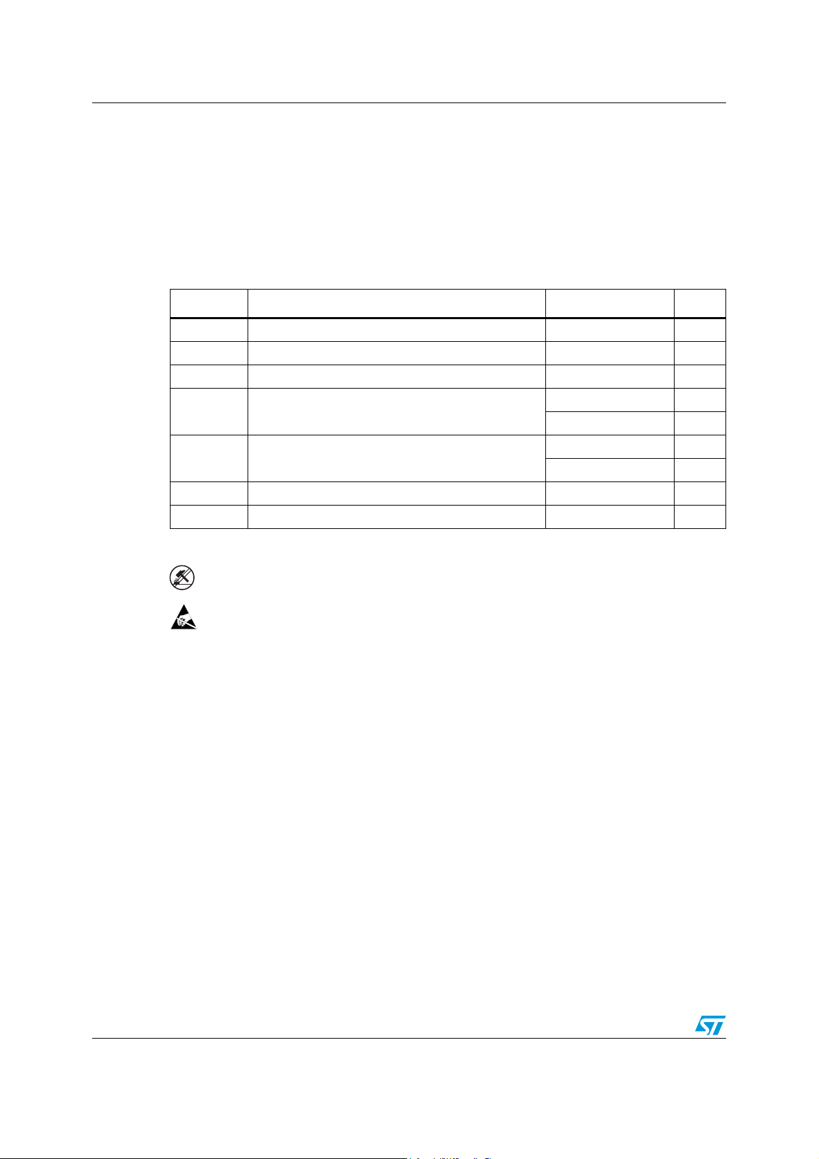
Table 6. Absolute maximum ratings
Symbol Ratings Maximum value Unit
Vdd Supply voltage -0.3 to 4.8 V
Vdd_IO I/O pins supply voltage -0.3 to 4.8 V
Vin Input voltage on any control pin (SCL, SDA) -0.3 to Vdd_IO +0.3 V
A
POW
A
UNP
T
OP
T
STG
Acceleration (any axis, powered, Vdd = 2.5 V)
Acceleration (any axis, unpowered)
Operating temperature range -40 to +85 °C
Storage temperature range -40 to +125 °C
3,000 for 0.5 ms g
10,000 for 0.1 ms g
3,000 for 0.5 ms g
10,000 for 0.1 ms g
This is a mechanical shock sensitive device, improper handling can cause permanent
damage to the part.
This is an ESD sensitive device, improper handling can cause permanent damage to
the part.
12/38 Doc ID 018725 Rev 1
Page 13

LSM303DLM Terminology
4 Terminology
4.1 Linear acceleration sensitivity
Linear acceleration sensitivity describes the gain of the accelerometer sensor and can be
determined by applying 1 g acceleration to it. As the sensor can measure DC accelerations,
this can be done easily by pointing the selected axis towards the ground, noting the output
value, rotating the sensor 180 degrees (pointing to the sky) and noting the output value
again. By doing so, a ±1 g acceleration is applied to the sensor. Subtracting the larger
output value from the smaller one, and dividing the result by 2, leads to the actual sensitivity
of the sensor. This value changes very little over temperature and over time. The sensitivity
tolerance describes the range of sensitivities of a large number of sensors.
4.2 Zero-g level
Zero-g level Offset (LA_TyOff) describes the deviation of an actual output signal from the
ideal output signal if no linear acceleration is present. A sensor in steady-state on a
horizontal surface measures 0 g on both the X and Y axes, whereas the Z axis measures 1
g. Ideally, the output is in the middle of the dynamic range of the sensor (content of OUT
registers 00h, data expressed as 2’s complement number). A deviation from the ideal value
in this case is called Zero-g offset. Offset is, to some extent, a result of stress to the MEMS
sensor and therefore the offset can slightly change after mounting the sensor onto a printed
circuit board or exposing it to extensive mechanical stress. Offset changes little over
temperature, see “Linear acceleration Zero-g level change vs. temperature” (LA_TCOff) in
Table 3. The Zero-g level tolerance (TyOff) describes the standard deviation of the range of
Zero-g levels of a group of sensors.
4.3 Sleep-to-wakeup
The “sleep-to-wakeup” function, in conjunction with low-power mode, allows further
reduction of system power consumption and the development of new smart applications.
The LSM303DLM may be set to a low-power operating mode, characterized by lower data
rate refreshing. In this way, the device, even if sleeping, continues sensing acceleration and
generating interrupt requests.
When the sleep-to-wakeup function is activated, the LSM303DLM is able to automatically
wake up as soon as the interrupt event has been detected, increasing the output data rate
and bandwidth. With this feature the system may be efficiently switched from low-power
mode to full-performance depending on user-selectable positioning and acceleration events,
therefore ensuring power-saving and flexibility.
Doc ID 018725 Rev 1 13/38
Page 14

Functionality LSM303DLM
5 Functionality
The LSM303DLM is a system-in-package featuring a 3D digital linear acceleration and 3D
digital magnetic field detection sensor.
The system includes specific sensing elements and an IC interface capable of measuring
both the linear acceleration and the magnetic field applied on it and to provide a signal to the
external world through an I
The sensing system is manufactured using specialized micromachining processes, while
the IC interfaces are realized using a CMOS technology that allows the design of a
dedicated circuit which is trimmed to better match the sensing element characteristics.
The LSM303DLM features two data-ready signals (RDY) which indicate when a new set of
measured acceleration data and magnetic data are available, therefore simplifying data
synchronization in the digital system that uses the device.
The LSM303DLM may also be configured to generate an inertial wakeup and free-fall
interrupt signal according to a programmed acceleration event along the enabled axes. Both
free-fall and wakeup can be used simultaneously on two different accelerometer interrupts.
2
C serial interface with separated digital output.
5.1 Factory calibration
The IC interface is factory calibrated for linear acceleration sensitivity (LA_So), and linear
acceleration Zero-g level (LA_TyOff).
The trimming values are stored inside the device in non-volatile memory. When the device is
turned on, the trimming parameters are downloaded into the registers to be used during
normal operation. This allows the use of the device without further calibration.
14/38 Doc ID 018725 Rev 1
Page 15
LSM303DLM Application hints
6 Application hints
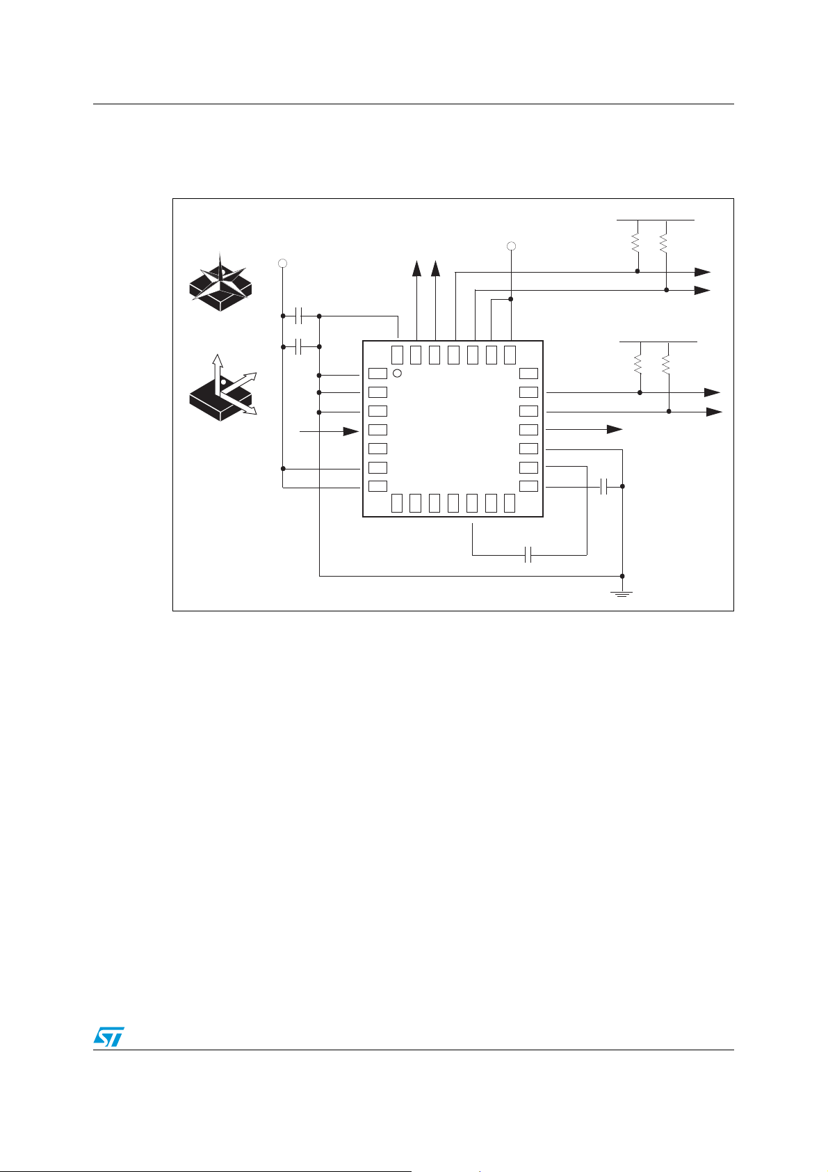
Figure 4. LSM303DLM electrical connection - recommended for I2C fast mode
Vdd_IO
SDA_A
SCL_A
Vdd_IO
Vdd_IO
RES
22
Rpu
Rpu=10kOhm
Vdd_IO
Rpu
NC
21
SCL_M
SDA_M
DRDY_M
RES
SET1
C1
15
418
C1=4.7uF
Rpu=10kOhm
Electrical connection
Z
1
DIRECTIONS OF
DETECTABLE
MAGNETIC FIELDS
Z
1
DIRECTIONS OF
DETECTABLE
ACCELERATIONS
Vdd
Y
C3 = 10uF
X
C4 = 100uF
Y
X
RES
GND
GND
SA0
VDD
RES
RES
INT2
INT1
28
1
LSM303DLM
NC
7
(TOP VIEW)
6.1 External capacitors
The C1 and C2 external capacitors should have a low SR value ceramic type construction.
Reservoir capacitor C1 is nominally 4.7 µF in capacitance, with the set/reset capacitor C2
nominally 0.22 µF in capacitance.
The device core is supplied through the Vdd line. Power supply decoupling capacitors
(C4=100 nF ceramic, C3=10 µF Al) should be placed as near as possible to the supply pin
of the device (common design practice). All the voltage and ground supplies must be
present at the same time to obtain proper behavior of the IC (refer to Figure 4).
The functionality of the device and the measured acceleration/magnetic field data is
selectable and accessible through the I
The functions, the threshold, and the timing of the two interrupt pins (INT 1 and INT 2) can
be completely programmed by the user through the I
RES
RES
RES
2
C interface.
RES
RES
SET2
RES
C2=0.22uF
GND
AM09240V1
2
C interface.
Doc ID 018725 Rev 1 15/38
Page 16

Application hints LSM303DLM
6.2 Soldering information
The LGA package is compliant with the ECOPACK®, RoHS and “Green” standard.
It is qualified for soldering heat resistance according to JEDEC J-STD-020.
Leave “pin 1 indicator” unconnected during soldering.
Land pattern and soldering recommendations are available at www.st.com
6.3 High current wiring effects
High current in the wiring and printed circuit traces can be the cause of errors in magnetic
field measurements for compassing.
Conductor-generated magnetic fields add to the Earth’s magnetic field, creating errors in
compass heading computation.
Keep currents that are higher than 10 mA a few millimeters further away from the sensor IC.
.
16/38 Doc ID 018725 Rev 1
Page 17
LSM303DLM Digital interfaces
7 Digital interfaces
The registers embedded inside the LSM303DLM are accessible through two separate I2C
serial interfaces; one for the accelerometer core and the other for the magnetometer core.
The two interfaces can be connected together on the PCB.
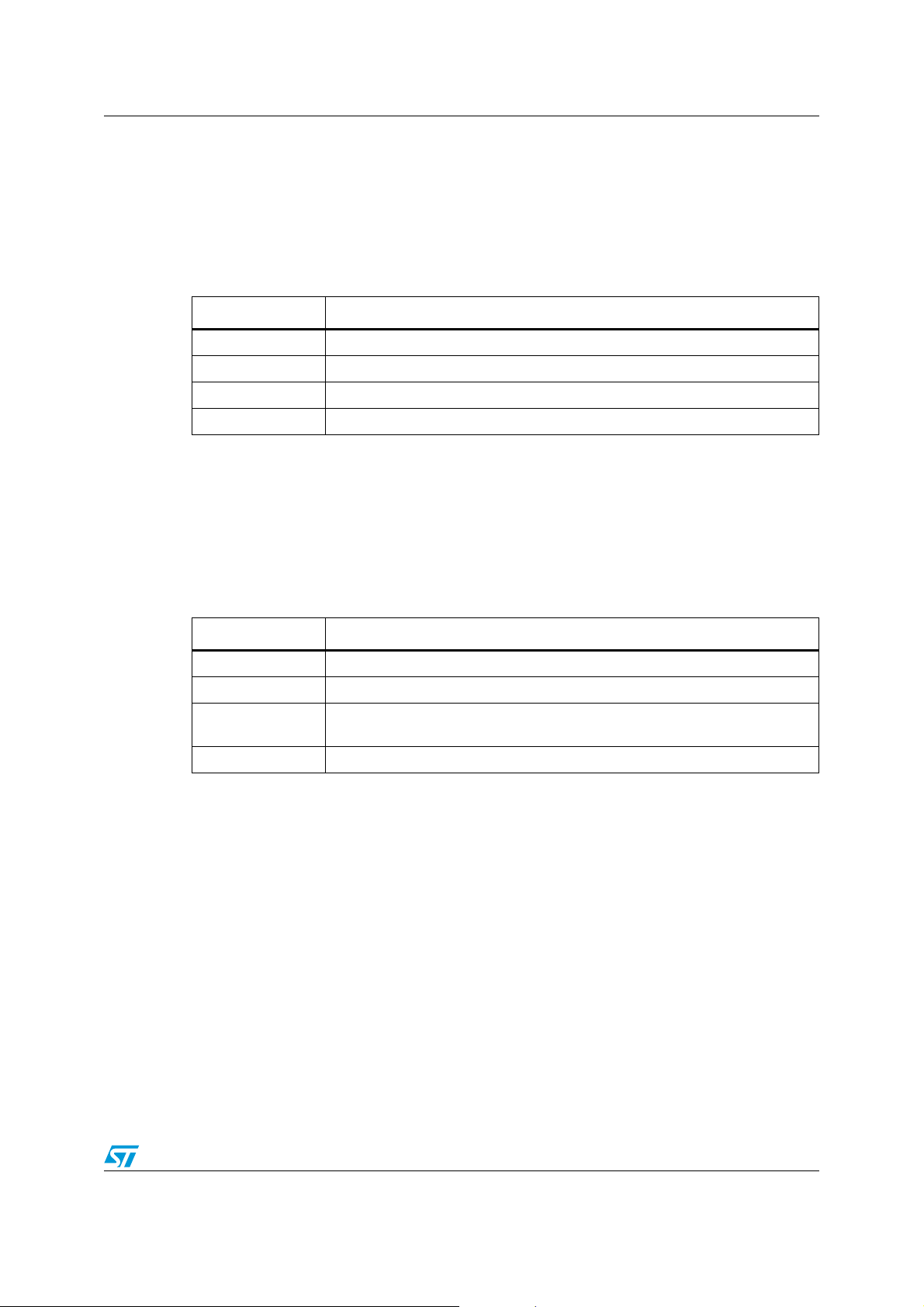
Table 7. Serial interface pin description
Pin name Pin description
SCL_A I
SDA_A I
SCL_M I
SDA_M I
7.1 I2C serial interface
The LSM303DLM I2C is a bus slave. The I2C is employed to write the data into the registers
whose content can also be read back.
The relevant I
2
2
C serial clock (SCL) for accelerometer
2
C serial data (SDA) for accelerometer
2
C serial clock (SCL) for magnetometer
2
C serial data (SDA) for magnetometer
C terminology is given in the table below.
Table 8. Serial interface pin description
Term Description
Transmitter The device which sends data to the bus
Receiver The device which receives data from the bus
Master
Slave The device addressed by the master
There are two signals associated with the I
The device which initiates a transfer, generates clock signals, and terminates a
transfer
2
C bus; the serial clock line (SCL) and the serial
data line (SDA). The latter is a bidirectional line used for sending and receiving the data
to/from the interface.
Doc ID 018725 Rev 1 17/38
Page 18
Digital interfaces LSM303DLM
7.1.1 I2C operation
The transaction on the bus is started through a START (ST) signal. A START condition is
defined as a HIGH to LOW transition on the data line while the SCL line is held HIGH. After
this has been transmitted by the master, the bus is considered busy. The next byte of data
transmitted after the start condition contains the address of the slave in the first 7 bits and
th
the 8
bit tells whether the master is receiving data from the slave or transmitting data to the
slave. When an address is sent, each device in the system compares the first seven bits
after a start condition with its address. If they match, the device considers itself addressed
by the master.
Data transfer with acknowledge is mandatory. The transmitter must release the SDA line
during the acknowledge pulse. The receiver must then pull the data line LOW so that it
remains stable low during the HIGH period of the acknowledge clock pulse. A receiver which
has been addressed is obliged to generate an acknowledge after each byte of data
received.
2
The I
C embedded inside the LSM303DLM behaves like a slave device and the following
protocol must be adhered to. After the start condition (ST) a slave address is sent. Once a
slave acknowledge (SAK) has been returned, an 8-bit sub-address (SUB) is transmitted; the
7 LSBs represent the actual register address while the MSB enables address autoincrement. If the MSb of the SUB field is ‘1’, the SUB (register address) is automatically
increased to allow multiple data read/write.
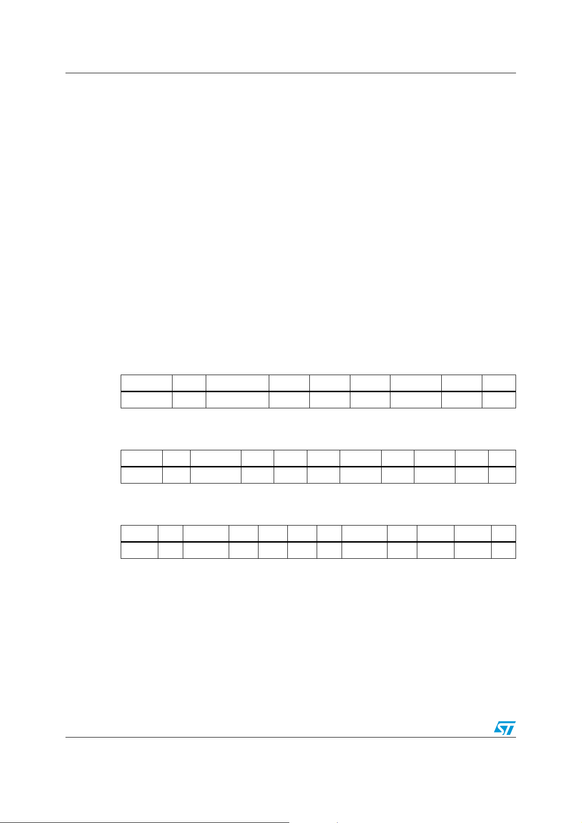
Table 9. Transfer when master is writing one byte to slave
Master ST SAD + W SUB DATA SP
Slave SAK SAK SAK
Table 10. Transfer when master is writing multiple bytes to slave
Master ST SAD + W SUB DATA DATA SP
Slave SAK SAK SAK SAK
Table 11. Transfer when master is receiving (reading) one byte of data from slave
Master ST SAD + W SUB SR SAD + R NMAK SP
Slave SAK SAK SAK DATA
Data are transmitted in byte format (DATA). Each data transfer contains 8 bits. The number
of bytes transferred per transfer is unlimited. Data is transferred with the most significant bit
(MSb) first. If a receiver cannot receive another complete byte of data until it has performed
some other function, it can hold the clock line SCL LOW to force the transmitter into a wait
state. Data transfer only continues when the receiver is ready for another byte and releases
the data line. If a slave receiver does not acknowledge the slave address (i.e. it is not able to
receive because it is performing a real-time function) the data line must be left HIGH by the
slave. The master can then abort the transfer. A LOW to HIGH transition on the SDA line
while the SCL line is HIGH is defined as a STOP condition. Each data transfer must be
terminated by the generation of a STOP (SP) condition.
18/38 Doc ID 018725 Rev 1
Page 19
LSM303DLM Digital interfaces
7.1.2 Linear acceleration digital interface
For linear acceleration, the default (factory) 7-bit slave address is 001100xb. The SDO/SA0
pad can be used to modify the least significant bit of the device address. If the SA0 pad is
connected to voltage supply, the LSB is ‘1’ (address 0011001b) otherwise, if the SA0 pad is
connected to ground, the LSB value is ‘0’ (address 0011000b). This solution permits
connecting and addressing two different accelerometers to the same I
The slave address is completed with a read/write bit. If the bit is ‘1’ (read), a repeated
START (SR) condition must be issued after the two sub-address bytes; if the bit is ‘0’ (write),
the master transmits to the slave with the direction unchanged. Table 12 explains how the
SAD+read/write bit pattern is composed, listing all the possible configurations.
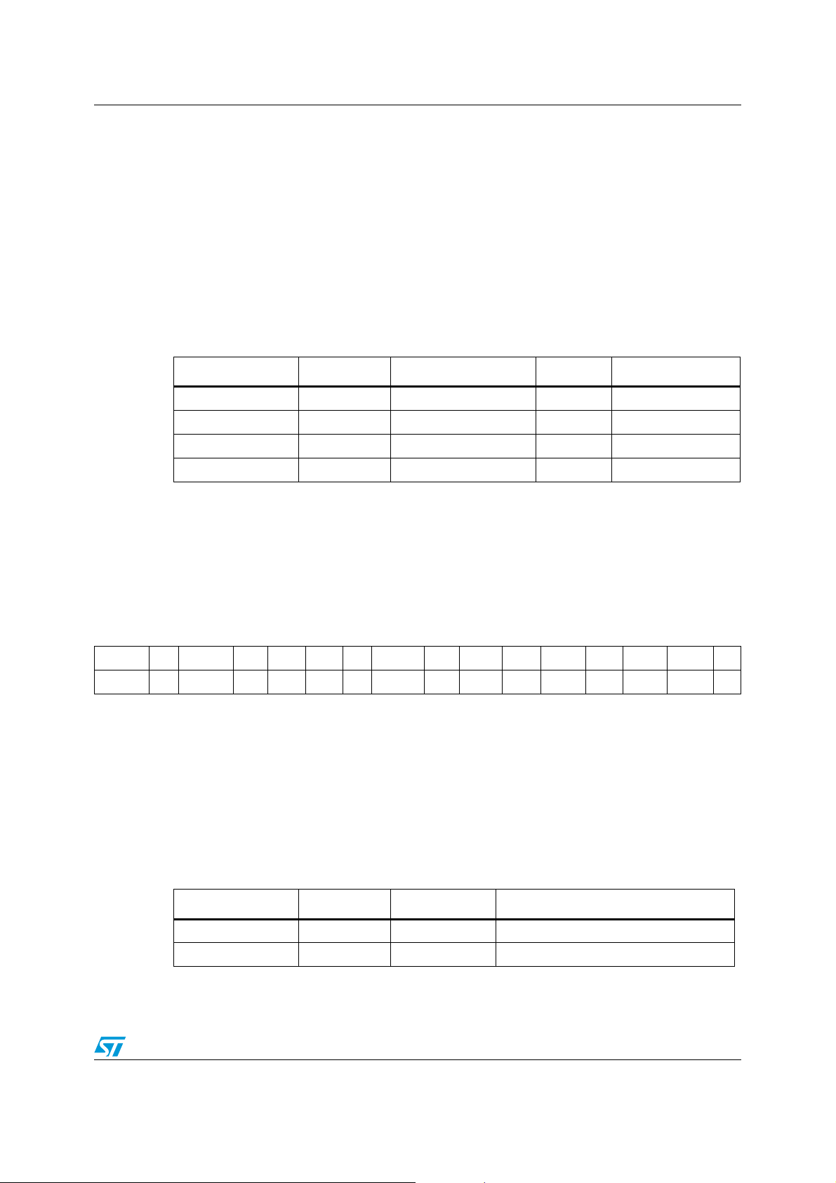
Table 12. SAD and read/write patterns
Command SAD[6:1] SAD[0] = SA0 R/W SAD+R/W
Read 001100 0 1 00110001 (31h)
Write 001100 0 0 00110000 (30h)
Read 001100 1 1 00110011 (33h)
Write 001100 1 0 00110010 (32h)
2
C lines.
In order to read multiple bytes, it is necessary to assert the most significant bit of the subaddress field. In other words, SUB(7) must be equal to 1 while SUB(6-0) represents the
address of the first register to be read.
In the presented communication format, MAK is master acknowledge and NMAK is no
master acknowledge.
Table 13. Transfer when master is receiving (reading) multiple bytes of data from slave
Master ST SAD+W SUB SR SAD+R MAK MAK NMAK SP
Slave SAK SAK SAK DATA DATA DATA
7.1.3 Magnetic field digital interface
For magnetic sensors the default (factory) 7-bit slave address is 0011110xb.
The slave address is completed with a read/write bit. If the bit is ‘1’ (read), a repeated
START (SR) condition must be issued after the two sub-address bytes; if the bit is ‘0’ (write),
the master transmits to the slave with the direction unchanged. Table 14 explains how the
SAD is composed.
Table 14. SAD and read/write patterns
Command SAD[6:0] R/W SAD+R/W
Read 0011110 1 00111101 (3Dh)
Write 0011110 0 00111100 (3Ch)
Doc ID 018725 Rev 1 19/38
Page 20

Digital interfaces LSM303DLM
Magnetic signal interface reading/writing
The interface uses an address pointer to indicate which register location is to be read from
or written to. These pointer locations are sent from the master to this slave device and
succeed the 7-bit address plus 1 bit read/write identifier.
To minimize communication between the master and magnetic digital interface of
LSM303DLM, the address pointer updates automatically without master intervention.
This automatic address pointer update has two additional features. First, when address 12
or higher is accessed, the pointer updates to address 00, and secondly, when address 08 is
reached, the pointer rolls back to address 03. Logically, the address pointer operation
functions as shown below.
If (address pointer = 08) then the address pointer = 03
Or else, if (address pointer >= 12) then the address pointer = 0
Or else, (address pointer) = (address pointer) + 1
The address pointer value itself cannot be read via the I
Any attempt to read an invalid address location returns 0, and any write to an invalid
address location, or an undefined bit within a valid address location, is ignored by this
device.
2
C bus.
20/38 Doc ID 018725 Rev 1
Page 21
LSM303DLM Register mapping
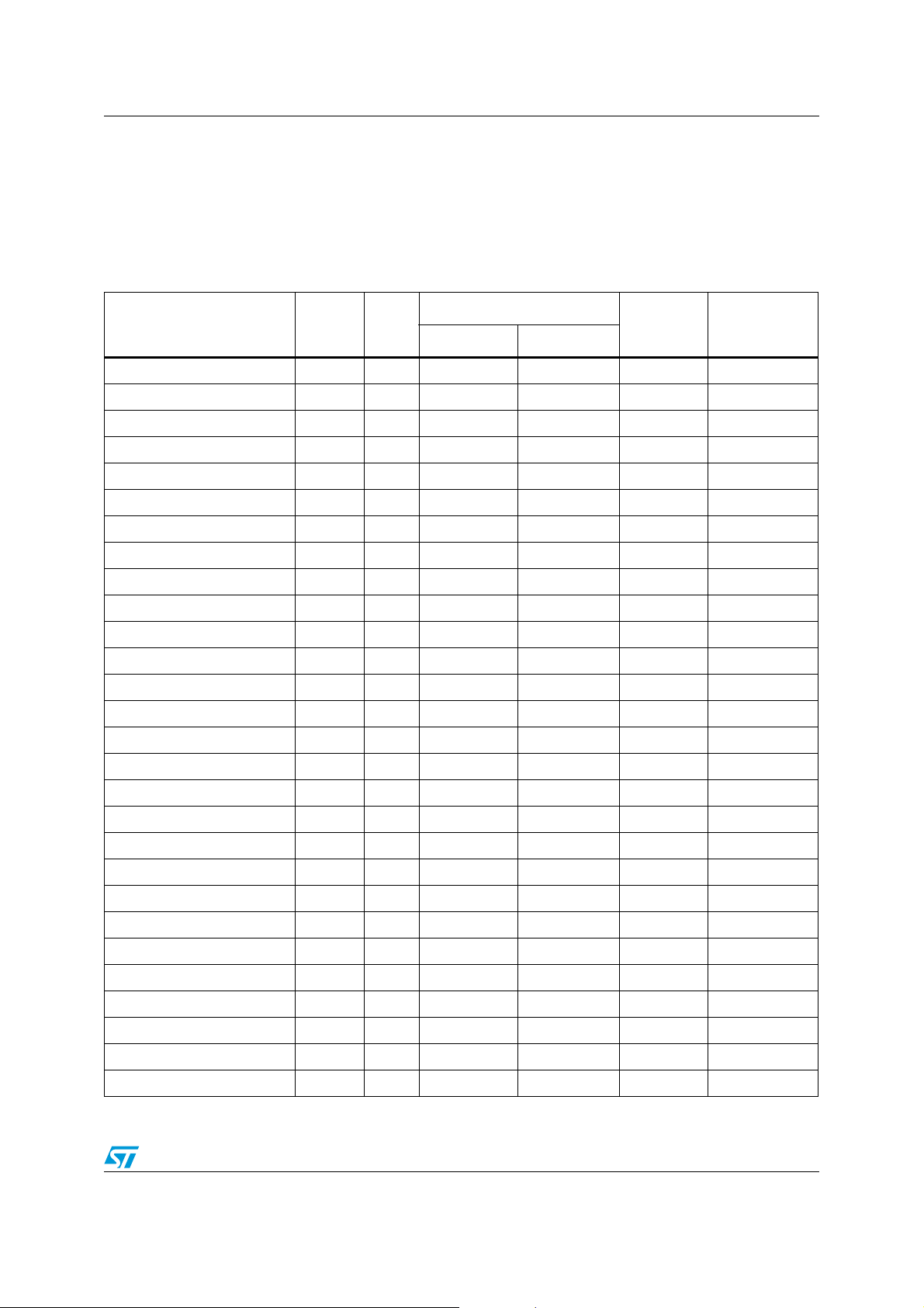
8 Register mapping
Table 15 provides a listing of the 8-bit registers embedded in the device and the related
addresses:
Table 15. Register address map
Name
Reserved (do not modify) Table 12 -- 00 - 1F -- -- Reserved
CTRL_REG1_A Table 12 rw 20 010 0000 00000111
CTRL_REG2_A Table 12 rw 21 010 0001 00000000
CTRL_REG3_A Table 12 rw 22 010 0010 00000000
CTRL_REG4_A Table 12 rw 23 010 0011 00000000
CTRL_REG5_A Table 12 rw 24 010 0100 00000000
HP_FILTER_RESET_A Table 12 r 25 010 0101 -- Dummy register
REFERENCE_A Table 12 rw 26 010 0110 00000000
STATUS_REG_A Table 12 r 27 010 0111 00000000
OUT_X_L_A Table 12 r 28 010 1000 output
OUT_X_H_A Table 12 r 29 010 1001 output
OUT_Y_L_A Table 12 r 2A 010 1010 output
OUT_Y_H_A Table 12 r 2B 010 1011 output
OUT_Z_L_A Table 12 r 2C 010 1100 output
OUT_Z_H_A Table 12 r 2D 010 1101 output
Reserved (do not modify) Table 12 -- 2E - 2F -- -- Reserved
Slave
address
Type
Register address
Default Comment
Hex Binary
INT1_CFG_A Table 12 rw 30 011 0000 00000000
INT1_SOURCE_A Table 12 r 31 011 0001 00000000
INT1_THS_A Table 12 rw 32 011 0010 00000000
INT1_DURATION_A Table 12 rw 33 011 0011 00000000
INT2_CFG_A Table 12 rw 34 011 0100 00000000
INT2_SOURCE_A Table 12 r 35 011 0101 00000000
INT2_THS_A Table 12 rw 36 011 0110 00000000
INT2_DURATION_A Table 12 rw 37 011 0111 00000000
Reserved (do not modify) Table 12 -- 38 - 3F -- -- Reserved
CRA_REG_M Table 14 rw 00 00000000 00010000
CRB_REG_M Table 14 rw 01 00000001 00100000
MR_REG_M Table 14 rw 02 00000010 00000011
Doc ID 018725 Rev 1 21/38
Page 22
Register mapping LSM303DLM
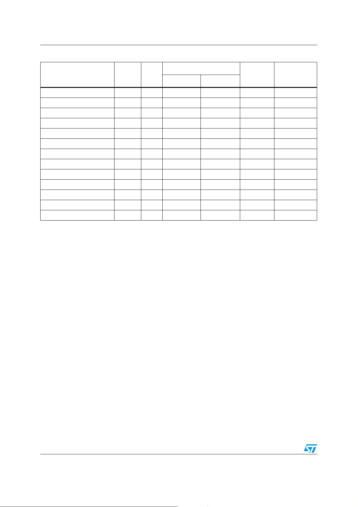
Table 15. Register address map (continued)
Name
OUT_X_H_M Table 14 r 03 00000011 output
OUT_X_L_M Table 14 r 04 00000100 output
OUT_Y_H_M Table 14 r 07 00000101 output
OUT_Y_L_M Table 14 r 08 00000110 output
OUT_Z_H_M Table 14 r 05 00000111 output
OUT_Z_L_M Table 14 r 06 00001000 output
SR_REG_Mg Table 14 r 09 00001001 00000000
IRA_REG_M Table 14 r 0A 00001010 01001000
IRB_REG_M Table 14 r 0B 00001011 00110100
IRC_REG_M Table 14 r 0C 00001100 00110011
Reserved (do not modify) Table 14 -- 0D - 0E -- -- Reserved
WHO_AM_I_M Table 14 r 0F 00001111 00111100 Who am I ID
Reserved (do not modify) Table 14 -- 10 - 3A -- -- Reserved
Slave
address
Type
Register address
Default Comment
Hex Binary
Registers marked as “reserved” must not be changed. Writing to these registers may cause
permanent damage to the device.
The content of the registers that are loaded at boot should not be changed. They contain the
factory calibrated values. Their content is automatically restored when the device is powered
up.
22/38 Doc ID 018725 Rev 1
Page 23
LSM303DLM Register description
9 Register description
The device contains a set of registers which are used to control its behavior and to retrieve
acceleration data. The register address, made up of 7 bits, is used to identify them and to
write the data through the serial interface.
9.1 Linear acceleration register description
9.1.1 CTRL_REG1_A (20h)
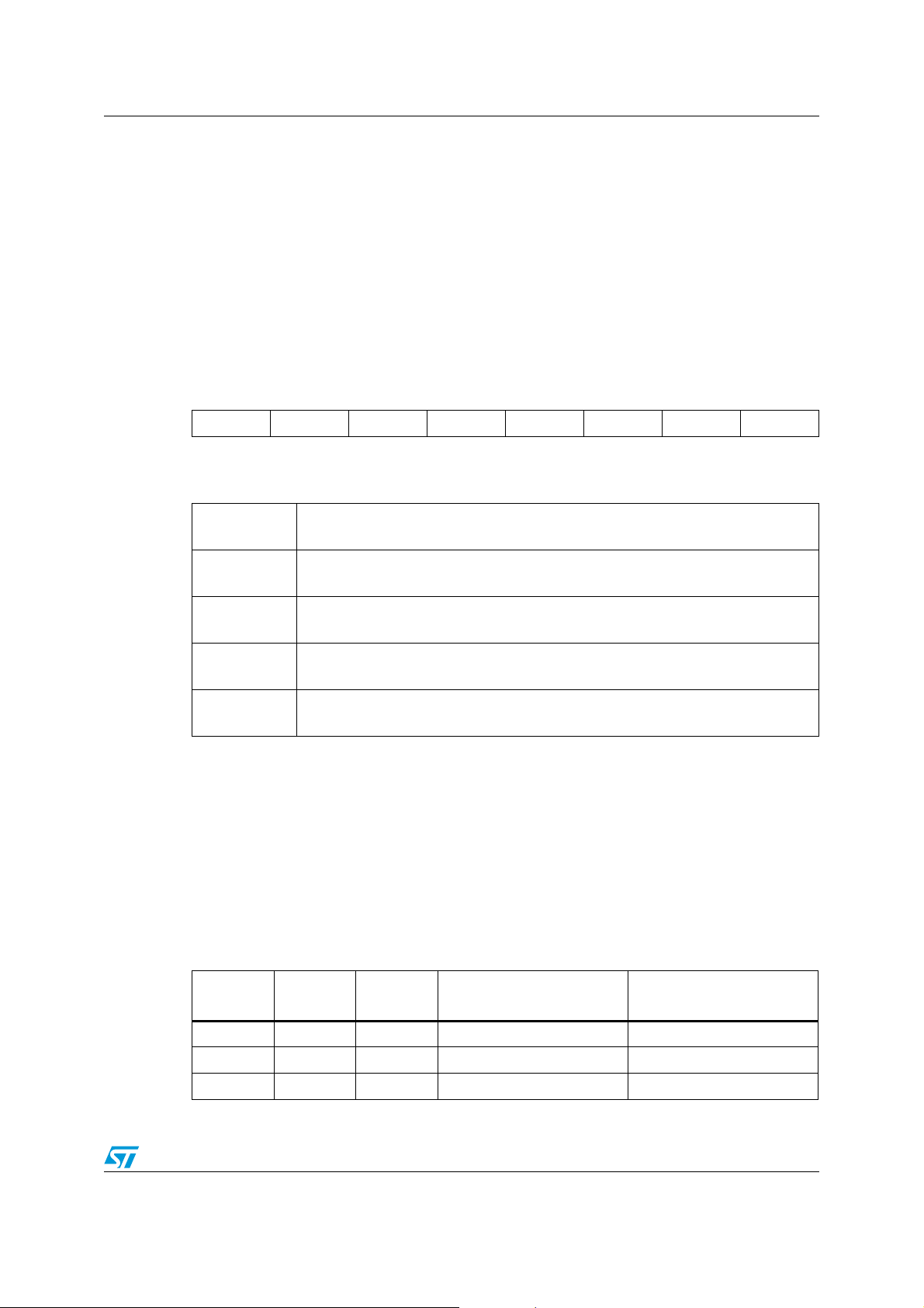
Table 16. CTRL_REG1_A register
PM2 PM1 PM0 DR1 DR0 Zen Yen Xen
Table 17. CTRL_REG1_A description
PM2 - PM0
DR1, DR0
Zen
Ye n
Xen
Power mode selection. Default value: 000
(000: power-down; others: refer to Table 18)
Data rate selection. Default value: 00
(00:50 Hz; others: refer to Table 19)
Z axis enable. Default value: 1
(0: Z axis disabled; 1: Z axis enabled)
Y axis enable. Default value: 1
(0: Y axis disabled; 1: Y axis enabled)
X axis enable. Default value: 1
(0: X axis disabled; 1: X axis enabled)
PM bits allow selection between power-down and two operating active modes. The device is
in power-down mode when the PD bits are set to “000” (default value after boot).
Table 18
shows all the possible power mode configurations and respective output data rates. Output
data in the low-power modes are computed with a low-pass filter cut-off frequency defined
by DR1 and DR0 bits.
DR bits, in normal-mode operation, select the data rate at which acceleration samples are
produced. In low-power mode they define the output data resolution.
Table 19 shows all the
possible configurations for the DR1 and DR0 bits.
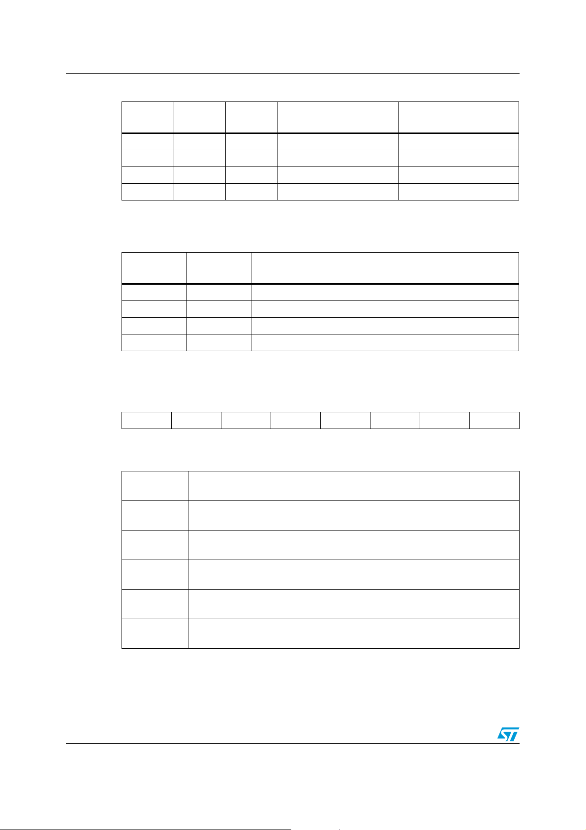
Table 18. Power mode and low-power output data rate configurations
PM2 PM1 PM0 Power mode selection
0 0 0 Power-down --
0 0 1 Normal mode ODR
0 1 0 Low-power 0.5
Doc ID 018725 Rev 1 23/38
Output data rate [Hz]
ODR
LP
Page 24
Register description LSM303DLM
Table 18. Power mode and low-power output data rate configurations (continued)
PM2 PM1 PM0 Power mode selection
0 1 1 Low-power 1
1 0 0 Low-power 2
1 0 1 Low-power 5
1 1 0 Low-power 10
Table 19. Normal-mode output data rate configurations and low-pass cut-off
frequencies
DR1 DR0
00 50 37
01 100 74
1 0 400 292
1 1 1000 780
9.1.2 CTRL_REG2_A (21h)
Output data rate [Hz]
ODR
Output data rate [Hz]
ODR
LP
Low-pass filter cut-off
frequency [Hz]
Table 20. CTRL_REG2_A register
BOOT HPM1 HPM0 FDS HPen2 HPen1 HPCF1 HPCF0
Table 21. CTRL_REG2_A description
BOOT
HPM1, HPM0
FDS
HPen2
HPen1
HPCF1,
HPCF0
Reboot memory content. Default value: 0
(0: normal mode; 1: reboot memory content)
High-pass filter mode selection. Default value: 00
(00: normal mode; others: refer to Table 22)
Filtered data selection. Default value: 0
(0: internal filter bypassed; 1: data from internal filter sent to output register)
High-pass filter enabled for Interrupt 2 source. Default value: 0
(0: filter bypassed; 1: filter enabled)
High-pass filter enabled for Interrupt 1 source. Default value: 0
(0: filter bypassed; 1: filter enabled)
High-pass filter cut-off frequency configuration. Default value: 00
(00: HPc=8; 01: HPc=16; 10: HPc=32; 11: HPc=64)
The BOOT bit is used to refresh the content of internal registers stored in the Flash memory
block. At device power-up, the content of the Flash memory block is transferred to the
internal registers related to trimming functions to permit good device behavior. If, for any
24/38 Doc ID 018725 Rev 1
Page 25
LSM303DLM Register description
reason, the content of the trimming registers has changed, it is sufficient to use this bit to
restore the correct values. When the BOOT bit is set to ‘1’ the content of the internal Flash is
copied to the corresponding internal registers and is used to calibrate the device. These
values are factory-trimmed and are different for every accelerometer. They permit good
device behavior and normally do not have to be modified. At the end of the boot process, the
BOOT bit is again set to ‘0’.
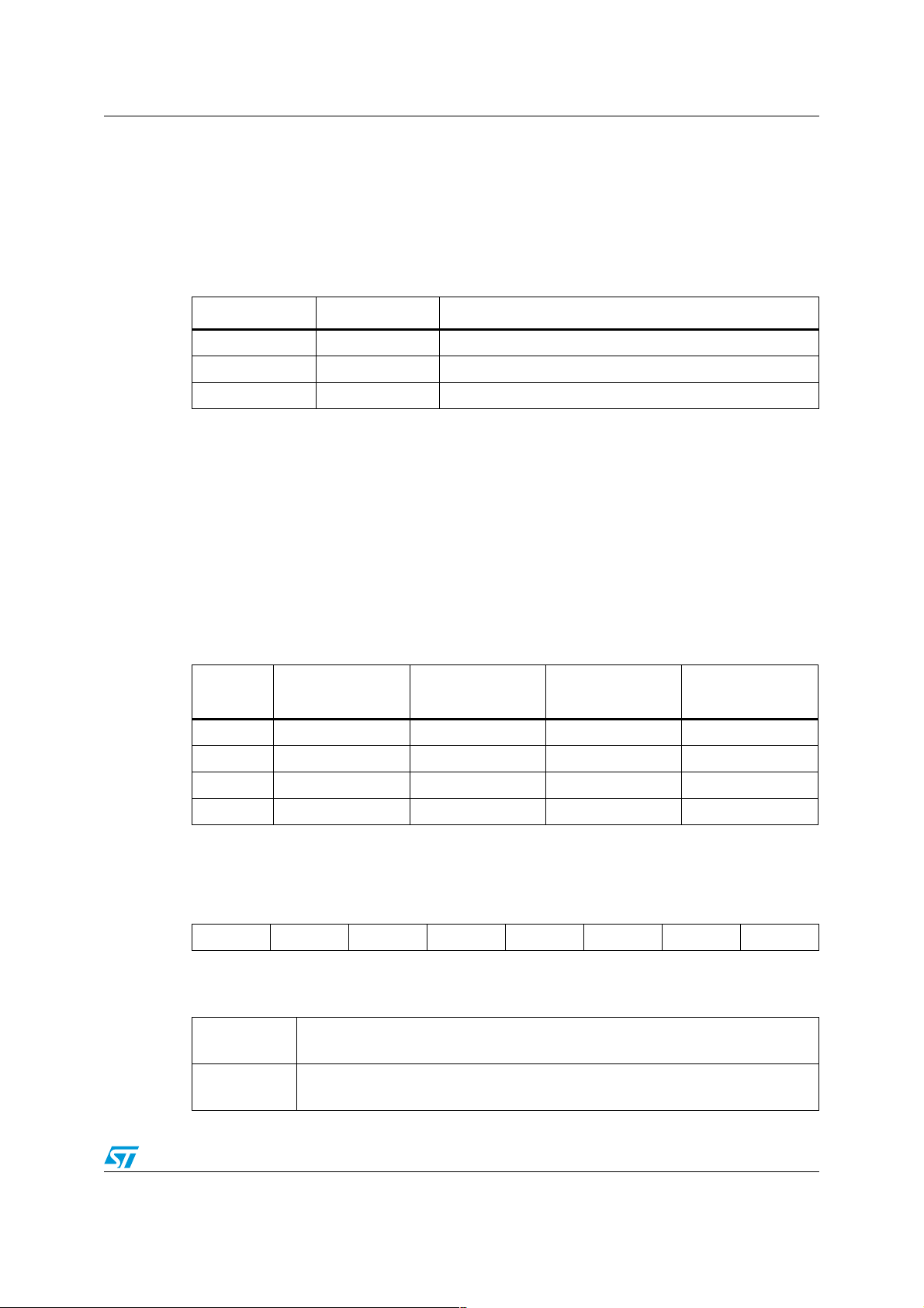
Table 22. High-pass filter mode configuration
HPM1 HPM0 High-pass filter mode
0 0 Normal mode (reset reading HP_RESET_FILTER)
0 1 Reference signal for filtering
1 0 Normal mode (reset reading HP_RESET_FILTER)
HPCF[1:0]. These bits are used to configure the high-pass filter cut-off frequency (f
is given by:
The equation can be simplified to the following approximated equation:
Table 23. High-pass filter cut-off frequency configuration
[Hz]
f
HPcoeff2,1
t
Data rate = 50 Hz
00 1 2 8 20
01 0.5 1 4 10
10 0.25 0.5 2 5
11 0.125 0.25 1 2.5
9.1.3 CTRL_REG3_A (22h)
f
1
t
⎝⎠
----------------------=
f
t
6HPc⋅
----------- -–
HPc
f
s
1
⎛⎞
ft [Hz]
Data rate = 100 Hz
f
s
------
⋅ln=
2π
ft [Hz]
Data rate = 400 Hz
, which
t)
ft [Hz]
Data rate = 1000 Hz
Table 24. CTRL_REG3_A register
IHL PP_OD LIR2 I2_CFG1 I2_CFG0 LIR1 I1_CFG1 I1_CFG0
Table 25. CTRL_REG3_A description
IHL
PP_OD
Interrupt active high, low. Default value: 0
(0: active high; 1: active low)
Push-pull/open drain selection on interrupt pad. Default value 0.
(0: push-pull; 1: open drain)
Doc ID 018725 Rev 1 25/38
Page 26
Register description LSM303DLM
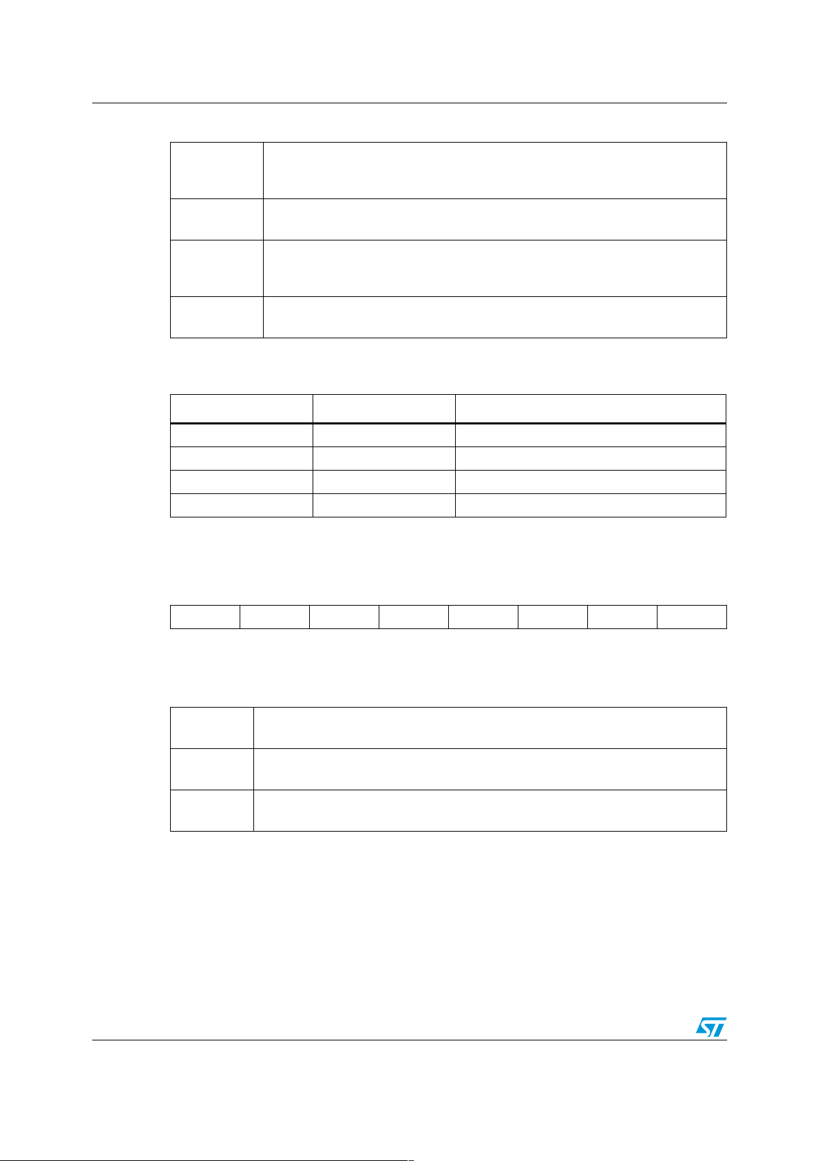
Table 25. CTRL_REG3_A description (continued)
Latch interrupt request on INT2_SRC register, with INT2_SRC register cleared by
LIR2
reading INT2_SRC itself. Default value: 0.
(0: interrupt request not latched; 1: interrupt request latched)
I2_CFG1,
I2_CFG0
LIR1
I1_CFG1,
I1_CFG0
Data signal on INT 2 pad control bits. Default value: 00.
(see Table 26)
Latch interrupt request on INT1_SRC register, with INT1_SRC register cleared by
reading INT1_SRC register. Default value: 0.
(0: interrupt request not latched; 1: interrupt request latched)
Data signal on INT 1 pad control bits. Default value: 00.
(see Table 26)
Table 26. Data signal on INT 1 and INT 2 pad
I1(2)_CFG1 I1(2)_CFG0 INT 1(2) Pad
0 0 Interrupt 1 (2) source
0 1 Interrupt 1 source OR Interrupt 2 source
1 0 Data ready
1 1 Boot running
9.1.4 CTRL_REG4_A (23h)
Table 27. CTRL_REG4_A register
BDU BLE FS1 FS0 0 0 0
1. This bit must be set to ‘0’ for correct working of the device.
(1)
---
Table 28. CTRL_REG4_A description
BDU
BLE
FS1, FS0
Block data update. Default value: 0
(0: continuos update; 1: output registers not updated between MSB and LSB reading)
Big/little endian data selection. Default value 0.
(0: data LSB @ lower address; 1: data MSB @ lower address)
Full-scale selection. Default value: 00.
(00: ±2 g; 01: ±4 g; 11: ±8 g)
The BDU bit is used to inhibit output register updates between the reading of the upper and
lower register parts. In default mode (BDU = ‘0’), the lower and upper register parts are
updated continuously. If it is not certain whether to read faster than the output data rate, it is
recommended to set BDU bit to ‘1’. In this way, after the reading of the lower (upper) register
part, the content of that output register is not updated until the upper (lower) part is read
also. This feature avoids reading LSB and MSB related to different samples.
26/38 Doc ID 018725 Rev 1
Page 27
LSM303DLM Register description
9.1.5 CTRL_REG5_A (24h)
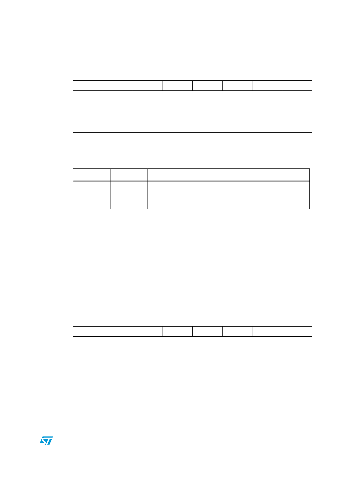
Table 29. CTRL_REG5_A register
000000TurnOn1TurnOn0
Table 30. CTRL_REG5_A description
Tu r n On 1 ,
Tu r n On 0
Turn O n bits are used for turning on the sleep-to-wakeup function.
Table 31. Sleep-to-wakeup configuration
TurnOn1 TurnOn0 Sleep-to-wakeup status
0 0 Sleep-to-wakeup function is disabled
11
Turn-on mode selection for sleep-to-wakeup function. Default value: 00.
Turned on: the device is in low-power mode
(ODR is defined in CTRL_REG1_A)
By setting the TurnOn [1:0] bits to 11, the “sleep-to-wakeup” function is enabled. When an
interrupt event occurs, the device goes into normal mode, increasing the ODR to the value
defined in CTRL_REG1_A. Although the device is in normal mode, CTRL_REG1_A content
is not automatically changed to “normal mode” configuration.
9.1.6 HP_FILTER_RESET_A (25h)
Dummy register. Reading at this address instantaneously zeroes the content of the internal
high-pass filter. If the high-pass filter is enabled, all three axes are instantaneously set to 0
g. This makes it possible to surmount the settling time of the high-pass filter.
9.1.7 REFERENCE_A (26h)
Table 32. REFERENCE_A register
Ref7 Ref6 Ref5 Ref4 Ref3 Ref2 Ref1 Ref0
Table 33. REFERENCE_A description
Ref7 - Ref0 Reference value for high-pass filter. Default value: 00h.
This register sets the acceleration value taken as a reference for the high-pass filter output.
When the filter is turned on (at least one FDS, HPen2, or HPen1 bit is equal to ‘1’) and HPM
bits are set to “01”, filter out is generated taking this value as a reference.
Doc ID 018725 Rev 1 27/38
Page 28
Register description LSM303DLM
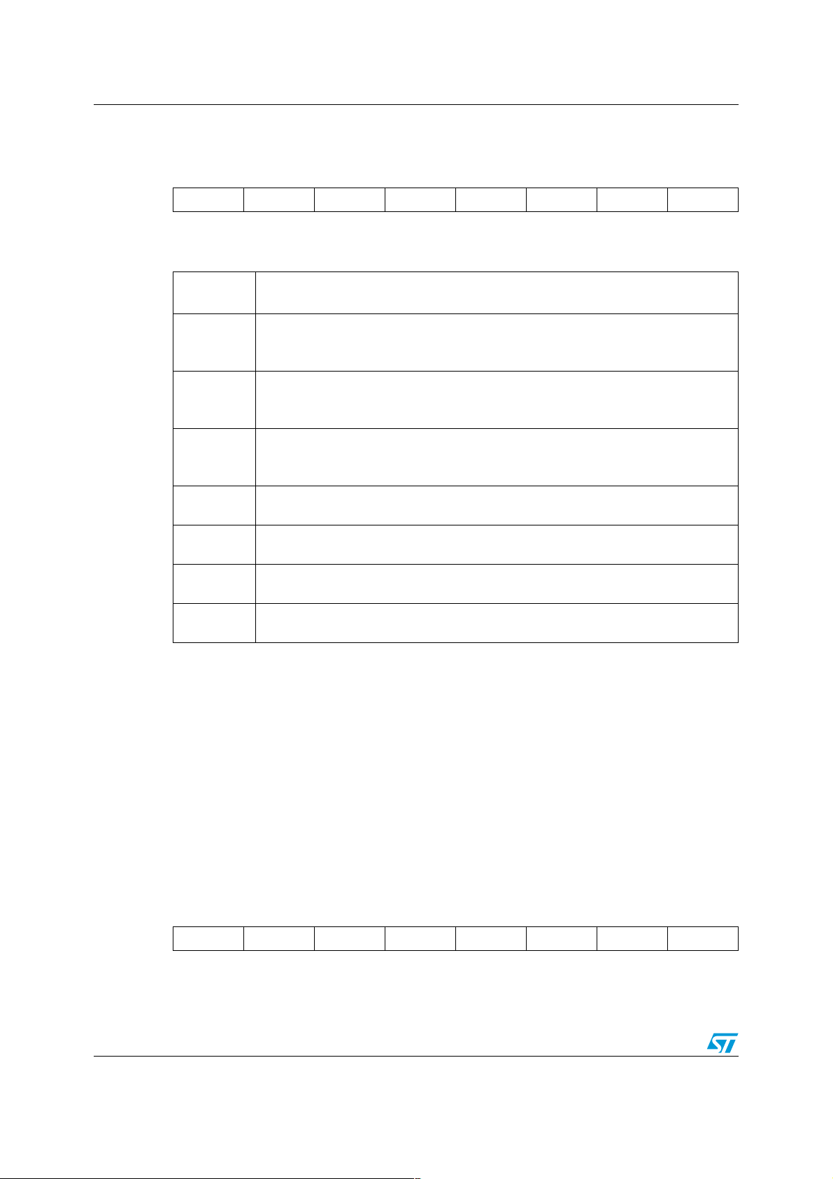
9.1.8 STATUS_REG_A(27h)
Table 34. STATUS_REG_A register
ZYXOR ZOR YOR XOR ZYXDA ZDA YDA XDA
Table 35. STATUS_REG_A description
ZYXOR
ZOR
YOR
XOR
ZYXDA X, Y, and Z axis new data available. Default value: 0
ZDA Z axis new data available. Default value: 0
X, Y, and Z axis data overrun. Default value: 0
(0: no overrun has occurred, 1: new data has overwritten the previous one)
Z axis data overrun. Default value: 0
(0: no overrun has occurred, 1: new data for the Z-axis has overwritten the previous
one)
Y axis data overrun. Default value: 0
(0: no overrun has occurred, 1: new data for the Y-axis has overwritten the previous
one)
X axis data overrun. Default value: 0
(0: no overrun has occurred, 1: new data for the X-axis has overwritten the previous
one)
(0: a new set of data is not yet available, 1: a new set of data is available)
(0: new data for the Z-axis is not yet available, 1: new data for the Z-axis is available)
YDA Y axis new data available. Default value: 0
(0: new data for the Y-axis is not yet available, 1: new data for the Y-axis is available)
XDA X axis new data available. Default value: 0
(0: new data for the X-axis is not yet available, 1: new data for the X-axis is available)
9.1.9 OUT_X_L_A (28h), OUT_X_H_A (29h)
X-axis acceleration data. The value is expressed as 2’s complement.
9.1.10 OUT_Y_L_A (2Ah), OUT_Y_H_A (2Bh)
Y-axis acceleration data. The value is expressed as 2’s complement.
9.1.11 OUT_Z_L_A (2Ch), OUT_Z_H_A (2Dh)
Z-axis acceleration data. The value is expressed as 2’s complement.
9.1.12 INT1_CFG_A (30h)
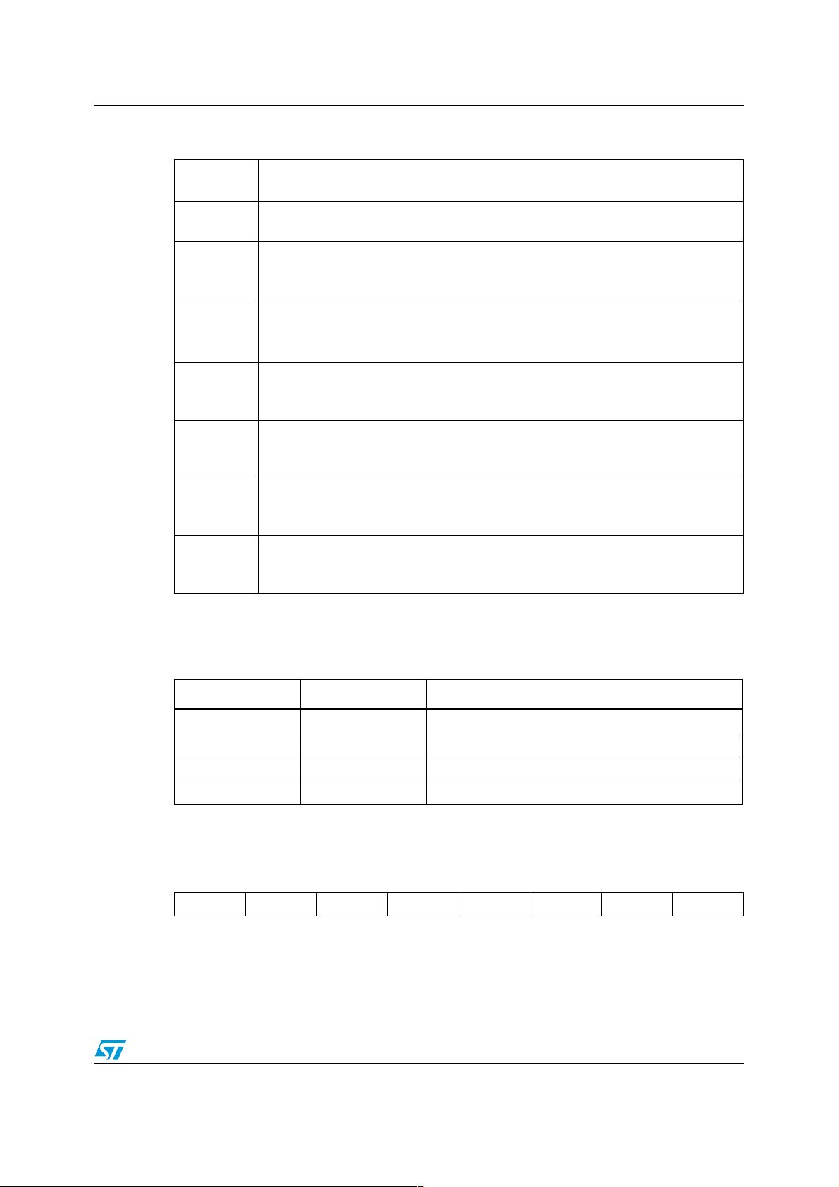
Table 36. INT1_CFG_A register
AOI 6D ZHIE ZLIE YHIE YLIE XHIE XLIE
28/38 Doc ID 018725 Rev 1
Page 29
LSM303DLM Register description
Table 37. INT1_CFG_A description
AOI
6D
ZHIE
ZLIE
YHIE
YLIE
XHIE
XLIE
AND/OR combination of interrupt events. Default value: 0
(see Table 38).
6-direction detection function enable. Default value: 0
(see Table 38).
Enable interrupt generation on Z high event. Default value: 0
(0: disable interrupt request,
1: enable interrupt request on measured accel. value higher than preset threshold)
Enable interrupt generation on Z low event. Default value: 0
(0: disable interrupt request,
1: enable interrupt request on measured accel. value lower than preset threshold)
Enable interrupt generation on Y high event. Default value: 0
(0: disable interrupt request,
1: enable interrupt request on measured accel. value higher than preset threshold)
Enable interrupt generation on Y low event. Default value: 0
(0: disable interrupt request,
1: enable interrupt request on measured accel. value lower than preset threshold)
Enable interrupt generation on X high event. Default value: 0
(0: disable interrupt request,
1: enable interrupt request on measured accel. value higher than preset threshold)
Enable interrupt generation on X low event. Default value: 0
(0: disable interrupt request,
1: enable interrupt request on measured accel. value lower than preset threshold)
Configuration register for Interrupt 1 source.
Table 38. Interrupt 1 source configurations
AOI 6D Interrupt mode
0 0 OR combination of interrupt events
0 1 6-direction movement recognition
1 0 AND combination of interrupt events
1 1 6-direction position recognition
9.1.13 INT1_SRC_A (31h)
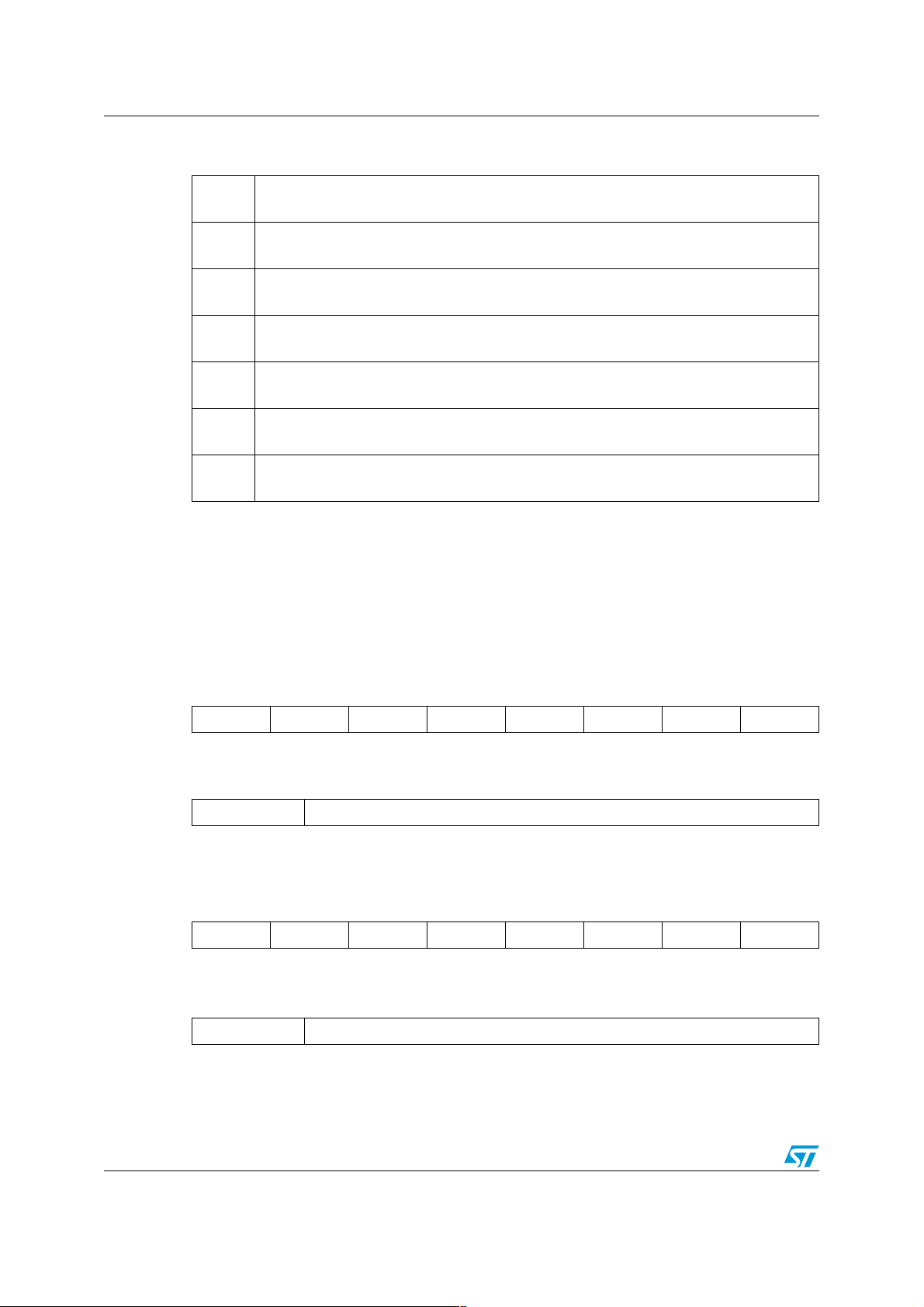
Table 39. INT1_SRC register
0 IA ZHZLYHYLXHXL
Doc ID 018725 Rev 1 29/38
Page 30
Register description LSM303DLM
Table 40. INT1_SRC_A description
IA
ZH
ZL
YH
YL
XH
XL
Interrupt active. Default value: 0
(0: no interrupt has been generated, 1: one or more interrupts have been generated)
Z high. Default value: 0
(0: no interrupt, 1: Z high event has occurred)
Z low. Default value: 0
(0: no interrupt, 1: Z low event has occurred)
Y high. Default value: 0
(0: no interrupt, 1: Y high event has occurred)
Y low. Default value: 0
(0: no interrupt, 1: Y low event has occurred)
X high. Default value: 0
(0: no interrupt, 1: X high event has occurred)
X low. Default value: 0
(0: no interrupt, 1: X low event has occurred)
Interrupt 1 source register. Read-only register.
Reading at this address clears the INT1_SRC_A IA bit (and the interrupt signal on the INT 1
pin) and allows the refreshing of data in the INT1_SRC_A register if the latched option was
chosen.
9.1.14 INT1_THS_A (32h)
Table 41. INT1_THS register
0 THS6 THS5 THS4 THS3 THS2 THS1 THS0
Table 42. INT1_THS description
THS6 - THS0 Interrupt 1 threshold. Default value: 000 0000
9.1.15 INT1_DURATION_A (33h)
Table 43. INT1_DURATION_A register
0 D6D5D4D3D2D1D0
Table 44. INT2_DURATION_A description
D6 - D0 Duration value. Default value: 000 0000
The D6 - D0 bits set the minimum duration of the Interrupt 2 event to be recognized.
Duration steps and maximum values depend on the ODR chosen.
30/38 Doc ID 018725 Rev 1
Page 31
LSM303DLM Register description
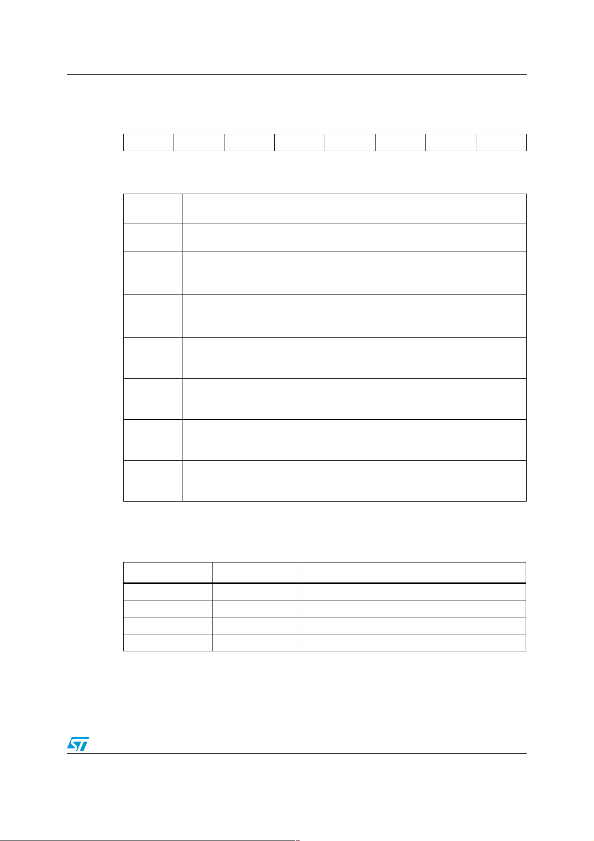
9.1.16 INT2_CFG_A (34h)
Table 45. INT2_CFG_A register
AOI 6D ZHIE ZLIE YHIE YLIE XHIE XLIE
Table 46. INT2_CFG_A description
AOI
6D
ZHIE
ZLIE
YHIE
AND/OR combination of interrupt events. Default value: 0
(see Table 47).
6-direction detection function enable. Default value: 0
(see Table 47).
Enable interrupt generation on Z high event. Default value: 0
(0: disable interrupt request,
1: enable interrupt request on measured accel. value higher than preset threshold)
Enable interrupt generation on Z low event. Default value: 0
(0: disable interrupt request,
1: enable interrupt request on measured accel. value lower than preset threshold)
Enable interrupt generation on Y high event. Default value: 0
(0: disable interrupt request,
1: enable interrupt request on measured accel. value higher than preset threshold)
Enable interrupt generation on Y low event. Default value: 0
YLIE
XHIE
XLIE
(0: disable interrupt request,
1: enable interrupt request on measured accel. value lower than preset threshold)
Enable interrupt generation on X high event. Default value: 0
(0: disable interrupt request,
1: enable interrupt request on measured accel. value higher than preset threshold)
Enable interrupt generation on X low event. Default value: 0
(0: disable interrupt request,
1: enable interrupt request on measured accel. value lower than preset threshold)
Configuration register for Interrupt 2 source.
Table 47. Interrupt mode configuration
AOI 6D Interrupt mode
0 0 OR combination of interrupt events
0 1 6-direction movement recognition
1 0 AND combination of interrupt events
1 1 6-direction position recognition
Doc ID 018725 Rev 1 31/38
Page 32
Register description LSM303DLM
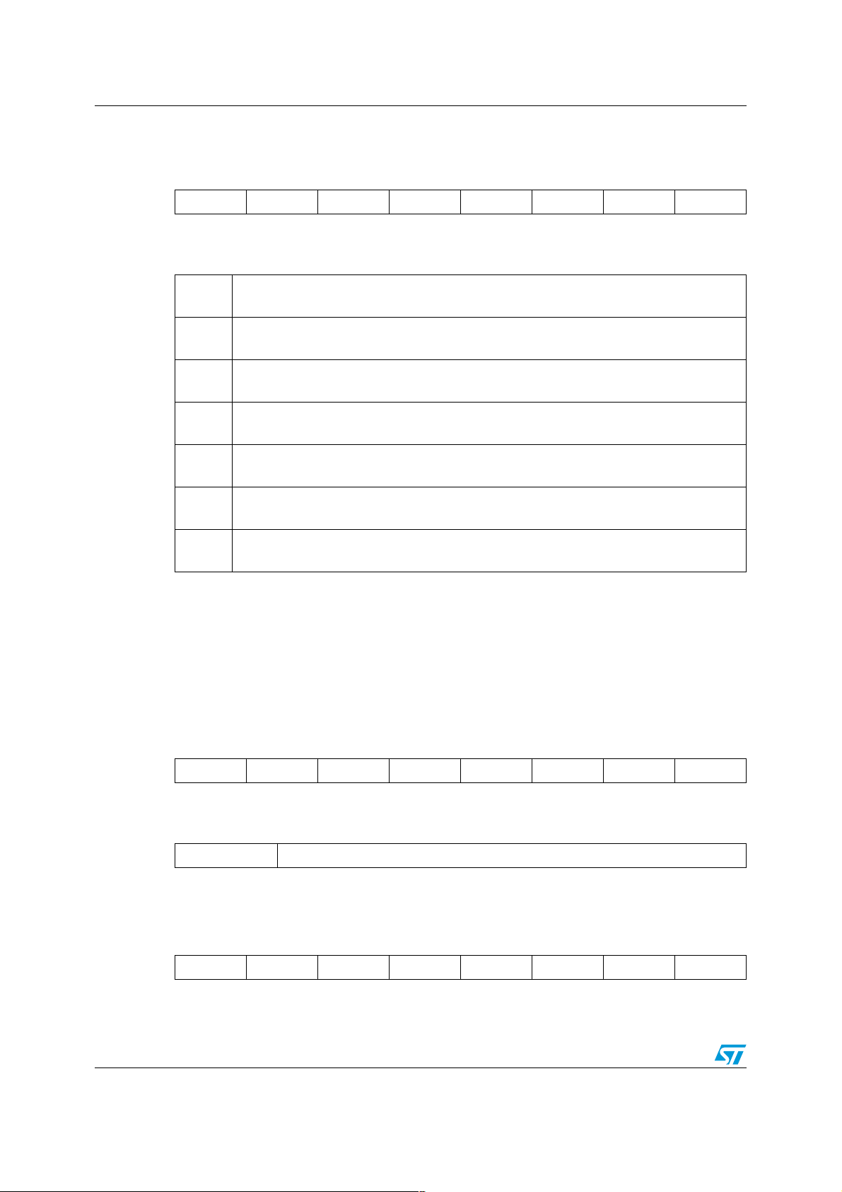
9.1.17 INT2_SRC_A (35h)
Table 48. INT2_SRC_A register
0 IA ZHZLYHYLXHXL
Table 49. INT2_SRC_A description
IA
ZH
ZL
YH
YL
XH
XL
Interrupt active. Default value: 0
(0: no interrupt has been generated; 1: one or more interrupts have been generated)
Z high. Default value: 0
(0: no interrupt, 1: Z high event has occurred)
Z low. Default value: 0
(0: no interrupt; 1: Z low event has occurred)
Y high. Default value: 0
(0: no interrupt, 1: Y high event has occurred)
Y low. Default value: 0
(0: no interrupt, 1: Y low event has occurred)
X high. Default value: 0
(0: no interrupt, 1: X high event has occurred)
X Low. Default value: 0
(0: no interrupt, 1: X low event has occurred)
Interrupt 2 source register. Read-only register.
Reading at this address clears the INT2_SRC_A IA bit (and the interrupt signal on the INT 2
pin) and allows the refreshing of data in the INT2_SRC_A register if the latched option was
chosen.
9.1.18 INT2_THS_A (36h)
Table 50. INT2_THS register
0 THS6 THS5 THS4 THS3 THS2 THS1 THS0
Table 51. INT2_THS description
THS6 - THS0 Interrupt 1 threshold. Default value: 000 0000
9.1.19 INT2_DURATION_A (37h)
Table 52. INT2_DURATION_A register
0 D6D5D4D3D2D1D0
32/38 Doc ID 018725 Rev 1
Page 33
LSM303DLM Register description
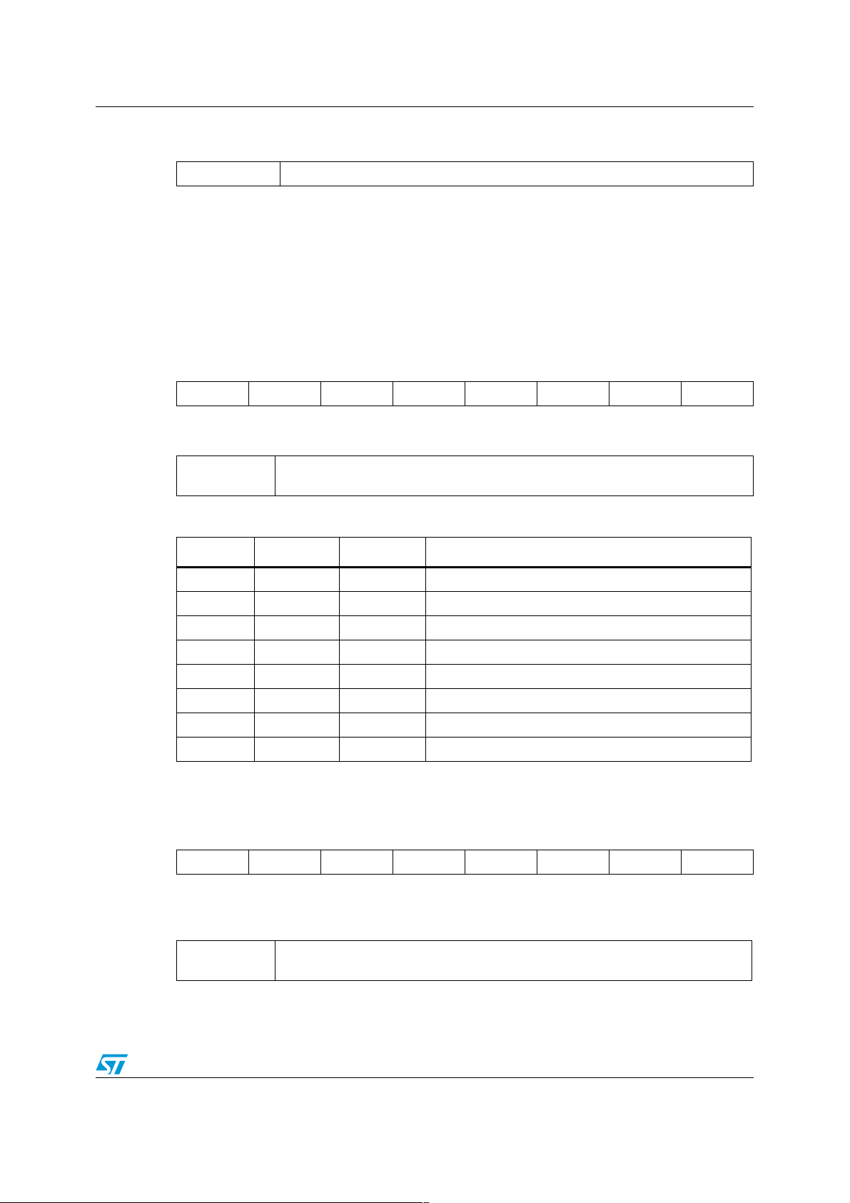
Table 53. INT2_DURATION_A description
D6 - D0 Duration value. Default value: 000 0000
The D6 - D0 bits set the minimum duration of the Interrupt 2 event to be recognized.
Duration time steps and maximum values depend on the ODR chosen.
9.2 Magnetic field sensing register description
9.2.1 CRA_REG_M (00h)
Table 54. CRA_REG_M register
(1)
0
1. This bit must be set to ‘0’ for correct working of the device.
Table 55. CRA_REG_M description
DO2 to DO0
(1)
0
(1)
0
DO2 DO1 DO0 0
(1)
(1)
0
Data output rate bits. These bits set the rate at which data is written to all three data
output registers (refer to Table 56). Default value: 100
Table 56. Data rate configurations
DO2 DO1 DO0 Minimum data output rate (Hz)
00 0 0.75
00 1 1.5
01 0 3.0
01 1 7.5
10 0 15
10 1 30
11 0 75
1 1 1 220
9.2.2 CRB_REG_M (01h)
Table 57. CRA_REG register
GN2 GN1 GN0 0
1. This bit must be set to ‘0’ for correct working of the device.
CRA_REG description
GN1-0
Gain configuration bits. The gain configuration is common for all channels (refer to
Table 58)
(1)
(1)
0
(1)
0
(1)
0
(1)
0
Doc ID 018725 Rev 1 33/38
Page 34
Register description LSM303DLM
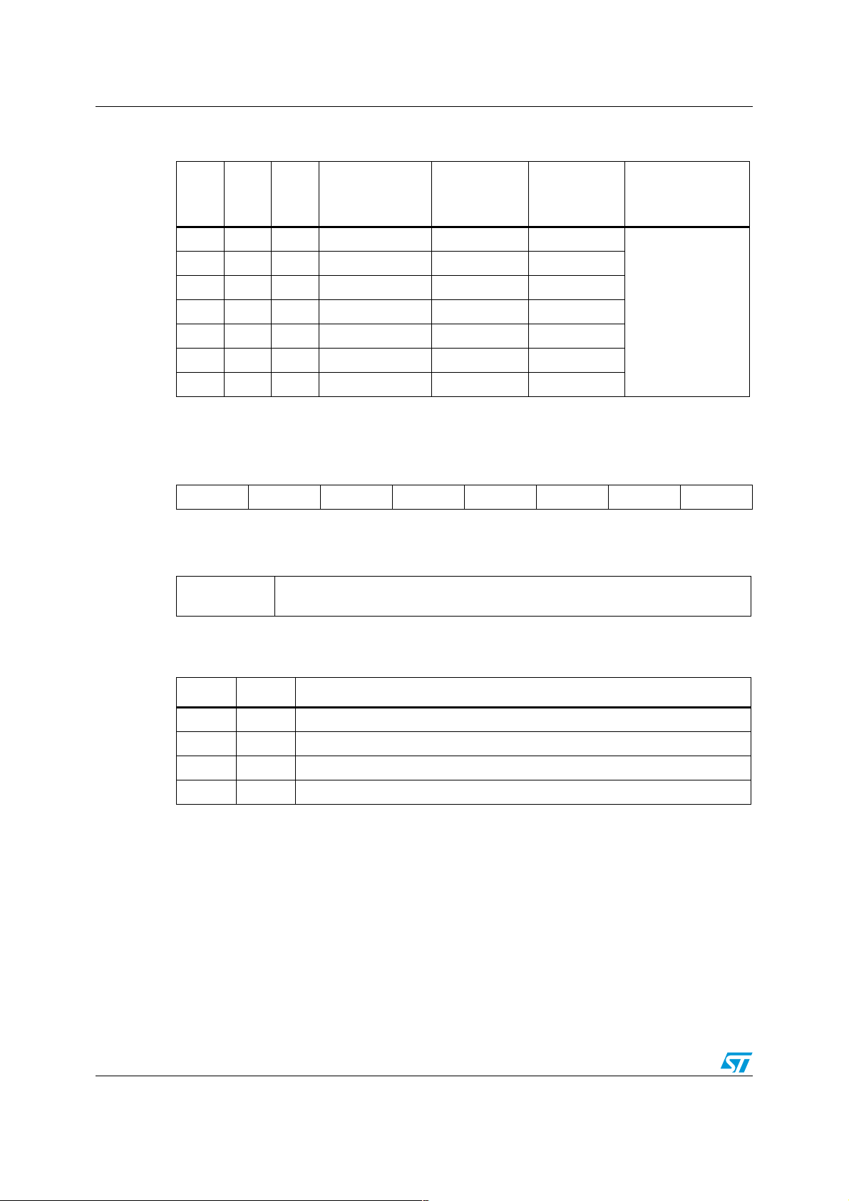
Table 58. Gain setting
GN2 GN1 GN0
0 0 1 ±1.3 1100 980
010 ±1.9 855 760
011 ±2.5 670 600
100 ±4.0 450 400
101 ±4.7 400 355
110 ±5.6 330 295
111 ±8.1 230 205
9.2.3 MR_REG_M (02h)
Table 59. MR_REG
(1)
0
1. This bit must be set to ‘0’ for correct working of the device
Table 60. MR_REG description
MD1-0
(1)
0
Mode select bits. These bits select the operation mode of this device (refer to
Table 61)
Sensor input
field range
[Gauss]
(1)
0
Gain X/Y and
[LSB/Gauss]
(1)
0
Z
(1)
0
Gain Z
[LSB/Gauss]
(1)
0
Output range
0xF800–0x07FF
(-2048–2047)
MD1 MD0
Table 61. Magnetic sensor operating mode
MD1 MD0 Mode
0 0 Continuous-conversion mode
0 1 Single-conversion mode
1 0 Sleep-mode. Device is placed in sleep-mode
1 1 Sleep-mode. Device is placed in sleep-mode
9.2.4 OUT_X_H_M (03), OUT_X_LH_M (04h)
X-axis magnetic field data. The value is expressed as 2’s complement.
9.2.5 OUT_Z_H_M (05), OUT_Z_L_M (06h)
Z-axis magnetic field data. The value is expressed as 2’s complement.
9.2.6 OUT_Y_H_M (07), OUT_Y_L_M (08h)
Y-axis magnetic field data. The value is expressed as 2’s complement.
34/38 Doc ID 018725 Rev 1
Page 35
LSM303DLM Register description
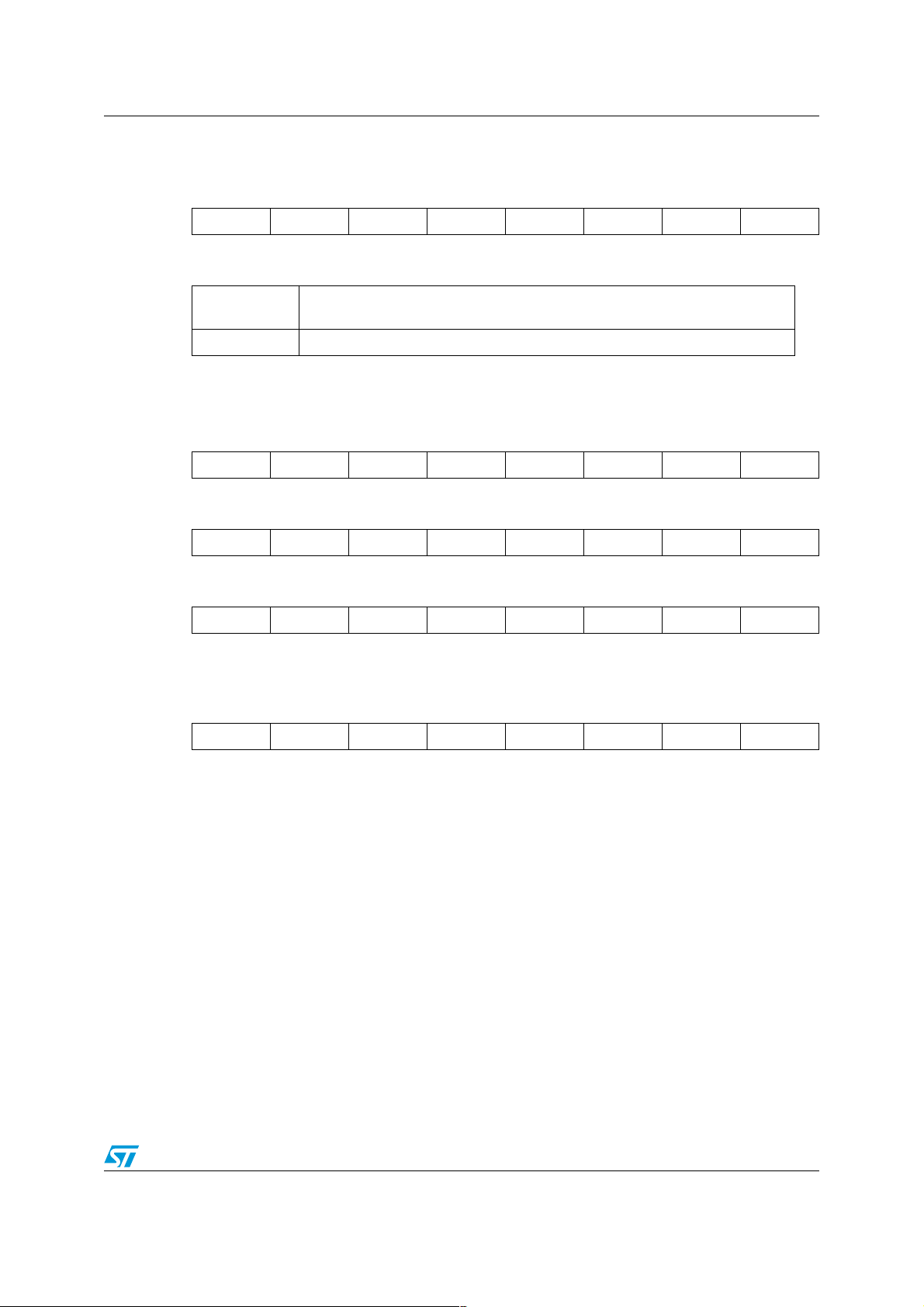
9.2.7 SR_REG_M (09h)
Table 62. SR register
-- -- -- -- -- -- LOCK DRDY
Table 63. SR register description
LOCK
DRDY Data ready bit. This bit is when a new set of measurements is available.
Data output register lock. Once a new set of measurements is available, this bit
is set when the first magnetic field data register has been read.
9.2.8 IR_REG_M (0Ah/0Bh/0Ch)
Table 64. IRA_REG_M
01001000
Table 65. IRB_REG_M
00110100
Table 66. IRC_REG_M
00110011
9.2.9 WHO_AM_I _M (0F)
Table 67. WHO_AM_I_M
00111100
Doc ID 018725 Rev 1 35/38
Page 36
Package information LSM303DLM
10 Package information
In order to meet environmental requirements, ST offers these devices in different grades of
ECOPACK
®
packages, depending on their level of environmental compliance. ECOPACK
specifications, grade definitions, and product status are available at: www.st.com.
ECOPACK is an ST trademark.
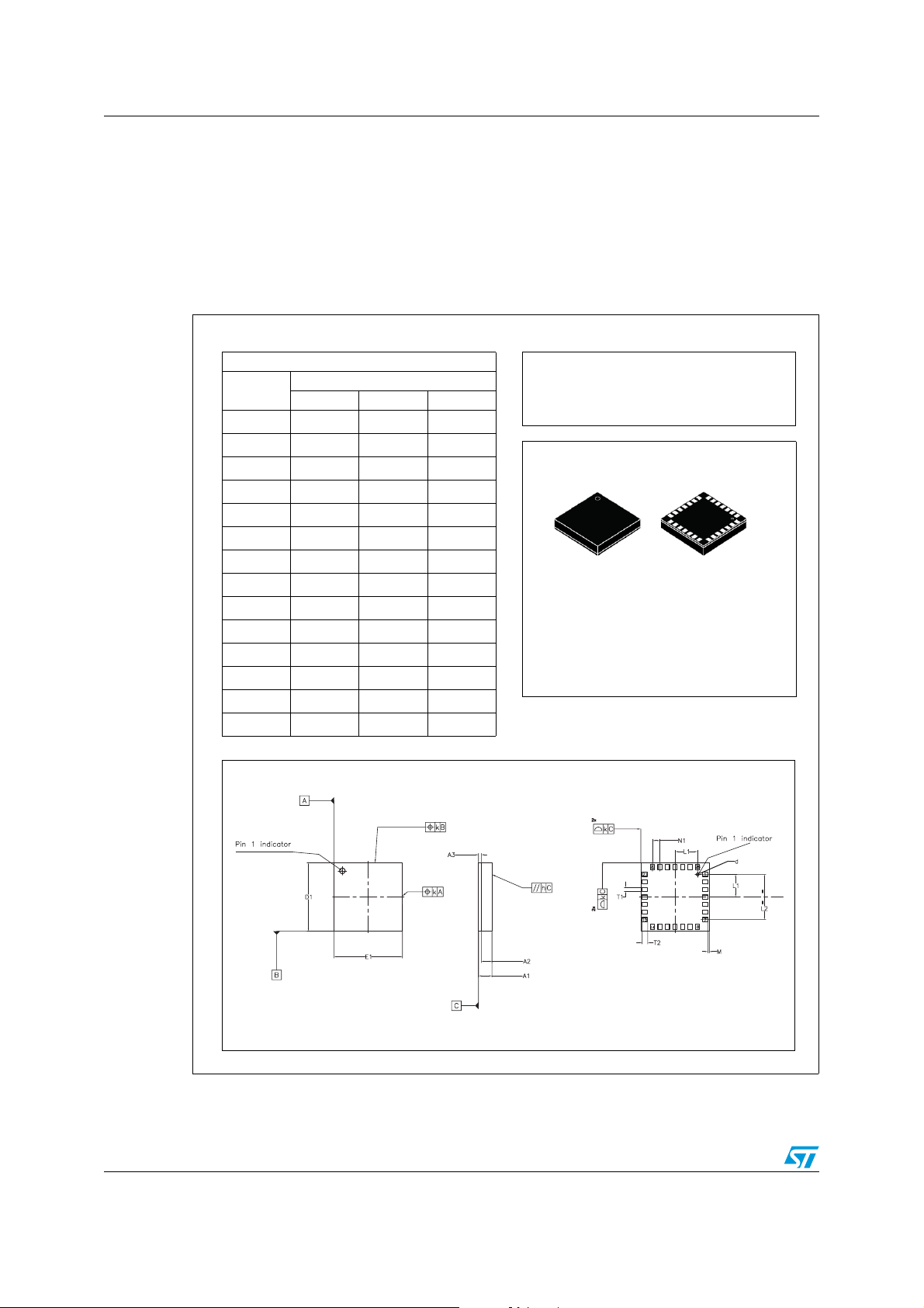
Figure 5. LGA-28: mechanical data and package dimensions
Dimensions
Ref.
A1 1
A2 0.785
A3 0.200
D1 4.850 5.000 5.150
E1 4.850 5.000 5.150
L1 1.650
L2 3.300
N1 0.550
M 0.040 0.100 0.160
T1 0.260 0.300 0.340
T2 0.360 0.400 0.440
d 0.200
k 0.050
h 0.100
Min. Typ. Max.
mm
Land Grid Array Packages
Outline and
mechanical data
LGA-28 (5x5x1)
36/38 Doc ID 018725 Rev 1
8192208_B
Page 37

LSM303DLM Revision history
11 Revision history
Table 68. Document revision history
Date Revision Changes
11-Apr-2011 1 Initial release.
Doc ID 018725 Rev 1 37/38
Page 38

LSM303DLM
Please Read Carefully:
Information in this document is provided solely in connection with ST products. STMicroelectronics NV and its subsidiaries (“ST”) reserve the
right to make changes, corrections, modifications or improvements, to this document, and the products and services described herein at any
time, without notice.
All ST products are sold pursuant to ST’s terms and conditions of sale.
Purchasers are solely responsible for the choice, selection and use of the ST products and services described herein, and ST assumes no
liability whatsoever relating to the choice, selection or use of the ST products and services described herein.
No license, express or implied, by estoppel or otherwise, to any intellectual property rights is granted under this document. If any part of this
document refers to any third party products or services it shall not be deemed a license grant by ST for the use of such third party products
or services, or any intellectual property contained therein or considered as a warranty covering the use in any manner whatsoever of such
third party products or services or any intellectual property contained therein.
UNLESS OTHERWISE SET FORTH IN ST’S TERMS AND CONDITIONS OF SALE ST DISCLAIMS ANY EXPRESS OR IMPLIED
WARRANTY WITH RESPECT TO THE USE AND/OR SALE OF ST PRODUCTS INCLUDING WITHOUT LIMITATION IMPLIED
WARRANTIES OF MERCHANTABILITY, FITNESS FOR A PARTICULAR PURPOSE (AND THEIR EQUIVALENTS UNDER THE LAWS
OF ANY JURISDICTION), OR INFRINGEMENT OF ANY PATENT, COPYRIGHT OR OTHER INTELLECTUAL PROPERTY RIGHT.
UNLESS EXPRESSLY APPROVED IN WRITING BY AN AUTHORIZED ST REPRESENTATIVE, ST PRODUCTS ARE NOT
RECOMMENDED, AUTHORIZED OR WARRANTED FOR USE IN MILITARY, AIR CRAFT, SPACE, LIFE SAVING, OR LIFE SUSTAINING
APPLICATIONS, NOR IN PRODUCTS OR SYSTEMS WHERE FAILURE OR MALFUNCTION MAY RESULT IN PERSONAL INJURY,
DEATH, OR SEVERE PROPERTY OR ENVIRONMENTAL DAMAGE. ST PRODUCTS WHICH ARE NOT SPECIFIED AS "AUTOMOTIVE
GRADE" MAY ONLY BE USED IN AUTOMOTIVE APPLICATIONS AT USER’S OWN RISK.
Resale of ST products with provisions different from the statements and/or technical features set forth in this document shall immediately void
any warranty granted by ST for the ST product or service described herein and shall not create or extend in any manner whatsoever, any
liability of ST.
ST and the ST logo are trademarks or registered trademarks of ST in various countries.
Information in this document supersedes and replaces all information previously supplied.
The ST logo is a registered trademark of STMicroelectronics. All other names are the property of their respective owners.
© 2011 STMicroelectronics - All rights reserved
STMicroelectronics group of companies
Australia - Belgium - Brazil - Canada - China - Czech Republic - Finland - France - Germany - Hong Kong - India - Israel - Italy - Japan -
Malaysia - Malta - Morocco - Philippines - Singapore - Spain - Sweden - Switzerland - United Kingdom - United States of America
www.st.com
38/38 Doc ID 018725 Rev 1
 Loading...