

Page 1
DEVICES INCORPORATED
LSH32
32-bit Cascadable Barrel Shifter
LSH32
DEVICES INCORPORATED
FEATURES DESCRIPTION
❑❑
❑ 32-bit Input, 32-bit Output Multi-
❑❑
plexed to 16 Lines
❑❑
❑ Full 0-31 Position Barrel Shift
❑❑
Capability
❑❑
❑ Integral Priority Encoder for 32-bit
❑❑
Floating Point Normalization
❑❑
❑ Sign-Magnitude or Two’s Comple-
❑❑
ment Mantissa Representation
❑❑
❑ 32-bit Linear Shifts with Sign or
❑❑
Zero Fill
❑❑
❑ Independent Priority Encoder
❑❑
Outputs for Block Floating Point
❑❑
❑ 68-pin PLCC, J-Lead
❑❑
The LSH32 is a 32-bit high speed
shifter designed for use in floating
point normalization, word pack/
unpack, field extraction, and similar
applications. It has 32 data inputs,
and 16 output lines. Any shift
configuration of the 32 inputs, including circular (barrel) shifting, left shifts
with zero fill, and right shift with sign
extend are possible. In addition, a
built-in priority encoder is provided
to aid floating point normalization.
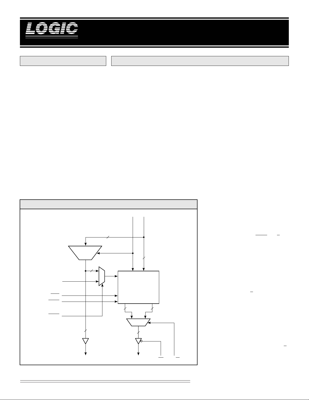
SHIFT ARRAY
The 32 inputs to the LSH32 are
applied to a 32-bit shift array. The 32
outputs of this array are multiplexed
down to 16 lines for presentation at
the device outputs. The array may be
LSH32 BLOCK DIAGRAM
SIGN
I
31-I0
32
32:5
PRIORITY
SI4-SI
RIGHT/LEFT
FILL/WRAP
NORM
ENCODE
5
0
5
SO4-SO
2:1
16 16
0
32
32-bit
BARREL
SHIFT
ARRAY
2:1
16
Y15-Y
0
32-bit Cascadable Barrel Shifter
configured such that any contiguous
16-bit field (including wraparound of
the 32 inputs) may be presented to the
output pins under control of the shift
code field (wrap mode). Alternatively, the wrap feature may be
disabled, resulting in zero or sign bit
fill, as appropriate (fill mode). The
shift code control assignments and the
resulting input to output mapping for
the wrap mode are shown in Table 1.
Essentially the LSH32 is configured as
a left shift device. That is, a shift code
of 000002 results in no shift of the
input field. A code of 000012 provides
an effective left shift of 1 position, etc.
When viewed as a right shift, the shift
code corresponds to the two’s complement of the shift distance, i.e., a
shift code of 111112 (–110) results in a
right shift of one position, etc.
When not in the wrap mode, the
LSH32 fills bit positions for which
there is no corresponding input bit.
The fill value and the positions filled
depend on the RIGHT/LEFT (R/L)
direction pin. This pin is a don’t care
input when in wrap mode. For left
shifts in fill mode, lower bits are filled
with zero as shown in Table 2. For
right shifts, however, the SIGN input
is used as the fill value. Table 3
depicts the bits to be filled as a
function of shift code for the right shift
case. Note that the R/L input changes
only the fill convention, and does not
affect the definition of the shift code.
In fill mode, as in wrap mode, the shift
code input represents the number of
shift positions directly for left shifts,
but the two’s complement of the shift
code results in the equivalent right
shift. However, for fill mode the R/L
OE
MS/LS
input can be viewed as the most
Special Arithmetic Functions
1
08/16/2000–LDS.32-Q
Page 2
DEVICES INCORPORATED
LSH32
32-bit Cascadable Barrel Shifter
TABLE 1. WRAP MODE SHIFT CODE DEFINITIONS
Shift CodeShift Code
Shift Code
Shift CodeShift Code
00000 I31 I30 I29 • • • I16 I 15 • • • I2 I1 I0
00001 I30 I29 I28 • • • I15 I 14 • • • I1 I0 I31
00010 I29 I28 I27 • • • I14 I 13 • • • I0 I31 I 30
00011 I28 I27 I26 • • • I13 I 12 • • • I31 I 30 I 29
• •••• • •• •• • ••••
• •••• • •• •• • ••••
• •••• • •• •• • ••••
01111 I16 I15 I14 • • • I1 I0• • •I19 I18 I17
10000 I15 I14 I13 • • • I0 I31 • • • I18 I 17 I16
10001 I14 I13 I12 • • • I31 I 30 • • • I17 I16 I15
10010 I13 I12 I11 • • • I30 I 29 • • • I16 I15 I14
• •••• • •• •• • ••••
• •••• • •• •• • ••••
• •••• • •• •• • ••••
11100 I3 I2 I1• • •I20 I 19 • • • I6 I5 I 4
11101 I2 I1 I0• • •I19 I 18 • • • I5 I4 I 3
11110 I1 I0 I31 • • • I18 I 17 • • • I4 I3 I2
11111 I0 I31 I30 • • • I17 I 16 • • • I3 I2 I1
YY
YY
3131
Y
31
3131
YY
YY
3030
30
3030
2929
Y
29
2929
YY
Y
YY
• • •• • •
• • •
• • •• • •
YY
YY
1616
16
1616
1515
Y
15 • • •
1515
YY
Y
YY
YY
YY
22
Y
2
22
YY
YY
11
Y
YY
00
1
Y
0
11
00
YY
TABLE 2. FILL MODE SHIFT CODE DEFINITIONS — LEFT SHIFT
Shift CodeShift Code
Shift Code
Shift CodeShift Code
00000 I31 I30 I29 • • • I16 I 15 • • • I2 I1 I0
00001 I30 I29 I28 • • • I15 I 14 • • • I1 I0 0
00010 I29 I28 I27 • • • I14 I 13 • • • I0 00
00011 I28 I27 I26 • • • I13 I 12 • • • 000
• •••• • •• •• • ••••
• •••• • •• •• • ••••
• •••• • •• •• • ••••
01111 I16 I15 I14 • • • I1 I0• • •000
10000 I15 I14 I13 • • • I0 0 • • • 000
10001 I14 I13 I12 • • • 00• • • 000
10010 I13 I12 I11 • • • 00• • • 000
• •••• • •• •• • ••••
• •••• • •• •• • ••••
• •••• • •• •• • ••••
11100 I3 I2 I1• • • 00• • • 000
11101 I2 I1 I0• • • 00• • • 000
11110 I1 I0 0 • • • 00• • • 000
11111 I0 00• • • 00• • • 000
YY
YY
3131
Y
31
3131
YY
YY
3030
30
3030
2929
Y
29
2929
YY
Y
YY
• • •• • •
• • •
• • •• • •
YY
YY
1616
16
1616
1515
Y
15 • • •
1515
YY
Y
YY
YY
YY
22
Y
2
22
YY
YY
11
Y
YY
00
1
Y
0
11
00
YY
significant bit of a 6-bit two’s complement shift code, comprised of R/L
concatenated with the SI4–SI0 lines.
Thus a positive shift code (R/L = 0)
results in a left shift of 0–31 positions,
and a negative code (R/L = 1) a right
shift of up to 32 positions. The LSH32
can thus effectively select any contiguous 32-bit field out of a (sign extended
and zero filled) 96-bit "input."
OUTPUT MULTIPLEXER
The shift array outputs are applied to
a 2:1 multiplexer controlled by the
MS/LS select line. This multiplexer
makes available at the output pins
either the most significant or least
significant 16 outputs of the shift
array.
PRIORITY ENCODER
The 32-bit input bus drives a priority
encoder which is used to determine
the first significant position for
purposes of normalization. The
priority encoder produces a five-bit
code representing the location of the
first non-zero bit in the input word.
Code assignment is such that the
priority encoder output represents the
number of shift positions required to
left align the first non-zero bit of the
input word. Prior to the priority
encoder, the input bits are individually exclusive OR’ed with the SIGN
input. This allows normalization in
floating point systems using two’s
complement mantissa representation.
A negative value in two’s complement
representation will cause the exclusive
OR gates to invert the input data to
the encoder. As a result the leading
significant digit will always be "1."
This affects only the encoder inputs;
the shift array always operates on the
raw input data. The priority encoder
function table is shown in Table 4.
ffs2
Special Arithmetic Functions
08/16/2000–LDS.32-Q
Page 3
DEVICES INCORPORATED
LSH32
32-bit Cascadable Barrel Shifter
TABLE 3. FILL MODE SHIFT CODE DEFINITIONS — RIGHT SHIFT
Shift CodeShift Code
Shift Code
Shift CodeShift Code
00000 S S S • • • SS• • •SSS
00001 S S S • • • SS• • •SSI31
00010 S S S • • • SS• • •SI31 I30
00011 S S S • • • SS• • •I31 I30 I 29
• •••• • •• •• • ••••
• •••• • •• •• • ••••
• •••• • •• •• • ••••
01111 S S S • • • SS• • •I19 I18 I 17
10000 S S S • • • SI31 • • • I18 I17 I16
10001 S S S • • • I31 I 30 • • • I17 I16 I15
10010 S S S • • • I30 I 29 • • • I16 I15 I14
• •••• • •• •• • ••••
• •••• • •• •• • ••••
• •••• • •• •• • ••••
11100 S S S • • • I20 I 19 • • • I6 I5 I4
11101 S S S • • • I19 I 18 • • • I5 I4 I3
11110 S S I31 • • • I18 I 17 • • • I4 I3 I 2
11111 S I31 I30 • • • I17 I 16 • • • I3 I2 I1
YY
YY
3131
Y
31
3131
YY
YY
3030
30
3030
2929
Y
29
2929
YY
Y
YY
• • •• • •
• • •
• • •• • •
YY
YY
1616
16
1616
1515
Y
15 • • •
1515
YY
Y
YY
YY
YY
22
Y
2
22
YY
YY
11
Y
YY
00
1
Y
0
11
00
YY
NORMALIZE MULTIPLXER
The NORM input, when asserted
results in the priority encoder output
driving the internal shift code inputs
directly. It is exactly equivalent to
routing the SO4–SO0 outputs back to
the SI4–SI0 inputs. The NORM input
provides faster normalization of 32-bit
data by avoiding the delay associated
with routing the shift code off chip.
When using the NORM function, the
LSH32 should be placed in fill mode,
with the R/L input low.
APPLICATIONS EXAMPLES
Normalization of mantissas up to 32
bits can be accomplished directly by a
single LSH32. The NORM input is
asserted, and fill mode and left shift
are selected. The normalized mantissa
is then available at the device output
in two 16-bit segments, under the
control of the output data multiplexer
select, the MS/LS.
TABLE 4. PRIORITY ENCODER FUNCTION TABLE
II
II
3131
I
31
3131
II
II
3030
30
3030
2929
I
29
2929
II
I
II
1XX• • • XX• • •X X X 00000
01X• • •XX• • •X X X 00001
001• • •XX• • •X X X 00010
•••• • •• •• • •••• •
•••• • •• •• • •••• •
000• • •1X• • • X X X 01111
000• • •01• • •X X X 10000
000• • •00• • •X X X 10001
•••• • •• •• • •••• •
•••• • •• •• • •••• •
000• • •00• • • 0 1 X 11110
000• • •00• • • 0 0 1 11111
000• • •00• • • 0 0 0 11111
• • •• • •
• • •
• • •• • •
II
II
1616
1515
I
16
1616
II
• • •• • •
I
15
• • •
1515
• • •• • •
II
II
II
II
22
I
II
11
2
I
1
22
11
II
Shift CodeShift Code
00
I
0
Shift Code
00
II
Shift CodeShift Code
If it is desirable to avoid the necessity
of multiplexing output data in 16-bit
segments, two LSH32 devices can be
used in parallel. Both devices receive
the same input word, with the MS/LS
select line of one wired high, and the
other low. Each device will then
independently determine the shift
distance required for normalization,
and the full 32 bits of output data will
be available simultaneously.
Special Arithmetic Functions
3
08/16/2000–LDS.32-Q
Page 4

DEVICES INCORPORATED
LSH32
32-bit Cascadable Barrel Shifter
LONG-WORD NORMALIZATION
(MULTIPLE CYCLES)
Normalization of floating point
mantissas longer than 32 bits can be
accomplished by cascading LSH32
units. When cascading for normalization, the device inputs are overlapped
such that each device lower in priority
than the first shares 16 inputs with its
more significant neighbor. Fill mode
and left shift are selected, however,
internal normalization (NORM) is not
used. The most significant result half
of each device is enabled to the
output. The shift out (SO4–SO0) lines
of the most significant slice are
connected to the shift in lines of all
slices, including the first. The exception is that all SI4 lines are grounded,
limiting the shift distance to 16
positions. The shift distance required
for normalization is produced by the
priority encoder in the most significant slice. The priority encoder will
produce the shift code necessary to
normalize the input word if the
leading non-zero digit is found in the
upper 16 bits. If this is the case, the
number of shift positions necessary to
accomplish normalization is placed on
the SO4 –SO0 outputs for use by all
slices, and the appropriate 0–15 bit
shift is accomplished. If the upper 16
bits are all zero, then the maximum
shift of 15 places is executed. Single
FIGURE 1. SINGLE CYCLE LONG-WORD NORMALIZATION USING LSH32S
I63-I
48
I47-I
32
I31-I
16
clock normalization requiring shifts
longer than 16 bits can be accomplished by a bank-select technique
described below.
SINGLE CYCLE LONG-WORD
NORMALIZATION
An extension of the above concept is a
single clock normalization of long
words (potentially requiring shifts of
more than 15 places). The arrangement of LSH32s required is shown in
Figure 1. Cascading of LSH32 units is
accomplished by connecting the SI3–
SI0 input lines of each unit to the SO3 –
SO0 outputs of the most significant
device in the row as before. Essen-
I15-I
0
0
PRIORITY
ENCODE
2:4
DECODE
MSBs
4
LSH32
3-0
SI
I
47-I32I31-I16
4
LSH32
SI
3-0
I
31-I16I15-I0
4
LSH32
SI
3-0
I
16-I0
4
LSH32
SI
3-0
SI
4
SO
SO
SO
SO
OE
OE
OE
0
OE
4-0
4-0
4-0
4-0
5
4
LSH32
SI
3-0
5
4
SI
3-0
5
4
SI
3-0
SI
4
5
OE
I15-I
LSH32
OE
0
LSH32
OE
4
LSH32
SI
3-0
0
4
SI
3-0
SI
4
OE
0
LSH32
OE
4
LSH32
SI
3-0
SI
4
OE
Y63-Y
48
Y47-Y
32
Y31-Y
16
Y15-Y
0
Special Arithmetic Functions
ffs4
08/16/2000–LDS.32-Q
Page 5

DEVICES INCORPORATED
LSH32
32-bit Cascadable Barrel Shifter
tially the LSH32s are arranged in
multiple rows or banks such that the
inputs to successive rows are leftshifted by 16 positions. The outputs
of each row are multiplexed onto a
three-state bus. The normalization
problem then reduces to selecting
from among the several banks that
one which has the first non-zero bit
of the input value among its 16 most
significant positions. If the most
significant one in the input file was
within the upper 16 locations of a
given bank, the SO4 output of the
most significant slice in that bank will
be low. Single clock normalization
can thus be accomplished simply by
enabling onto the three-state output
bus the highest priority bank in which
this condition is met. In this way the
input word will be normalized
regardless of the number of shift
positions required to accomplish this.
The number of shift positions can be
determined simply by concatenation
of the SO3–SO0 outputs of the most
significant slice in the selected row
with the encoded Output Enable-bits
determining the row number. Note
that lower rows need not be fully
populated. This is because they
represent left shifts in multiples of 16
positions, and the lower bits of the
output word will be zero filled. In
order to accomplish this zero fill, the
least significant device in each row is
always enabled, and the row select is
instead connected to the SI4 input.
This will force the shift length of the
least significant device to a value
greater than 15 whenever the row
containing that device is not selected.
This results in zero fill being accomplished by the equivalently positioned
slice in a higher bank, as shown in the
diagram.
BLOCK FLOATING POINT
With a small amount of external logic,
block floating point operations are
easily accomplished by the LSH32.
Data resulting from a vector operation
are applied to the LSH32 with the
NORM-input deasserted. The SO4–
SO0 outputs fill then represent the
normalization shift distance for each
vector element in turn. By use of an
external latch and comparator, the
maximum shift distance encountered
across all elements in the vector is
saved for use in the next block operation (or block normalization). During
this subsequent pass through the data,
the shift code saved from the previous
pass is applied uniformly across all
elements of the vector. Since the
LSH32 is not used in the internal
normalize mode, this operation can be
pipelined, thereby obtaining the
desired shift distance for the next pass
while simultaneously applying the
normalization required from the
previous pass.
Special Arithmetic Functions
5
08/16/2000–LDS.32-Q
Page 6

DEVICES INCORPORATED
LSH32
32-bit Cascadable Barrel Shifter
MAXIMUM RATINGS
Storage temperature ........................................................................................................... –65°C to +150°C
Operating ambient temperature........................................................................................... –55°C to +125°C
VCC supply voltage with respect to ground............................................................................ –0.5 V to +7.0V
Input signal with respect to ground ........................................................................................ –3.0 V to +7.0 V
Signal applied to high impedance output ............................................................................... –3.0 V to +7.0 V
Output current into low outputs............................................................................................................. 25 mA
Latchup current ............................................................................................................................... > 400 mA
OPERATING CONDITIONS
Active Operation, Commercial 0°C to +70°C 4.75 V ≤ VCC ≤ 5.25 V
Active Operation, Military –55°C to +125°C 4.50 V ≤ VCC ≤ 5.50 V
ELECTRICAL CHARACTERISTICS
Above which useful life may be impaired (Notes 1, 2, 3, 8)
To meet specified electrical and switching characteristics
Mode Temperature Range (Ambient) Supply Voltage
Over Operating Conditions (Note 4)
Symbol Parameter Test Condition Min Typ Max Unit
VOH Output High Voltage VCC = Min., IOH = –2.0 mA 2.4 V
VOL Output Low Voltage VCC = Min., IOL = 8.0 mA 0.4 V
VIH Input High Voltage 2.0 VCC V
V IL Input Low Voltage (Note 3) 0.0 0.8 V
IIX Input Current Ground ≤ VIN ≤ VCC (Note 12) ±20 µA
IOZ Output Leakage Current Ground ≤ VOUT ≤ VCC (Note 12) ±20 µA
ICC1 VCC Current, Dynamic (Notes 5, 6) 10 30 mA
ICC2 VCC Current, Quiescent (Note 7) 1.5 mA
ffs6
Special Arithmetic Functions
08/16/2000–LDS.32-Q
Page 7

DEVICES INCORPORATED
1234567890123456
1
6
1
6
1
6
1
6
1
6
1
6
1
6
1
6
1
6
1
6
1
6
1
6
1
6
1
6
1
6
1
6
1
6
1
6
1
6
1
6
1
6
1
6
1
6
1
6
1
6
1
6
1
6
1234567890123456
1234567890123456789012345678901212345678901234
1
4
1
4
1
4
1
4
1
4
1
4
1
4
1
4
1
4
1
4
1
4
1
4
1
4
1
4
1
4
1
4
1
4
1
4
1
4
1
4
1
4
1
4
1
4
1
4
1
4
1
4
1
4
1234567890123456789012345678901212345678901234
4
4
SWITCHING CHARACTERISTICS
LSH32
32-bit Cascadable Barrel Shifter
COMMERCIAL OPERATING RANGE (0°C to +70°C)
Symbol Parameter Min Max Min Max Min Max
tIY I, SIGN Inputs to Y Outputs 42 32 20
tIYN I, SIGN Inputs to Y Outputs, Normalize Mode 75 60 20
tISO I, SIGN Inputs to SO Outputs 55 42 20
tSIY SI, RIGHT/LEFT to Y Outputs 52 40 20
tMSY MS/LS Select to Y Outputs 28 24 15
tDIS Three-State Output Disable Delay (Note 11) 20 20 15
tENA Three-State Output Enable Delay (Note 11) 20 20 15
MILITARY OPERATING RANGE (–55°C to +125°C)
Symbol Parameter Min Max Min Max Min Max
tIY I, SIGN Inputs to Y Outputs 50 40 30
tIYN I, SIGN Inputs to Y Outputs, Normalize Mode 85 75 58
tISO I, SIGN Inputs to SO Outputs 65 52 42
tSIY SI, RIGHT/LEFT to Y Outputs 62 52 40
tMSY MS/LS Select to Y Outputs 32 26 24
tDIS Three-State Output Disable Delay (Note 11) 22 20 17
tENA Three-State Output Enable Delay (Note 11) 22 20 17
Notes 9, 10 (ns)
23456789012345
23456789012345
23456789012345
23456789012345
23456789012345
23456789012345
23456789012345
23456789012345
23456789012345
23456789012345
23456789012345
23456789012345
23456789012345
23456789012345
23456789012345
23456789012345
23456789012345
23456789012345
23456789012345
23456789012345
23456789012345
23456789012345
23456789012345
23456789012345
23456789012345
23456789012345
23456789012345
Notes 9, 10 (ns)
23456789012345678901234567890121234567890123
23456789012345678901234567890121234567890123
23456789012345678901234567890121234567890123
23456789012345678901234567890121234567890123
23456789012345678901234567890121234567890123
23456789012345678901234567890121234567890123
23456789012345678901234567890121234567890123
23456789012345678901234567890121234567890123
23456789012345678901234567890121234567890123
23456789012345678901234567890121234567890123
23456789012345678901234567890121234567890123
23456789012345678901234567890121234567890123
23456789012345678901234567890121234567890123
23456789012345678901234567890121234567890123
23456789012345678901234567890121234567890123
23456789012345678901234567890121234567890123
23456789012345678901234567890121234567890123
23456789012345678901234567890121234567890123
23456789012345678901234567890121234567890123
23456789012345678901234567890121234567890123
23456789012345678901234567890121234567890123
23456789012345678901234567890121234567890123
23456789012345678901234567890121234567890123
23456789012345678901234567890121234567890123
23456789012345678901234567890121234567890123
23456789012345678901234567890121234567890123
23456789012345678901234567890121234567890123
42
50
LSH32–
*
32 20
LSH32–
*
40
*
30
*
SWITCHING WAVEFORMS
I
31-I0
SIGN
SI
4
-SI
SO
MS/LS
4
-SO
Y
31-Y0
OE
Y
31-Y0
0
0
t
DIS
RIGHT/LEFT
2345678901234567890123
2345678901234567890123
*DISCONTINUED SPEED GRADE
t
IY,tIYN
t
t
ISO
t
SIY
HIGH IMPEDANCE
t
ENA
Special Arithmetic Functions
7
MSY
08/16/2000–LDS.32-Q
Page 8

DEVICES INCORPORATED
OE
0.2 V
t
DIS
t
ENA
0.2 V
1.5 V 1.5 V
3.5V Vth
1
Z
0
Z
Z
1
Z
0
1.5 V
1.5 V
0V Vth
VOL*
V
OH
*
V
OL
*
V
OH
*
Measured V
OL
with IOH = –10mA and IOL = 10mA
Measured V
OH
with IOH = –10mA and IOL = 10mA
NOTES
LSH32
32-bit Cascadable Barrel Shifter
1. Maximum Ratings indicate stress
specifications only. Functional operation of these products at values beyond
those indicated in the Operating Conditions table is not implied. Exposure to
maximum rating conditions for extended periods may affect reliability.
2. The products described by this specification include internal circuitry designed to protect the chip from damaging substrate injection currents and accumulations of static charge. Nevertheless, conventional precautions should
be observed during storage, handling,
and use of these circuits in order to
avoid exposure to excessive electrical
stress values.
3. This device provides hard clamping of
transient undershoot and overshoot. Input levels below ground or above VCC
will be clamped beginning at –0.6 V and
VCC + 0.6 V. The device can withstand
indefinite operation with inputs in the
range of –0.5 V to +7.0 V. Device operation will not be adversely affected, however, input current levels will be well in
excess of 100 mA.
9. AC specifications are tested with
input transition times less than 3 ns,
output reference levels of 1.5 V (except
tDIS test), and input levels of nominally
0 to 3.0 V. Output loading may be a
resistive divider which provides for
specified IOH and IOL at an output
voltage of VOH min and VOL max
respectively. Alternatively, a diode
bridge with upper and lower current
sources of IOH and IOL respectively,
and a balancing voltage of 1.5 V may be
used. Parasitic capacitance is 30 pF
minimum, and may be distributed.
This device has high-speed outputs capable of large instantaneous current
pulses and fast turn-on/turn-off times.
As a result, care must be exercised in the
testing of this device. The following
measures are recommended:
a. A 0.1 µF ceramic capacitor should be
installed between VCC and Ground
leads as close to the Device Under Test
(DUT) as possible. Similar capacitors
should be installed between device VCC
and the tester common, and device
ground and tester common.
11. For the tENA test, the transition is
measured to the 1.5 V crossing point
with datasheet loads. For the tDIS test,
the transition is measured to the
±200mV level from the measured
steady-state output voltage with
±10mA loads. The balancing voltage, VTH, is set at 3.5 V for Z-to-0
and 0-to-Z tests, and set at 0 V for Zto-1 and 1-to-Z tests.
12. These parameters are only tested at
the high temperature extreme, which is
the worst case for leakage current.
FIGURE A. OUTPUT LOADING CIRCUIT
DUT
S1
I
OL
V
C
L
I
TH
OH
FIGURE B. THRESHOLD LEVELS
4. Actual test conditions may vary from
those designated but operation is guaranteed as specified.
5. Supply current for a given application can be accurately approximated by:
2
NCV F
where
4
N = total number of device outputs
C = capacitive load per output
V = supply voltage
F = clock frequency
b. Ground and VCC supply planes
must be brought directly to the DUT
socket or contactor fingers.
c. Input voltages should be adjusted to
compensate for inductive ground and VCC
noise to maintain required DUT input
levels relative to the DUT ground pin.
10. Each parameter is shown as a minimum or maximum value. Input requirements are specified from the point
of view of the external system driving
the chip. Setup time, for example, is
specified as a minimum since the exter-
6. Tested with all outputs changing every cycle and no load, at a 5 MHz clock
rate.
nal system must supply at least that
much time to meet the worst-case requirements of all parts. Responses from
the internal circuitry are specified from
7. Tested with all inputs within 0.1 V of
VCC or Ground, no load.
8. These parameters are guaranteed
but not 100% tested.
the point of view of the device. Output
delay, for example, is specified as a
maximum since worst-case operation of
any device always provides data within
that time.
Special Arithmetic Functions
ffs8
08/16/2000–LDS.32-Q
Page 9

DEVICES INCORPORATED
7
7
7
7
7
7
7
7
7
7
7
7
7
7
7
7
7
7
7
7
7
7
7
7
7
7
7
7
7
7
7
7
7
7
7
7
7
7
7
7
7
7
7
7
7
7
7
7
7
7
7
7
7
7
7
7
7
7
7
7
7
7
7
7
7
7
7
LSH32
32-bit Cascadable Barrel Shifter
Speed
32 ns
20 ns
ORDERING INFORMATION
68-pin
I29I28I27I26I25I24I23I22I21I20I19I18I17I16I15I14GND
3
46663 6212
I
I
SIGN
SO
SO
SO
SO
SO
NORM
SI
SI
SI
SI
SI
R/L
F/W
31/15
Y
10
30
11
31
12
13
4
14
3
15
2
16
1
17
0
18
19
4
20
3
21
2
22
1
23
0
24
25
26
27 32 33 34 35 36 37 386139 40941 42 43
28 29 30 31
30/14Y29/13Y28/12Y27/11Y26/10
Y
5867
25/9Y24/8Y23/7Y22/6Y21/5Y20/4Y19/3Y18/2Y17/1Y16/0
Y
Plastic J-Lead Chip Carrier
0°C to +70°C — COMMERCIAL SCREENING
LSH32JC32
LSH32JC20
–55°C to +125°C — COMMERCIAL SCREENING
–55°C to +125°C — MIL-STD-883 COMPLIANT
Top
View
(J2)
6768 6465
OE
60
59
58
57
56
55
54
53
52
51
50
49
48
47
46
45
44
MS/LS
23456789012345678901234567890121234567890123456
23456789012345678901234567890121234567890123456
23456789012345678901234567890121234567890123456
68-pin
23456789012345678901234567890121234567890123456
23456789012345678901234567890121234567890123456
23456789012345678901234567890121234567890123456
23456789012345678901234567890121234567890123456
23456789012345678901234567890121234567890123456
23456789012345678901234567890121234567890123456
23456789012345678901234567890121234567890123456
23456789012345678901234567890121234567890123456
23456789012345678901234567890121234567890123456
23456789012345678901234567890121234567890123456
23456789012345678901234567890121234567890123456
23456789012345678901234567890121234567890123456
23456789012345678901234567890121234567890123456
23456789012345678901234567890121234567890123456
23456789012345678901234567890121234567890123456
23456789012345678901234567890121234567890123456
GND
23456789012345678901234567890121234567890123456
13
I
23456789012345678901234567890121234567890123456
23456789012345678901234567890121234567890123456
I
12
23456789012345678901234567890121234567890123456
23456789012345678901234567890121234567890123456
I
11
23456789012345678901234567890121234567890123456
23456789012345678901234567890121234567890123456
I
10
23456789012345678901234567890121234567890123456
23456789012345678901234567890121234567890123456
I
9
23456789012345678901234567890121234567890123456
23456789012345678901234567890121234567890123456
I
8
23456789012345678901234567890121234567890123456
23456789012345678901234567890121234567890123456
I
7
23456789012345678901234567890121234567890123456
23456789012345678901234567890121234567890123456
I
6
23456789012345678901234567890121234567890123456
23456789012345678901234567890121234567890123456
I
5
23456789012345678901234567890121234567890123456
I
4
23456789012345678901234567890121234567890123456
23456789012345678901234567890121234567890123456
I
3
23456789012345678901234567890121234567890123456
23456789012345678901234567890121234567890123456
I
2
23456789012345678901234567890121234567890123456
23456789012345678901234567890121234567890123456
I
1
23456789012345678901234567890121234567890123456
23456789012345678901234567890121234567890123456
I
0
23456789012345678901234567890121234567890123456
23456789012345678901234567890121234567890123456
V
CC
23456789012345678901234567890121234567890123456
23456789012345678901234567890121234567890123456
V
CC
23456789012345678901234567890121234567890123456
23456789012345678901234567890121234567890123456
23456789012345678901234567890121234567890123456
23456789012345678901234567890121234567890123456
23456789012345678901234567890121234567890123456
23456789012345678901234567890121234567890123456
23456789012345678901234567890121234567890123456
23456789012345678901234567890121234567890123456
23456789012345678901234567890121234567890123456
23456789012345678901234567890121234567890123456
23456789012345678901234567890121234567890123456
23456789012345678901234567890121234567890123456
23456789012345678901234567890121234567890123456
23456789012345678901234567890121234567890123456
23456789012345678901234567890121234567890123456
23456789012345678901234567890121234567890123456
23456789012345678901234567890121234567890123456
23456789012345678901234567890121234567890123456
1234567 8 9 10 11
A
I
29
I
28
I
26
I
24
I
22
I
20
I
18
B
I
30
I
I
31
27
I
25
I
23
I
21
I
19
I
17
C
SIGN
SO
4
D
3
SO
2
SO
SO
SO
1
0
NORM
SI
4
Top View
Through Package
(i.e., Component Side Pinout)
E
F
G
3
SI
2
SI
H
SI
1
SI
0
J
R/L
F/W
K
30/14
Y
Y
31/15
28/12
Y
Y
26/10
Y
24/8
Y
22/6
Y
20/4
Y
18/2
L
Y
29/13
Y
27/11
Y
25/9
Y
23/7
Y
21/5
Y
19/3
Y
17/1
Discontinued Package
Y
Ceramic Pin Grid Array
(G1)
Special Arithmetic Functions
9
I
I
16
14
I
15
GND
GND
12
I
13
I
I
10
I
11
I
8
I
9
I
6
I
7
I
4
I
5
I
2
I
3
I
0
I
1
16/0
V
CC
V
CC
MS/LS
OE
08/16/2000–LDS.32-Q
 Loading...