

Page 1
现货库存、技术资料、百科信息、热点资讯,精彩尽在鼎好!
LM1893/LM2893 Carrier-Current Transceiver
April 1995
LM1893/LM2893 Carrier-Current Transceiver
General Description
Carrier-current systems use the power mains to transfer information between remote locations. This bipolar carriercurrent chip performs as a power line interface for half-duplex (bi-directional) communication of serial bit streams of
virtually any coding. In transmission, a sinusoidal carrier is
FSK modulated and impressed on most any power line via a
rugged on-chip driver. In reception, a PLL-based demodulator and impulse noise filter combine to give maximum range.
A complete system may consist of the LM1893, a COPS
controller, and discrete components.
Features
Y
Noise resistant FSK modulation
Y
User-selected impulse noise filtering
Y
Up to 4.8 kBaud data transmission rate
Y
Strings of 0’s or 1’s in data allowed
Y
Sinusoidal line drive for low RFI
Typical Application
Y
Output power easily boosted 10-fold
Y
50 to 300 kHz carrier frequency choice
Y
TTL and MOS compatible digital levels
Y
Regulated voltage to power logic
Y
Drives all conventional power lines
Applications
Y
Energy management systems
TM
Y
Home convenience control
Y
Inter-office communication
Y
Appliance control
Y
Fire alarm systems
Y
Security systems
Y
Telemetry
Y
Computer terminal interface
²
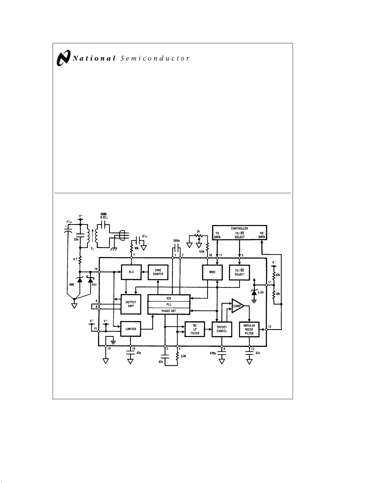
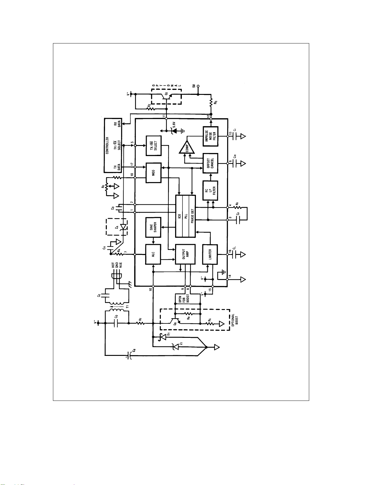
FIGURE 1. Block diagram of carrierÐcurrent chip with a complement of discrete components making a complete
e
F
125 kHz, f
O
BI-LINETMand COPSTMare trademarks of National Semiconductor Corp.
²
Carrier-Current Transceivers are also called Power Line Carrier (PLC) transceivers.
C
1995 National Semiconductor Corporation RRD-B30M115/Printed in U. S. A.
e
360 Baud transceiver. Use caution with this circuitÐdangerous line voltage is present.
DATA
TL/H/6750
TL/H/6750– 1
Page 2

Absolute Maximum Ratings
If Military/Aerospace specified devices are required,
please contact the National Semiconductor Sales
Office/Distributors for availability and specifications.
Supply voltage 30 V
Voltage on pin 12 55 V
Voltage on pin 10 (Note 1) 41 V
Voltage on pins 5 and 17 40 V
5.6 V DC zener current 100 mA
Junction temperature: transmit mode 150
Electro-Static Discharge (120 pF, 1500X) 1KV
receive mode 125
Maximum continuous dissipation, T
plastic DIP N (Note 2): transmit mode 1.66 W
Operating ambient temp. range
Storage temperature range
Lead temp., soldering, 7 seconds 260
Absolute maximum ratings indicate limits beyond
Note:
which damage to the device may occur. Electrical specifications are not ensured when operating the device above
C
§
§
guaranteed limits but below absolute maximum limits, but
C
there will be no device degradation.
receive mode 1.33 W
e
25§C,
A
b
40 to 85§C
b
65 to 150§C
C
§
General Electrical Characteristics
(Note 3). The test conditions are: V
Ý
1 5.6 V Zener voltage, V
Parameter Conditions Typical Limit Limit
Z
2 5.6 V Zener resistance, R
3 Carrier I/O peak survivable Pin 10, discharge 1 mF cap. charged to V
transient voltage, V
OT
4 Carrier I/O clamp voltage, V
5 Carrier I/O clamp resistance, R10Pin 10, I
6 TX/RX low input voltage, V
7 TX/RX high input voltage, V
8 TX/RX low input current, I
9 TX/RX high input current, I
10 RXbTX switch-over time, T
11 TXbRX switch-over time, T
12 ICO initial accuracy of F
O
13 ICO temperature coefficient of FOTX or RX mode, (F
14 Temperature drift of F
O
Transmitter Electrical Characteristics (Note 3). The test conditions are: V
unless otherwise noted. The transmit center frequency is F
Ý
15 Supply voltage, Va, range Meets test 17 spec. at T
16 Total supply current, I
17 Carrier I/O output current, I
18 Carrier I/O lower swing limit, V
19 THD of IO(Note 6) Q of 10 tank driving 10X line 0.6 5.0 % max.
20 FSK deviation, F
21 Data In. low input voltage, V
22 Data In. high input voltage, V
23 Data In. low input current, I
24 Data In. high input current, I
Parameter Conditions Typical Limit Limit
QT
b
F
2
1
a
e
18V and F
Pin 11, I
Z
Pin 11, R
thruk1X
Pin 10, I
OC
2N2222 diode pin 8 to 9 50 V max.
Pin 5 1.8 0.8 V max.
IL
Pin 5 (Note 9) 2.2 2.8 V min.
IH
IL
IH
Pin 5 at 0.8 V
Pin5at40V
Time to develop 63% of full current drive thru pin 10 10 ms
RT
1 bit time, T
TR
controlled with C
TX mode, R
e
F
0
TX or RX mode,b40sT
(F
l
(F
l
Pin 15. Pin 12 high. IQTis IQthrough 52 79 mA max.
pin 15 and the average current I
Carrier I/O through pin 10
O
100X load on pin 10 70 45 mApp min.
Pin 10. Set internally be ALC. 4.7 4.0 V min.
ALC
2N2222 diode pin 8 to 9 5.7 V max.
e
125 kHz, unless otherwise noted.
O
Test Design
(Note 4) (Note 5)
e
2 mA 5.6 5.2 V min.
Z
@
e
(V
10 mAbV
Z
Z
e
10 mA, RX mode 44 41 V min.
OC
e
10 mA 20 X
OC
e
1/(2F
B
M
e
6.65 kX,C
O
a
(F
F2)/2 137 kHz max.
1
@
1 mA)/(10 mAb1 mA) 5 X
Z
). Time TTRis user 2 bit
DATA
, see Apps. Info.
O
b
F
OMAX
OMIN
s
T
J
JMAX
, FSK low is F1, and FSK high is F2.
O
OT
e
560 pF 125 113 kHz min.
b
)/(T
T
JMAX
JMIN
80 60 V max.
b
b
10
b
)
100 PPM/§C
g
2.0
5.9 V max.
b
2
20 mA min.
1 mA max.
b
4
1 0 mA min.
10 mA max.
a
e
18 V and F
g
5.0 % max.
e
125 kHz
O
Test Design
(Note 4) (Note 5)
e
25§C and: 13 14 15 V min.
J
b
[
]
[
F
14V
[
24V
18V])/F
1
b
]
[
F
18V])/F
1
1
1
k
[
]
0.01 40 24 23 V max.
18V
l
1
k
[
]
0.01
18V
l
1
of the
ODC
Limit
Units
Limit
Units
100X load, no tank 5.5 9 % max.
b
a
(F
F1)/([F
2
IL
IH
IL
IH
Pin 17 1.7 0.8 V max.
Pin 17 (Note 9) 2.1 2.8 V min.
Pin 17 at 0.8 V
Pin 17 at 40 V
]
F
/2) 4.4 3.7 % min.
2
1
b
1
b
10
5.2 % max.
b
10 mA min.
1 mA max.
b
4
1 0 mA min.
10 mA max.
2
Page 3

a
(Note 4) (Note 5)
40
45
e
Test Design
g
g
Receiver Electrical Characteristics (Note 3). The test conditions are: V
deviation FSK, F
Ý
25 Supply voltage, Va, range Functional receiver (Note 7) 12 13 13.5 V min.
26 Supply current, I
27 Carrier I/O input resistance, R
28 Max. data rate, F
29 PLL capture range, F
30 PLL lock range, F
31 Receiver input sensitivity, S
32 Tolerable input dc voltage offset Pin 10 lower than pin 15 by V
range, V
DATA
e
2.4 kHz, V
e
100 mVpp, in the receive mode, unless otherwise noted.
IN
Parameter Conditions Typical Limit Limit
37 30 28 V max.
QT
10
MD
C
L
IN
INDC
IQTis pin 15 (Va) plus pin 10 11 5 mA min.
(Carrier I/O) current. 2.4 kX Pin 13 to GND. 14 mA max.
Pin 10 19.5 14 kX min.
Functional receiver (Note 7), C
e
0X, no tank,
R
F
e
4.8 kBaud
2.4 kHz
e
C
F
e
C
F
For a functional receiver (Note 8)
Referred to chip side (pin 10) 1.8 10 12 mV
of the line-coupling XFMR: F
Referred to line side of XFMR: 0.26 mV
(assuming a 7.07:1 XFMR) F
100 pF, R
100 pF, R
e
0 X
F
e
0 X
F
e
100 pF, 10 4.8 2.4 kBaud
F
g
g
e
50 kHz 2.0 mV
O
e
F
300 kHz 1.4 mV
O
e
50 kHz 0.29 mV
O
e
F
300 kHz 0.20 mV
O
INDC
2 0.1 V max.
e
18 V, F
125 kHz,g2.2%
O
Limit
Units
30 kX max.
15
g
10 % min.
15 % min.
RMS
RMS
RMS
RMS
RMS
RMS
33 Data Out. breakdown voltage Pin 12, leakage Is20 mA 70 55 V min.
e
g
V
OH
e
2 mA 0.15 0.4 V max.
OL
g
55
g
45 mA min.
g
85 mA max.
3.5 V max.
e
g
250 mV
a
WINDOW
to above 2.8 V.
DC offset 0.95 0.70 V/V min.
g
55
b
0.5
C to insure that the junction temperature remains below the
§
(fundamental)].
RMS
DATA
g
25 mA min.
g
80 mA max.
b
20
e
1.2 kHz, (2) all of the data transitions must fall
b
40 nA min.
e
e
T
25§C. Pin
A
J
34 Data Out. low output, V
35 Impulse noise filter current, I
OL
I
36 Offset hold cap. bias voltage, V
37 Offset hold capacitor max. drive Pin 6. V(pin 3)bV(pin 4)
current, I
R
PD
voltage, V
-to-V
PD
MCM
PD
ratio, VW/V
OHB
PC
PD
38 Offset hold bias current, I
39 Phase comparator current, I
40 Phase detector output resistance, Pins 3 and 4. 10 6 kX min.
41 Phase detector demodulated output Pin 3 to 4, measured after filtering 100 60 mVpp min.
42 Fast offset cancel voltage ‘‘window’’ V
43 Power supply rejection, PSRR C
Note 1: More accurately, the maximum voltage allowed on pin 10 is VOC, and VOCranges from 41 to 50V. Also, transients may reach above 60V; see the transient
peak voltage characteristic curve.
Note 2: The maximum power dissipation rating should be derated for device operation above 25
maximum rating. Use a i
detail.
Note 3: The boldface values apply over the full junction temperature range for the specified supply voltage range. All other numbers apply at T
numbers refer to LM1893. LM2893 tested by shorting Carrier In to Carrier Out and testing it as an LM1893.
Note 4: Guaranteed and 100% production tested.
Note 5: Guaranteed (but not 100% production tested) over the temperature and supply voltage ranges. These limits are not used to calculate outgoing quality
levels.
Note 6: Total harmonic distortion is measured using THD
Note 7: Receiver function is defined as the error-free passage of 1 cycle of 50% duty-cycle 2.4 kHz square-wave data (2 sequential 208 mS bits), with the first bit
being a ‘‘1.’’ All of the data transitions (edges) must fall within
filter cap. C
Note 8: During the sensitivity check, note 7 requirements are followed with these exceptions: (1) data rate F
within
approximately 6200 pF).
Note 9: For TTL compatibility use a pull-up resistor to increase min. V
for this test.
I
g
20% (g41.6 ms) of their noise-free positions, and (3), a time-domain filter capacitor (CI) is used. The time delay of CIis (/2 bit, or 208 ms. (CIis
of 75§C/W for the N package using a socket in still air (which is the worst case). Consult the Application Information section for more
JA
Pin 12, sat. voltage at I
Pin 13 charge and discharge current
Pin 6 2.0 1.3 V min.
CM
Pin 6, TX mode. Bias pin 6 as it selfbiased during test 31. 40 nA max.
Bias pins 3 and 4 at 8.5 V 100 50 mA min.
e
I
I(pin 3)aI(pin 4), TX mode 200 mA max.
PC
e
R
(V@100mAbV@50mA)/(50mA) 18 kX max.
PD
out the 2FOcomponent 180 mVpp max.
b
V
PIN3
PIN4
Drive forg1 mA pin 6 current 1.20 V/V max.
e
0.1 mF. PSRReCMRR. 120 Hz 80 dB min.
L
e
[
(all components at or above 2FO)]/[I
I
RMS
g
10% (g20.8 ms) of their noise-free positions. RX time delay is minimized by using no impulse noise
3
Page 4
Typical Performance Characteristics (V
LM1893)
a
e
18V, F
e
125 kHz, circuit of
O
Figure 1
, pin numbers for
Total Current Consumption,
, vs Supply Voltage
I
QT
Chip Bias Current, I
vs Junction Tempurature
,
Q
Transient Voltage Survival
vs Pulse Time
Total Current Consumption,
IQT, vs Junction Temperature
Output Stage DC Current,
I
, vs Output Voltage
ODC
Transmitter AC Output Current
vs Junction Temperature
Chip Bias Current,
iQ, vs Supply Voltage
Output Stage DC Current,
I
,vs
ODC
Junction Temperature
Transmitter Sinusoid THD
vs Junction Temperature
ALC Voltage vs
Junction Temperature
ICO Frequency vs
Junction Temperature
4
Transmitter FSK Deviation
vs Junction Temperature
TL/H/6750– 38
Page 5
Typical Performance Characteristics (Continued)
Maximum Data Rate vs
Junction Temperature
PLL Capture & Lock Range vs
Junction Temperature
Impulse Noise Filter
Current vs Junction
Temperature
Receiver Sensitivity vs
Junction Temperature
Receiver Sensitivity vs
PLL Lock Range and F
Phase Detector Output
Voltage vs Junction
Temperature
PLL Lock Range vs
Junction Temperature and F
Receiver Sensitivity vs
O
PLL Lock Range and Loop Filter
Offset Hold Cap. Charge
Currents vs Junction
Temperature
O
Offset Hold Cap. Bias Current vs
Junction Temperature
Data Out. Low Voltage vs
Pull Down Current
5
Pin 7 Bias Voltage vs
Junction Temperature
TL/H/6750– 39
Page 6
Application Information*
THE DATA PATH
The BI-LINETMchip serves as a power line interface in the
carrier-current transceiver (CCT) system of
4
shows the interface circuit now discussed. The controller
may select either the transmit (TX) or receive (RX) mode.
Serial data from the controller is used to generate a FSKmodulated 50 to 300 kHz carrier on the line in the TX mode.
In the RX mode line signal passes through the coupling
transformer into the PLL-based receiver. The recreated serial bit stream drives the controller.
With the IC in the TX mode (pin 5 a logic high), baseband
data to 5 kHz drive the modulator’s Data In pin to generate
a switched 0.978I/1.022I control current to drive the low TC,
triangle-wave, current-controlled oscillator to
tion. The tri-wave passes through a differential attenuator
and sine shaper which deliver a current sinusoid through an
automatic level control (ALC) circuit to the gain of 200 current output amplifier. Drive current from the Carrier I/O develops a voltage swing on T
proportional to line impedance, then passes through the
’s (
1
step-down transformer and coupling capacitor C
line. Progressively smaller line impedances cause reduced
signal swing, but never clipping-thus avoiding potential radio
frequency interference. When large line impedances threaten to allow excessive output swing on pin 10, the ALC
shunts current away from the output amplifier, holding the
voltage swing constant and within the amp’s compliance
limit. The amplifier is stable with a load of any magnitude or
phase angle.
In the RX mode (pin 5 a logic low), the TX sections on the
chip are disabled. Carrier signal, broad-band noise, transient
spikes, and power line component impinge of the receiver’s
input highpass filter, made up of C
bandpass filter. In-band carrier signal, band-limited noise,
heavily attenuated line frequency component, and attenuated transient energy pass through to produce voltage swing
on the tank, swinging about the positive supply to drive the
Carrier I/O receiver input. The balanced Norton-input limiter
amplifier removes DC offsets, attenuates line frequency,
performs as a bandpass filter, and limits the signal to drive
the PLL phase detector differentially. The differential demodulated output signal from the phase detector, containing AC and DC data signal, noise, system DC offsets, and a
large twice-the-carrier-frequency component, passes
through a 3-stage RC lowpass filter to drive the offset cancel circuit differentially. The offset cancelling circuit works
by insuring that the (fixed)
g
50 mV signal delivered to the
data squaring (‘‘slicing’’) comparator is centered around the
0 mV comparator switch point. Whenever the comparator
signal plus DC offset and noise moves outside the carefully
matched
g
50 mV voltage ‘‘window’’ of the offset cancel
circuit, it adjusts its DC correction voltage in series with the
differential signal to force the signal back into the window.
While the signal is within the
is stored on capacitor C
offset hold capacitor charging during offset cancelling, the
g
50 mV window, the DC offset
. By grace of the highly non-linear
M
DC cancellation is done much more quickly than with an AC
coupling capacitor normally used in place of the offset cancel circuit. Since impulse noise spikes normally ring the signal symmetrically around 0 V, the fully bilateral offset cancel
topology affords excellent noise rejection. The switched current output of the comparator drives the impulse noise filter
integrator capacitor that rejects all data pulses of less than
the integrator charge time. Noise appears as duty-cycle jitter
at the open collector serial data output.
Figure 3.Figure
g
2.2% devia-
Figure 4
) resonant tank
C
and T1, and the tank
C
onto the
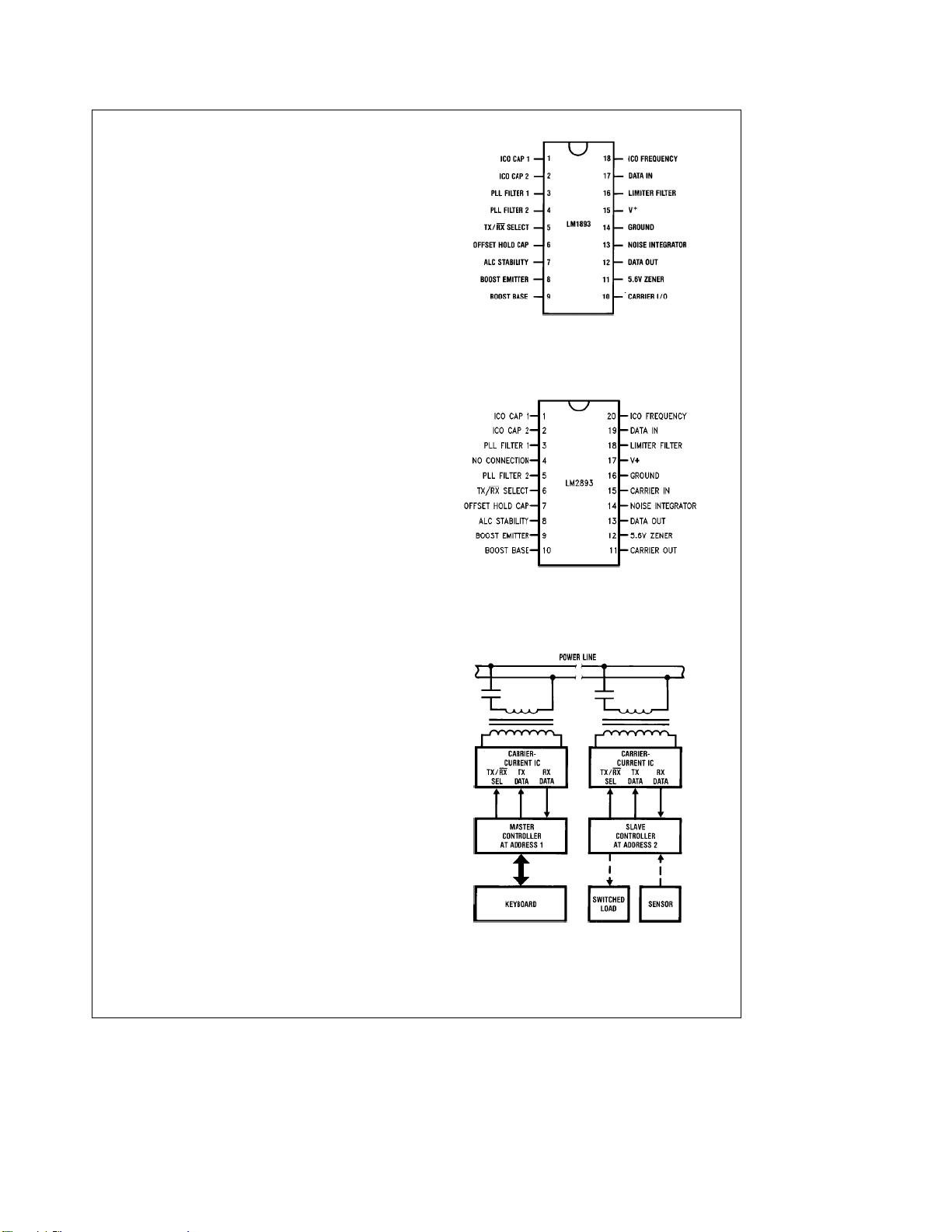
Dual-In-Line Package
Top View
Order Number LM1893N
See NS Package Number N18A
Small Outline & Dual-In-Line Package
Top View
Order Number LM2893M or LM2893N
See NS Package Number M20B or N20A
FIGURE 2. Connection Diagrams
FIGURE 3. The block diagram of a carrier-current
system using the Bi-Line chip to interface digital
controllers via the power line
*Unless otherwise noted, all pin references refer to LM1893, but hold true
for equivalent LM2893 pin.
6
TL/H/6750– 2
TL/H/6750– 41
TL/H/6750– 3
Page 7
Application Information (Continued)
TL/H/6750– 4
FIGURE 4. Block diagram of a CCT system with the boost and 5V supply options shown in dashed boxes
7
Page 8

Application Information (Continued)
Recommended
Ý
Value
Purpose
CO560 pF Together, COand ROIncreases F
R
6.2 kX set ICO FO. Increases F
O
CF0.047 mF PLL loop filter pole Less noise immune, higher More noise immune, lower Depending on RFvalue and
RF3.3 kX PLL loop filter zero PLL less stable, allows PLL more stable, allows CF. See Apps. Info. C
CC0.22 mF Couples FOto line, Low TX line amplitude. Drives lower line Z.
CCand T1low-pass Less 60 Hz T1current. More 60 Hz T1current. on hot and neutral for max.
attenuates 60 Hz. Less stored charge. More stored charge. line isolation, safety.
CQ0.033 mF Tank matches line Z, Tank FOup or increase Tank FOdown or decrease 100 V nonpolar, low TC,g10%
bandpass filters, L of T
T
Use isolates from line, Smaller L: higher FOor Larger L: lower FOor Optimize for low FOline
1
recommended and attenuates increase CC; decreased FOdecrease CC; increased FOpull with control of FOTC
XFMR transients. line pull. line pull. and Q.
CA0.1 mF ALC pole Noise spikes turn ALC off. Slower ALC response. RAoptional. ALC stable
R
10 kX ALC zero Less stable ALC. More stable ALC. for C
A
CL0.047 mF Limiter 50 kHz pole, Higher pole F, more 60 Hz Lower pole F, less 60 Hz Any reasonably low TC cap.
60 Hz rejection. reject. F
CM0.47 mF Holds RX path VOSLess noise immune, shorter More noise immune, longer Low leakageg20% cap.
CI0.047 mF Rejects short pulses Less impulse reject, less More impulse reject, more CIcharge time (/2 bit nom.
like impulse noise. delay, more pulse jitter. delay, less pulse jitter. Must be
RC10 kX Open-col. pull-up Less available sink I. Less available source I. R
RZ12 kX 5.6 V Zener bias Larger shunt current, Smaller shunt current, 1kI
t
Z
44 V BV Transient clamp ZTfailure, higher series ZTcostly, lower series Recommend Zener rated
T
k
60 V peak R-excess peak V, Zener R gives enhanced fort500 W for 1 ms.
R
4.7 X Transient I limit Damage ZT, pull up Va. Excessive TX attenuation. Carbon comp. recommended.
T
t
D
44V BV Over-drive Clamp Failure on Transient Costly IRF 11DQ05 or 1N5819
T
RB180 X Base bleed Faster, lower THD IO. Inadequate turn-off speed. Boost optional. QBF(b3 dB)
Q
Power NPN Boost gain device Excessive TJand V
B
RG1.1 X Current setting R More IO, need higher hfe. Less IO, lower min. hfe.I
t
C
47 mF Supply bypass Transients destroy chip. Less supply spike. Vanever over abs. max.
B
ZA5.1V Stop ALC charge Excess ALC ALC RX charging ZAoptional - 5.1V
in RX mode current flow not inhibited over T
FIGURE 5. A quick explanation of the external component function using the circuit of
18 V, F
e
O
125 kHz, f
Effect of making the component value:
Smaller Larger
O
k
5.6 k not recommended.l7.6 k not recommended. Poor FOTC withk5.6kRO.
f
DATA
O
, more PLL stability. f
Decreases F
Decreases F
DATA
O
O
, less PLL stability. FO, PLL unstable with large
g
5% NPO ceramic. Use low TC
2 k pot and 5.6 k fixed R.
less CF. Less ringing. more CF. More ringing. and RFvalues not critical.
t
250 V non-polar. Use 2C
for constant FO. L of T1for constant FO. High large-signal Q needed.
1
attenuation? reject, more noise BW. 300 pF guarantees stability.
O
VOShold, faster VOSaqui- VOShold, slower VOSaqui- Scale with f
sition, shorter preamble. sition, longer preamble.
t
C
more chip dissipation. less V
a
current draw. (Chip power-up needs 5.6 V)
Notes
t
100 pF.
A
.
DATA
k
1 bit worst-case.
1.5 kX on 5.6 V
k
30 mA recommended.
Z
F
and chip damage, transient clamp,
less ruggedness. more ruggedness.
. More rugged, but costly. ofl200 MHz. R
SAT
e
360 Baud (180 Hz), using a 115 V 60 Hz power line
DATA
J
Figure 4
e
70[(10aRG)/R
O
g
20% low leakage type
. Values given are for V
B
l
24 Ohm.
]
G
mApp.
C
a
e
Component Selection
Assuming the circuit of
er than the nominal 125 kHz carrier frequency, 180 Hz data
rate, 18V supply voltage, etcetera, the component values
listed in
Figure 5
direct the CCT designer in finding the required component
values with emphasis placed on look-up tables and charts. It
is assumed that the designer has selected values for carrier
center frequency, F
power line voltage, V
or more of those parameters is not defined, one may read
the data sheet and make an educated guess.
Maxims to keep in mind, based on CCT electrical perform-
Figure 4
is used with something oth-
will need changing. This section will help
; data rate, f
O
; and power line frequency, FL.Ifone
L
; supply voltage, Va;
DATA
ance considerations only, are: 1) the higher the F
ter, 2) the lower the maximum data rate the better, and 3)
the more time and frequency filtering the better.
Use
Figure 5
as a quick reference to the external compo-
nent function.
THE TRANSMITTER
C
O
Central to chip operation is the low TC of FOemitter-coupled oscillator. With proper C
tude triangle-wave oscillator output may vary from near DC
to above 300 kHz. While C
, the FOof the 2VBEampli-
O
may have any value, COshould
O
8
the bet-
O
Page 9

Component Selection (Continued)
be made above 10 pF so that parasitic capacitance is not
dominant. Excessive or unbalanced common-mode-toground capacitance should be avoided. A low temperature
coefficient (TC) of capacitance (
monolithic NPO ceramic multilayer type, preserves low TC
of F
.
Figure 6
O
R
O
finds a COvalue given FO.
Resistor ROis used by the IC to generate a VBE/R related
current that is multiplied by 2 to produce the 200 mA ICO
control current that sets F
the V
related tri-wave amplitude across COto effect a low
BE
TC of F
. Vary ROto trim FO, within limits. Raising FOmore
O
than 20% above its untrimmed value by means of decreasing R
more than 20% is not recommended. Low RO, and
O
so high control current, risks ICO saturation and poor TC
under worst-case conditions. Raising R
modulated signal amplitude from the phase detector; raising
R
by more than a factor of 2 (1 octave) is not recommended.
O
Since lower TC pots are relatively costly, it is recommended
that R
be made up of a 5.6 k fixed (k100 PPM/§C) resistor
O
and R
k
250 PPM/§C) series pot.
A
witha2kX(
C
A
Components CAand RAcontrol the dynamic characteristics
of the transmitter output envelope. Their values are not critical. Use the values given in
tions of loaded T
noise. Any changes made in C
tank Q, RO,f
1
based on empirical measurements of a CCT on the line.
Roughly, C
acts as an ALC pole and RAan ALC zero.
A
k
100 PPM/§C), such as a
. The control current TC ‘‘bucks’’
O
reduces the de-
O
Figure 5
.CAand RAare func-
, and line impulse
DATA
and RAshould be made
A
T
1
At this point, the CCT system designer may choose to use
one of the recommended transformers or to design custom
T
. Consult ‘‘The Coupling Transformer’’ section to help
1
with the design of T
is needed. The recommended 125 kHz transformer functions with an I
if a new or boost-capable transformer
1
of up to 600 mApp.
O
It is recommended that CCT systems use the recommended
transformers, described in
Figure 7
, for T1. The 3 transformers are optimized for use in the ranges of 50 –100 kHz, 100 –
200 kHz, and 200 – 400 kHz with unloaded Q’s (Q
35, and loaded Q’s (Q
are supplied with nominal 7.07, 10, and 14.1 turns ratios (N)
) of about 12. Three secondary taps
L
) of about
U
to drive industrial and residential power line impedances of
3.5, 7, and 14X respectively. All are inexpensive, all have
the same pin-outs for easy exchange in a PC board, and all
are small - on the order of 10 mm diameter at the base.
C
Q
Tank resonant frequency FQmust be correct to allow passage of transmitter signal to the line. Use
C
’s value. Trimming FQto equal FOis done with T1’s trim-
Q
ming slug. The inductance of T
which may be cancelled by using a
hasaTCofa150 PPM/§C
1
Figure 8
b
150 PPM/§C cap such
to find
as polystyrene. Since circulating current in the tank is (/4
A
resistance is too much). Polypropelene caps are excellent,
should have a low series resistance (a 1 X series
RMS,CQ
‘‘orange drop’’ mylars are adequate, while many other mylars are inadequate. A 100V rating is needed for transient
protection.
FIGURE 6. Find CO’s value knowing F
Bottom View
TL/H/6750– 6
125 kHz
Toko 707VX-A042YUK
FIGURE 7. The recommended T1transformers, available through:
Toko America, 1250 Feehanville Drive, Mount Prospect, IL, 60056, (312) 297-0070
TL/H/6750– 5
O
TL/H/6750– 7
50 kHz
Toko 707VX-A043YUK
9
FIGURE 8. Find CO’s value given F
TL/H/6750– 8
300 kHz
Toko 161XN-A207YUK
TL/H/6750– 10
O
TL/H/6750– 9
Page 10

Component Selection (Continued)
C
C
Capacitor CC’s primary function is to block the power line
voltage from T
side winding comprise a LC highpass filter. The self-inductance of T
C
must have a low enough impedance at FOto allow T1to
C
drive transmitted energy onto the line. To drive a 14X power
line, the impedance of C
Use
Figure 9
that it is less than the line impedance. Then check
to see that the power line current is small enough to keep
T
well out of saturation; the recommended transformers
1
can withstand a 10 Amp-turn magnetizing force (1 Amp
through the worst-case 10 turn line-side winding).
Caution is required when choosing C
nance of the series combination of C
ductance, and the reflected tank impedance. The low resistance of the network under series resonance will load the
line, possibly decreasing range. For your particular line coupling circuit, measure for series resonance using some expected line impedance load.
R
B
This base-bleed resistor turns QBoff quickly - important
since the amplifier output swing is about 200V/ms. An R
below about 24X will conduct excessive current and overload the chip amplifier and is not recommended.
’s line-side winding. Also, CCand T1’s line-
1
is far too low to support a direct line connection.
1
should be below 14X.
C
to find the reactive impedance of CCto check
Figure 10
to avoid series reso-
C
, the transformer in-
C
neous power of greater than 1 kW has been measured using the recommended transformers). For self protection, the
Carrier I/O has an internal 44V voltage clamp with a 20X
series resistance. A parallel low impedance 44V external
transient suppression diode will then conduct the lion’s
share of any current when transients force the Carrier I/O to
a high voltage.
FIGURE 10. The AC line-induced current passed by C
B
TL/H/6750– 12
C
FIGURE 9. CC’s impedance should be,
TL/H/6750– 11
as a rule-of-thumb, smaller than the lowest
expected line impedance
R
G
This resistor, in parallel with the internal 10X resistor, fixes
the current gain of the output amplifier, and so the output
current amplitude.
mum AC current gain h
output current.
Q
B
Figure 11
gives output current and mini-
for QBwhen RGis used to boost
fe
The boost gain transistor QBmust be fast. Double-diffused
devices with 50 MHz F
types) do not preserve a sinusoidal waveform when F
high or will cause the output amp. to oscillate. Q
a certain minimum h
Figure 11.Figure 12
continuously operating with a shorted output. BV
RB) must be 60V or greater and QBmust have adequate
’s work, slower transistors (epi-base
T
must have
for given boost levels, as shown in
fe
shows the power QBmust dissipate
B
(R
CER
O
SOA for transient survival.
Z
T
Unfortunately, potentially damaging transient energy passes
through transformer T
onto the Carrier I/O pin (instanta-
1
FIGURE 11. Output amplifier current and required min.
TL/H/6750– 13
Q
versus gain-setting resistor R
Bhfe
G
TL/H/6750– 14
FIGURE 12. Boost transistor power dissipation versus
amplifier output current
Z
must be used unless some precaution is taken to protect
T
the Carrier I/O pin from line transients or transients caused
when stored line energy in C
phase of power line connection and disconnection. Worst
case, C
is
may discharge a full peak-to-peak line voltage into
C
the tuned circuit. Another way to reduce the need for Z
by placing another magnetic circuit in the signal path that
e
relies on a high, but easily saturated, permeability to couple
a primary and secondary winding - a toroidal transformer for
example. Toroids cost more than Z
is discharged by the random
C
.
T
is
T
Use an avalanche diode designed specifically for transient
suppression Ð they have orders of magnitude higher pulse
10
Page 11

Component Selection (Continued)
power capability than standard avalanche diodes rated for
equal DC dissipation. Metal oxide varistors have not proven
useful because of their inferior clamping coefficient and are
not recommended. Specifications for an example minimum
diode are given in
Breakdown Voltage 44 –49V@1mA
Maximum Leakage 1mA@40V
Capacitance 300 pF@BV
Maximum Clamp Voltage 64.5V@7.8A
Peak Non-Repetitive Pulse Power 10 kW for 1 ms
(REA Standard Exponential Pulse)
Surge Current 70A for 1/120s
FIGURE 13. Key specifications for a recommended
transient suppressor Z
Semiconductor, 2001 West Tenth Place, Tempe, AZ
R
T
RTacts as a voltage divider with ZT, absorbing transient
energy that attempts to pull the Carrier Input pin above 44V.
Make the resistor a carbon composition 1/4W. When experiments discharging C
AC thru a 1X power line were carried out, film resistors blew
open-circuit.
D
T
This Schottky diode is placed in parallel with the CCT chip’s
substrate diode to pass the majority of the current drawn
from ground when the Carrier Input or Carrier Output is
pulled below ground by a larger-than-twice-the supply-swing
on the tank. Note that Z
diode, but is ineffective due to its high forward voltage drop
and high diffusion capacitance caused by its low forward
speed. Tests proved that a 1N5818 kept a receive-path
functional with a 20X boost transmitter with a 7:1 transformer attempted to swing the receiver’s Carrier I/O to
(300 mA peak ground current in the receiver). Without D
the receiver momentarily stops functioning at a 100 times
lower ground current.
This diode is not needed if the Carrier I/O never swings
below ground. If your CCT systems all run on the same
regulated voltage with all matched transformers and turns
ratios, it is not needed. Otherwise, it is.
THE RECEIVER
The receiver and transmitter share components C
R
T,ZT,CO,RO
that are not in need of change for RX mode operation. Values for the balance of the components are now found.
Line-Frequency Rejection
To use the ultimate sensitivity of the device, fully 110 dB of
115 V, 60 Hz attenuation is required between the line and
the limiter amplifier output. Using the circuit topology of
ure 4
, the combined attenuation of the CC/T1highpass, the
tuned transformer, and the bandpass filter attenuation of
the limiter amplifier give far more line rejection than the
above-stated minimum. However, if some other CCT line
coupling circuit is used, line rejection will become important
to the system designer.
Receiver input power supply rejection (PSRR) and commonmode rejection (CMRR) are one-in-the-same using the supply-referenced signal input of
Figure 13
.
available from General
T
85281, 602–968-3101, part no. SA40A
charged to the peak-to-peak 620V
C
is in parallel with the substrate
T
, and peripheral supply and bias components
Figure 4
. Ripple swings both
g
100V
C,T1,CQ
Fig-
differential inputs of the Norton amp. equally, while the single-ended input signal swings only the positive input. Overall
PSRR consists of the input CMRR (set by the input stage
component matching) and the ripple-frequency attenuation
of the input amplifier bandpass response that passes carrier
frequency but stops low frequencies. A typical 1% resistor
and 1 mV n-p-n mirror offsets give 26 dB of attenuation, the
bandpass gives 54 dB 120 Hz attenuation, for an overall 80
dB PSRR to allow tens of volts of ripple before impacting
ultimate sensitivity.
C
C
A value was chosen earlier. Knowing T1’s secondary inductance allows a check of LC line attenuation using
C
L
The Norton input limiter amplifier has a bandpass filter for
enhanced receiver selectivity, noise immunity, and line frequency rejection. The nominal response curve for F
kHz is shown in
kHz pole is set by C
line frequency attenuation is found for the bandpass filter.
Use
Figure 15
Figure 15
. The 300 kHz pole is fixed. The 50
’s value. After CLis found, the resulting
L
to find a CLvalue given for FO. The approximate line frequency attenuation of the bandpass filter may
then be found in
Figure 16.Figure 15
33% larger than nominal, giving a low frequency pole 33%
low to allow for component tolerances.
,
T
FIGURE 14. The 60 Hz line rejection of the highpass
filter made up of C
(neglecting capacitive coupling)
and T1’s line-side winding
C
,
FIGURE 15. Given FO,CLis found. Also shown is the
input amplifier’s small signal amplitude response
Figure 14
e
O
returns a value for C
TL/H/6750– 15
TL/H/6750– 16
TL/H/6750– 17
.
50
L
11
Page 12

Component Selection (Continued)
C
and R
F
F
These phase-locked loop (PLL) loop filter components remove some of the noise and most of the 2F
present in the demodulated differential output voltage signal
from the phase detector. They affect the PLL capture range,
loop bandwidth, damping, and capture time. Because the
PLL has an inherent loop pole due to the integrator action of
the ICO (via C
R
gives the loop filter a classical 2nd-order response.
F
), the loop pole set by CFand the zero set by
O
FIGURE 16. The Norton-input limiter amplifier bandpass
filter line-frequency signal attenuation given C
FIGURE 17. Find CFgiven FO.
gives the maximum data rate
and RFgive the most stable PLL with the fastest
No C
F
response. Large C
instability leading to poor capture range and poor step re-
’s with a too-small RFcause PLL loop
F
sponse or oscillation.
Calculation of C
the 2nd-order loop step response, but also the PLL non-
and RFis quite difficult, involving not only
F
dominant poles, the tuned transformer stepped-frequency
response, and the RC lowpass step response (for data rates
approaching 1 kHz). C
pirically. Tolerance is not critical. Component values are se-
and RFvalues are best found em-
F
lected to give the best possible impulse noise rejection
while preserving a
margin.
Figures 17
where ‘‘f
DATA
should be less than the maximum data rate, in kHz, from
Figure 19
Note that C
data rates and are not plotted against data rate - as one
g
20% capture range and wide stability
and18give CFand RFvalues versus FO,
kk
MAX DATA RATE’’ means that f
divided by 10.
and RFare a function of data rate only for high
F
might expect. The reason for this is important to understand
if the CCT system designer wishes to find C
cally. Data signal is, loosely speaking, passed through the
PLL loop and is therefore potentially attenuated if the loop
bandwidth is on the order of the 3rd harmonic of the data
rate, or less. Overall loop bandwidth is held as low as possible for maximum noise rejection while passing the data.
Loop bandwidth is roughly proportional to the geometric
mean of the unfiltered loop bandwidth and the filter pole set
by C
. Therefore, CFis related to data rate. Unfortunately,
F
the loop capture range falls to critically low values when
large enough values of C
width down to the 100’s of Hz range, for low data rates. The
are used to reduce loop band-
F
components
O
TL/H/6750– 18
TL/H/6750– 19
Figure 19
and RFempiri-
F
L
DATA
obvious way out is to then reduce the unfiltered loop bandwidth. That bandwidth is approximately proportional to the
value of C
tion requires a larger C
chip, changing the control current is not allowed. So one is
forced to choose a C
capture range, say
. For a fixed FO, unfiltered loop bandwidth reduc-
O
and larger control current. With this
O
combination with some minimum
F/RF
g
20%, that is within some guardband
from the point of loop instability. Happily, impulse noise
tends to last only fractions of a millisecond so that the lack
of low bandwidth loop response with low data rates is not a
heavy penalty. As long as there is adequate capture range,
the impulse noise filter performs admirably. Note that reducing F
will reduce the no-filter loop bandwidth, and indeed
O
the maximum data rate falls below the limit set by the RC
lowpass filter as F
The tuned transformer characteristics will affect the demodulated data waveform more than C
rates. Tank Q and off-tuning will affect overshoot during the
falls below 100 kHz (
O
Figure 19
and RFat low data
F
FSK frequency steps. This is a property of tuned circuits.
The maximum data rate of
Figure 19
is measured from the
receiver input to the Data Out and does not include the data
bandwidth reducing effects of T
C
M
.
I
Capacitor CMstores a voltage corresponding to a correction
factor required to cancel the phase detector differential output DC offsets. The stored voltage is ±/6 of the DC offset
plus some bias level of about 2.2 V. A large C
creases the time required to bias-up the receive path at the
beginning of transmission. A large C
store its bias voltage long. Because of the initial random
charge of C
charge to the proper bias voltage. Therefore, reducing C
, the receiver must be given a data transition to
M
does filter well and
M
value to one that may be charged in less than 2 bit-times will
not save biasing time and is not recommended.
FIGURE 18. Find RFgiven FOwith F
DATA
a parameter
FIGURE 19. The maximum data rate versus FOusing
loop filter components optimized for max. noise
performance while retaining a min.
g
20% capture
range (large signal)
Use
Figure 20
the standard 2 bit receive charge time is desired. The cap.
to find CM’s value knowing f
DATA
value and TC are not critical, but the capacitor should have
low leakage.
12
).
value in-
M
M
TL/H/6750– 20
TL/H/6750– 21
, assuming
’s
Page 13

Component Selection (Continued)
FIGURE 20. Size CMassuming a 2 bit-time
receive bias time
C
I
The impulse noise filter integrator capacitor CIis used to
disallow the passage of any pulse shorter than the integrator charge time. That charge time, set to a nominal (/2 bit
time, is the time required for a
swing C
overa2VBErange. Charge time under worst case
I
conditions must never be greater than a bit time since no
signal could then pass. Using a
g
50 mA charge current to
g
10% capacitor, full junction temperature range, and full specified current range, a
maximum nominal charge time of (/2 bit is recommended.
Figure 21
R
gives CIversus data rate under those conditions.
C
The collector pull-up resistor is sized to supply adequate
pull-up current drive and speed while preserving adequate
output low current drive.
TL/H/6750– 22
Z
A
The 5.1V silicon zener diode ZAis required when a short
RX-to-TX switch-over time is needed at the same time that
the chip is operating in the RX mode with a pin 10 input
signal swing approaching or exceeding twice the supply
voltage. Predominant causes of these large swings impinging on the RX input are: 1) a transmitter’s supply voltage
higher than the receiver’s supply voltage, 2) a TX and RX
pair that are electrically close, or, 3) a higher RX T
turns ratio than the TX T
step-down ratio.
1
step-up
1
Normally, when in the RX mode with small incoming signal
on pin 10, the ALC remains off with pin 7 at a 6V
b
(V
2VBE) bias voltage. CAis then charged to 6V. TX
Z
mode may then be selected with 6V on C
TX power to pump T
quickly for fast RX-to-TX switch time. As TX output swing
’s tuned circuit, and so the AC line,
1
increases so that pin 10 swings below V
that ALC activates to charge C
output drive. However, if in the RX mode pin 10 ever swings
below V
TX mode is selected with C
will charge to above 6.6V. Now, when the
ALC,CA
100% TX output drive is available to pump T
to about 6.6V to reduce TX
A
at 6.6V, somewhere from 0 to
A
resulting in a slower rising line signal - effectively reducing
allowing 100%
A
(4.7V typically),
ALC
’s tuned circuit
1
the RX-to-TX switch time.
Use a 5.1V Z
guarantee over-temp. operation. R
Z
to limit current flow and should never fall below 1 kX.If
A
R
is less than 1 kX, then puta2kXresistor in series with
A
Z
. Logic high voltages above 10V will cause current flow
A
into pin 7 that must be limited to 1 mA (with R
series R).
driven bya0to0.8V logic low signal to
A
must be in series with
A
or a
A
Breadboarding Tips
During CCT system evaluation, some techniques listed below will simplify certain measurements.
Ð Use caution when working on this circuit - dangerous
line voltages may be present.
Ð When evaluating PLL operation, offset cancel circuit op-
eration, and loop filter values, use the filter of
FIGURE 21. Impulse noise filter cap. CIversus F
where the charge time is (/2 bit time
TL/H/6750– 24
DATA
FIGURE 22. Circuit to view the differential demodulated data signal, minus the noise and 2FOcomponents,
conveniently with a single-ended gain-of-one output
to view the demodulated signal minus the 2FOand noise
components. This filter models the RC lowpass filter on
chip.
13
Figure 22
TL/H/6750– 25
Page 14

Breadboarding Tips (Continued)
Ð When evaluating CCT system noise performance on a
real power line, it is desirable to vary the signal amplitude to the receiver. This is not easy. An in-line lineproof L-pad is fine except that the line impedance is unknown and variable and so the L-pad will rarely match.
Instead, the power output of a chip transmitter may be
controlled using the circuit of
Figure 23
. This circuit con-
trols the ALC.
Ð It is sometimes desirable to place impulse noise on the
line. A simple light dimmer with a 100 W light bulb load
produces representative impulse noise.
Ð Do not allow peak currents of over 1 A through the 5.6 V
Zener. In other words, don’t short charged capacitors
into this low-impedance device. Take care not to momentarily short pins 10 and 11 - chip damage may result.
Ð
Figure 24
shows some typical signals beginning with se-
rial data transmitted to received signal.
Tuning Procedure
This procedure applies to circuits similar to
or LM2893 circuit.
First, trim F
logical high data input, and measuring the TX high frequency, 1.022 F
by putting the chip in the TX mode, setting a
O
, on the Carrier I/O using these steps:
O
1. Take pin 17 to a logic low.
2. Take pin 5 to a logic high.
3. Place a counter on pin 10.
4. Adjust R
on pin 18 for Fe1.022FO.
O
Second, the line transformer is tuned. The chip is placed in
the TX mode, a resistive line load is connected to disable
the ALC by reducing tank voltage swing below its limit. FSK
data is then passed through the tank so that the tank envelope may be adjusted for equal amplitude for high and low
data frequency.
1. Take pin 5 to a logic high.
2. Place a logic-level square wave at or below the receiver’s
maximum data rate on pin 17.
3. Temporarily place a 330 X resistor across the tank.
4. Place a scope on pin 10.
5. Adjust the transformer slug for the least envelope modulation.
In lieu of the 330 X resistive load, T
power line to better simulate actual load and tank pull conditions during tank tuning. Alternatively, a passive network
Figure 4
LM1893
may be coupled to the
1
representing an average line impedance may be connected
to the line side of T
used to defeat the leveling effect of the ALC.
. The circuit of
1
Figure 23
should then be
TL/H/6750– 26
FIGURE 23. A means of transmitter output amplitude
control is shown
Thermal Considerations
It is desirable to place the largest possible signal on the
power line for maximum range, limited only by the chip power dissipation and maximum junction temperature T
falling output power at elevated T
power output - high power at low T
T
for chip self-protection. However, it is still possible to
J
exceed the maximum T
perature limit (T
100% TX duty cyle, high supply, shorted load, poor PC
within the specified ambient tem-
J
e
85§C) under worst case conditions of
A
allows a more optimal
J
and lower power at high
J
board layout (with small copper foil area), and an above
nominal current part. Under those conditions, a part may
dissipate 2140 mW, reaching a T
mittedly a rare occurrence). Proper system design includes
the measurement or calculation of T
function under worst-case operation. Like all devices with
e
170§C worst-case (ad-
J
max. to guarantee
J
failure modes modeled by the Arrhenius model, the high
chip reliability is further enhanced by keeping the die temperature mercifully below the absolute maximum rating.
A direct method of measuring operating junction temperature is to measure the V
ways available under all operating modes. The graph of
ure 25
may be used to find TJ, knowing VBEat the operating
point in question and V
by powering up a chip (in RX mode) that has been dissipating zero power at some T
V
in less than 1 s (for better than 5§C accuracy).
BE
voltage on pin 18, which is al-
BE
e
at T
BE
A
e
T
A
25§C. VBEis found
J
for some time and measuring
Alternately, TJmay be calculated using:
e
a
T
T
J
iJAP
A
D
where iJAis 75§C/W for the plastic (N) package using a
socket. That i
value is for a high confidence level; nomi-
JA
. The
J
Fig-
(1)
TL/H/6750– 23
FIGURE 24. Oscillogram revealing signals at several important nodes under weak signal (0.5 mV
SCR spikes on an otherwise quiet 115 V, 60 Hz power line. The signals are: 1) transmitted data, 2) RX carrier on the
tuned transformer, 3) demodulated signal from the PLL after passing thru circuit of
Figure 22
) conditions with
RMS
, 4) signal after RC
lowpass, 5) data at impulse noise filter integrator, and 6) received data. Horizontal scale is 10 ms per div.
14
Page 15

Thermal Considerations (Continued)
for an N package is 60§C/W, lower with good PC
nal i
JA
board layout. Since P
an iterative solution process starting with an initial guess for
T
is used. With the estimated TJ, find the total supply cur-
J
rent found in the typical performance characteristics.
FIGURE 25. TJmay be found by using the temperature
coefficient of pin 18 V
is a relatively strong function of TJ,
D
TL/H/6750– 27
if VBEis known at 25§C
BE
Transmit-To-Receive
Switch-Over Time
An important figure-of-merit for a half-duplex CCT link, affecting effective data rate, is the TX-to-RX switch time T
Using the recommended component values gives this part a
nominal 2 bit-time (1 bit time
range of operating conditions, where the receiver requires 1
data transition. T
does increase as noise filtering, especially via C
creased. Impulse noise at switch, signals near the limiting
sensitivity, poor F
because of poor trim or worst-case conditions, and the statistical nature of PLL signal acquisition may all contribute to
increase T
T
The receiver was designed to ‘‘remember’’ the RX-mode
DC operating points on C
Under noisy worst case conditions, C
point of false operation after 35 bit-times in the TX mode
(1400 bit times with no noise and a nominal part, f
180 Hz). TTRis about 0.8 ms (proportional to the selected
F
The major components of T
nominal 125 kHz F
a Q of 20, and the circuit of
been operating in the TX mode with a 26.6 V
and is now selected as a receiver. An incoming signal requiring the ultimate receiver sensitivity immediately is placed
on the line.
First, the tank stored energy at the transmit frequency must
decay to a level below the 2.8 mV
0.14 mV
to be received.
decay time
q
That is 0.47 ms of delay (proportional to I/F
Second, the PLL must acquire the signal; it must lock and
settle. Acquisition time is statistical and may take any length
of time, but average acquisition time depends on the loop
filter components C
frequencies, DF
TR
is lower when a pair of LM1893’s handshake rapidly.
TR
) plus (/2 bit-time.
O
RMS
20
c
125 000
cannot be decreased significantly but
TR
match between receiver and transmitter
O
to possibly 4 bit-times.
, 180 Hz f
O
incoming line signal containing the information
Q
e
ln
qF
O
26.6
ln
0.0028
#
F
, of the TX/RX pair. Using the recom-
O
e
1/[2f
and CFwhile in the TX mode.
M
are described below for a
TR
DATA
Figure 4
V
1
e
V
#
J
O
e
0.466 ms (2)
J
and RFand the difference in center
]
) over a wide
DATA
will discharge to the
M
, lightly-loaded tank with
. The remote CCT has
PP
swing caused by the
PP
and Q).
O
TR
,isin-
M
DATA
tank swing
mended C
(ag100 mV DC offset on CFand RF), lock was measured
to take less than 50 cycles of F
(proportional to 1/F
Acquisition is incomplete until the second order PLL loop
settles. For the above-mentioned C
ral frequency F
2.3 kHz and 1.0 respectively. Settling to within
the
or 1.2 ms (a function of C
Third, the RC lowpass filter introduces a 0.12 ms delay.
Fourth, C
ing on the polarity of F
noise immunity is possible with only
ing. C
mated by assuming a 50 mA charge current and the full 83
mV charge voltage. C
tional to 1/f
Fifth, the impulse noise filter adds a (/2 bit-time delay. Total
T
TR
360 Baud.
and RF(47 nF and 6.2 kX) with ag4.4% D F
F
. That is a 0.40 ms delay
).
O
and damping factor are found to be
N
g
100 mV DC offset change requires 2.7 periods of FN,
must charge up tog(±/6)100e83 mV depend-
M
charge current is an asymptotic function approxi-
M
DATA
is 3.9 ms plus (/2 bit-time for a total of 1.9 bit-times at
O
M
).
O
and RF, the loop natu-
F
g
25 mV of
and RF).
F
. Borderline data squaring with zero
charge time is then 1.7 ms (propor-
g
(±/6) 50 mV of charg-
O
Receive-To-Transmit
Switch-Over Time
.
Assume the chip has been in the RX mode and the TX
mode is now selected. In less than 10 ms, full output current
is exponentially building tank swing. 50% of full swing is
achieved in less than 10 cycles - or under 80 ms at 125 kHz.
In the same 10 ms that the output amp went on, the phase
detector and loop filter are disconnected and the modulator
input is enabled. FSK modulation is produced in 10 ms after
switching to TX mode.
Power Line Impedance
Irrespective of how wide the limits on power line impedance
Z
are placed, there are no guarantees. However, since the
L
CCT design requires an estimate of the lowest expected line
impedance Z
ter-to-line coupling, line impedance should be measured
and Z
e
L
values for T
quency pull F
sign that functions with the overwhelming majority of power
lines.
A limited sampling of Z
sign, of residential and commercial 115V 60 Hz power line.
Data was also drawn from the research of Nicholson and
Malack (reference 1), among others, to produce
and27. All measured impedances are contained within the
shaded portions of
Z
is used throughout the application information with a
LN
nominal 45
ty).
FIGURE 26. Measured line impedance range for
residential and commercial 115V, 60 Hz lines
encountered for the most efficient transmit-
LN
limits fixed to a given confidence level. Reasonable
turns ratio, loaded Q, and tank resonant fre-
1
may be found to enable a CCT system de-
Q
was made, during the LM1893 de-
L
Figures 26
Figure 27
phase angle (0§is sometimes used for simplici-
§
. A nominal 3.5, 7.0 and 14 X
TL/H/6750– 28
15
Page 16

Power Line Impedance (Continued)
FIGURE 27. Complex-plane plots of measured 115V, 60 Hz line impedance where Z
TL/H/6750– 29 TL/H/6750 –30
Power Line Attenuation
The wiring in most US buildings is a flat 3 conductor cable
called Amerflex, BX, or Romex. All referenced line impedances refer to hot-to-neutral impedances with a grounded
center conductor. The cable has a 100 X characteristic impedance, a 125 kHz quarter-wavelength of 600 m (250 m at
300 kHz), and a measured 7 dB attenuation for a 50 m run
with a 10 X termination. Generally, line loads may be treated as lumped impedances. Instrument line cords exhibit
about 0.7 mH and 30 pF per meter.
Limited tests of CCT link range using this chip show extensive coverage while remaining on one phase of a distribution transformer (100’s of m), with link failure often occuring
across transformer phases or through transformers unless
coupling networks are utilized. Total line attenuation allowed
from full signal to limiting sensitivity is more than 70 dB.
Typically, signal is coupled across transformer phases by
parasitic winding capacitance, typically giving 40 dB attenuation between phased 115 V windings. Coupling capacitors
may be installed for improved link operation across phases.
Power factor correcting capacitor banks on industrial lines
or filter capacitors across the power lines of some electronic
gear short carrier signal and should be isolated with inductors. Increasing range is sometimes accomplished by electing to install the isolating inductors (
capacitors, as well as by electing to use the boost option.
Frequency translating or time division multiplexed repeaters
will also increase range.
FIGURE 28. An isolation network to prevent: 1) noise
from some device from polluting the AC line, and 2) to
stop some low impedance device (measured at F
from shorting carrier signal. Component values given
as an example for F
residential power lines
Figure 28
e
125 kHz on
o
) and coupling
TL/H/6750– 40
)
o
The Coupling Transformer
The design arrived at for T1is the result of an unhappy
compromise - but a workable one. The goals of 1) building
a
jX
L
e
e
Q
TL/H/6750– 31
L
, and of
L
likely
L
7.07, 10, and
e
35).
U
FOand some
,is
1
(3)
(4)
e
R
L
T
with a stable resonant frequency, FQ, that is little affect-
1
ed by the de-tuning effect of the line impedance Z
2) building a tightly line-coupled transformer for transmitted
carrier with loose coupling for transients, are somewhat mutually exclusive. The tradeoffs are exposed in the following
example for the CCT designer attempting a new boost-capable, or different core, transformer design.
The compromises are eased by separating the TX output
and RX input in the LM2893. An untuned TX coupling transformer with only core coupling (not air-coupled solenoid
windings) would employ a high permeability, high magnetic
field, low loss, square saturating, toroidal core. The resonant RX path would be isolated from line-pull problems by a
unilateral amplifier that operates at line voltages with much
more than 110 dB of dynamic range, or by a capacitively
coupled pulse transformer driving a unilateral amplifier and
filter, for increased selectivity. See the LM2893-specific applications section.
For a LM1893-style transformer application, first, choose
the turns ratio N based on an estimated lowest Z
encountered, Z
fects line signal. N should be as large as possible to drive
Z
with full signal. If T1has an unloaded Q, QU, of well less
LN
than 35, a guess of N somewhat high should be used and
later checked for accuracy. The recommended transformers
have secondary taps giving a choice of N
14.1 (nominally) for driving Z
spectively (at T
The resonating inductance of the tuned primary, L
sought. Note that, while standard transformer design gives a
transformer self-inductance with an impedance at operating
frequency well above load impedance, the tuned transformer requires a low L
Result: relatively poor mutual coupling.
e
L
1
2qFOQ
It is known that resonant frequency F
minimum bandwidth, or maximum Q, will be required to pass
signal under full load conditions.
R
Q
e
L
1
2q FOQ
Z
is the reflected ZLN,QLis the loaded Q, and parallel
Ê
l
l
LN
resistance R
R
Z
ll l
Q
LN
.
Figure 29
LN
e
25§C, Vae18V, and Q
J
for adequate QUand minimum line pull.
1
R
Z
Ê
ll l
l
LN
L
models all transformer losses and sets QO.
Q
is found knowing that it absorbs full rated power.
Ê
l
shows graphically how N af-
’s of 14, 7.0, and 3.5 X re-
LN
16
Page 17

The Coupling Transformer (Continued)
FIGURE 29. Impressed line voltage for a given Z
e
P
O
where I
e
P
O
R
ll l
Q
is found using ZLNand the value for N found when as-
R
Q
suming Q
Z
l
LN
e
R
Q
R
QS
Only Q
b
the
e
Q
L
An iterative solution is forced where line pull, DFQ, must be
guessed to find Q
pull guess; a large error requires a new guess. Try a BW of
8.7% - that is 4.4% for deviation, 1% for TC of F
3.3% for DF
e
L
1
Knowing the core inductance per turn, L, and L
ber of turns is found.
e
T
1
T is normally an integer, but these transformers require so
few turns that half-turns are specified, remembering that the
remaining (/2 turn is completed on the P.C. board and is
loosely coupled. The secondary turns are calculated
e
T
2
giving an L
kHz transformer mirrors these specifications. The resonating capacitor is
e
C
Q
for each of the 3 taps available
on the recommended transformers
I
OPP
e
IOV
O
202
Ð
is in amps peak-to-peak at an elevated T
O
(18b4.7) 0.06
4
2
V
O
e
Z
Ê
l
LN
P
O
e
35.
U
e
Ê
l
R
e
L
3 dB (half-power) bandwidth by
BW (% of FO)
2qc125 000c11.5
0
T
N
(2qFQ)2L
e
N2Z
LN
1
1
b
Z
Ê
ll l
l
Q
LN
R
Q
e
2
1aQ
U
remains to be found to calculate L1.QLis related to
1
L
- giving Q
Q
442
L
49.0 mH
1
e
L
20 nH/T
0
49.5
1
e
e
7.07
of 0.98 mH. Note that the recommended 125
2
1
1
a
2(bV
e
(7.07)213.9e695 X (8)
1a35
and L1.L1is then used to check the line
7.00e7 turns (15)
e
Va)
ALC
202
e
0.200 W (6)
(bV
ALC
e
1
Z
Ê
l
l
LN
1210
2
e
L
e
49 (/2 turns (13)
33.1c10
(b4.7aVa)I
e
(
a
Va)02
I
O
1
1
1
b
442
695
e
1 X (10)
11.5.
e
49.0 mH (12)
b
9
e
33 nF (16)
TL/H/6750– 32
O
4
J
e
442 X (7)
e
1210 X (9)
, the num-
1
O
L
(5)
(11)
, and
Line pull DF
tude of 14X and up with any phase angle from
DF
Q
(11), an 11.8% bandwidth is required, forcing L
duced to reduce Q. That fix was not implemented; some
signal attenuation under worst-case drift and DF
lowed. L
conducts a (/4 A
was calculated (reference 3) for a ZLmagni-
Q
was 6.4% - well above the 3.3% estimate. Referring to
is already so small that the 31 gauge winding
1
circulating current.
RMS
b
90§to 90§.
to be re-
1
Q
is al-
Line Carrier Detection
While the addition of a carrier detection circuit (for a mute or
squelch function) will only decrease receiver ultimate sensitivity, there is sometimes good reason to employ it to free
the controller from watching for RX signal when no carrier is
incoming, or to employ it to reduce the probability of line
collisions (when multiple transmitters operate simultaneously to cause one or more transmissions to fail). Unless the
detector is heavily filtered or uses a high carrier amplitude
threshold, there will be false outputs that force the controller
to have Data Out data checking capability just as is required
when using no carrier detector. If false triggering is minimized, the probability of line collisions is increased due to
the inability to sense low carrier amplitudes and because of
sense delay. The property of the LM1893 to change output
state infrequently (although the polarity is undefined) when
in the RX mode, with no incoming carrier, reduces the desire
to implement carrier detection and preserves the full ultimate sensitivity. Also, many impulse-noise insensitive transmission schemes, like handshaking, are easily modified to
recover from line collisions.
Regarding this, it should be stated that for very complicated
industrial systems with long signal runs and high line noise
levels, it is probably wise to use a protocol which is inherently collision free so that no carrier detect hardware or software is needed. A token passing protocol is an example of
such a system.
Figure 30
cuit.
shows a low cost carrier amplitude detection cir-
Audio Transmission
The LM1893 is designed to allow analog data transmission
and reception. Base-band audio-bandwidth signals FM
modulate the carrier passing through the tuned transformer
(placing a limit on the usable percent modulation) onto the
power line to be linearly demodulated by the receiver PLL.
Because the receiver data path beyond the phase detector
will pass only digital signal, external audio filtering and amplification is required.
mitter and receiver circuit utilizing a carrier detection mute
circuit. A single LM339 quad. comparator may be used to
build the carrier detect and mute. Filter bandwidth is held to
a minimum to minimize noise, especially line-related correlated noise.
Figure 31
shows a simple audio trans-
Communication and System
Protocols
The development of communication and system protocols
has historically been the single most time consuming element in design of carrier current systems. The protocols are
defined as the following:
1.
Communication protocol
and decoding data that remains constant for every transmis-
: a software method of encoding
17
Page 18

FIGURE 30. A simple carrier amplitude detector with output low when carrier is detected
TL/H/6750– 33
FIGURE 31. A simple linear analog audio transmitter and receiver are shown.
The carrier and 1.6V inputs are derived from the carrier detector of
The remaining 2 LM339 comparators may be used to build the carrier detector circuit.
Communication and System
Protocols
sion in a system. Its first purpose is to put data in a baseband digital form that is more easily recognized as a real
message at the receive end. Secondly, it incorporates encoding techniques to ensure that noise induced errors do
not easily occur; and when they do, they can always be
detected. Lastly, the software algorithms that are used on
the receive end to decode incoming data prevent the reception of noise induced ‘‘phantom’’ messages, and insure the
recovery of real messages from an incoming bit stream that
has been altered by noise.
2.
System protocol
ordinated between nodes in a system. Its first purpose is to
(Continued)
: the manner in which messages are co-
TL/H/6750– 34
Figure 30
ensure message retransmission to correct errors (handshake). Secondly it coordinates messages for maximum utilization and efficiency on the network. Lastly, it ensures that
messages do not collide on the network. Common system
protocols include master-slave, carrier detect multiple access, and token passing. Token passing and master slave
have been found to be the most useful since they are inherently collision free.
Both protocols usually reside as software in a single microcontroller that is connected to the LM1893/2893 I/O. In any
case, some sort of intelligence is needed to process incoming and outgoing messages. UARTs have no usefulness in
18
.
Page 19

Communication and System
Protocols
carrier current applications since they do not have the intelligence needed to distinguish between real messages and
noise induced phantoms.
The difficulty in designing special protocols arises out of the
special nature of the AC line, an environment laden with the
worst imaginable noise conditions. The relatively low data
rates possible over the AC line (typically less than 9600
baud) make it even more imperative that systems utilize the
most sophisticated means available to ensure network efficiency.
With these facts in mind, the designer is referred to a publication intended to aid in the development of carrier current
systems. This is literature
rent Networking System, a 200 pp. book that functions as
the ‘‘bible’’ of Bi-Line system design. It has sections on
LM1893 circuit optimization, protocol design, evaluation kit
usage, critical component selection, and the Datachecker/
DTS case study.
(Continued)
Ý
570075 The Bi-Line Carrier Cur-
Basic Data Encoding (please refer to the pre-
viously mentioned publications for advanced techniques)
At the beginning of a received transmission, the first 0 to 2
bits may be lost while the chip’s receiver settles to the DC
bias point required for the given transmitter/receiver pair
carrier frequency offset. With proper data encoding,
dropped start bits can be tolerated and correct communication can take place. One simple data encoding scheme is
now discussed.
Generally, a CCT system consists of many transceivers that
normally listen to the line at all times (or during predetermined time windows), waiting for a transmission that directs
one or more of the receivers to operate. If any receiver finds
its address in the transmitted data packet, further action
such as handshaking with the transmitter is initiated. The
receiver might tell the transmitter, via retransmission, that it
received this data, waiting for acknowledgement before acting on the received command. Error detecting and correcting codes may be employed throughout. The transmitter
must have the capability to retransmit after a time if no response from the receiver is heard - under the assumption
that the receiver didn’t detect its address because of noise,
or that the response was missed because of noise or a line
collision. (A line collision happens when more than 1 transmitter operates at one time - causing one or more of the
communications to fail). After many re-transmissions the
transmitter might choose to give up. Collision recovery is
achieved by waiting some variable amount of time before re-
transmission, using a random number of bits delay or a delay based on each transmitter’s address, since each transceiver has a unique address.
An example of a simple transmission data packet is shown
in
Figure 32
enough to allow receiver biasing with enough bits left over
to allow the receiver controller to detect the square-wave
that signals the start of a transmission. If there had been no
transmission for some time, the receiver would simply need
to note that a data transition had occurred and begin its
watch for a square-wave. If the receive controller detected
the alternating-polarity data square-wave it would then use
the sync. bit to signal that the address and data were immediately following. The address data would then be loaded,
assuming the fixed format, and tested against its own. If the
address was correct, the receiver would then load and store
the data. If the address was not correct, either the transmission was not meant for this receiver or noise has fooled the
receiver. In the former case, when the transmission was not
meant for the receiver, the controller should immediately
return to watching the incoming data for its address. If the
later case were true, then the receive controller would continue to detect edges, tieing itself up by loading false data
and being forced to handshake. The square-wave detection
and address load and check routines should be fast to minimize the time spent in loops after being false-triggered by
noise. If the controller detects an error (a received data bit
that does not conform to the pre-defined encoding format) it
should immediately resume watching the LM1893’s Data
Out for transmissions, the next bit would be shifted in and
the process repeated.
A line-synchronous CCT system passing 3 bits per half-cycle may replace the long 8 bit preamble and sync pulse with
a 2 bit start-of-transmission bias preamble. The receive controller might then assume that preamble always starts after
bit 1 (the first bit after zero-crossing) so that any data transition at a zero crossing must be the start of the address bits
and is tested as such. The line synchronous receiver operates with a simpler controller than an asynchronous system.
Discussion has assumed that the controller has always
known when the Data Out is high or low. The controller
must sample at the proper time to check the Data Out state.
Since noise shows itself as pulse width jitter, symmetrically
placed about the no-noise switch-points, optimum Data Out
sampling is done in the center of the received data pulse.
The receive data path has a time delay that, at low data
rates, is dominated by the impulse noise filter integrator and
is nominally (/2 bit. At a 2 kHz data rate, an additional delay
of approximately (/10 bit is added because of the cumulative
delay of the remainder of the receiver.
Data Out sampling occurs conveniently at the transmitted
. The 8 bit 50% duty-cycle preamble is long
Figure 33
shows that
FIGURE 32. A simple encoded data packet, generated by the transmit controller is shown.
The horizontal axis is time where 1 bit time is 1/(2f
19
DATA
)
TL/H/6750– 35
Page 20

Basic Data Encoding (Continued)
TL/H/6750– 36
FIGURE 33. Operating waveforms of a line-
synchronized transceiver pair are shown. The diagram
shows how the transmitted data transitions may be
used as received data sampling points
data edges for the line synchronous data transmission
scheme mentioned in the previous paragraph. With the
asynchronous system suggested, the receive controller
must sample the Data Out pin often to determine, with several bits of accuracy, where the square-wave data transitions take place, average their positions assuming a
known data rate, and calculate where the center of the data
bits are and will continue to be as the address and data are
read. A long preamble is helpful. Software that continuously
updates the center-of-bit time estimate, as address and
data are received, works even better. Alternatively, a coding
scheme employing an embedded clock can be used.
LM2893 Application Hints
The LM2893 is intended for advanced applications where
special circuitry is used in the transmit and receive paths.
The LM2893 makes this possible by featuring separate
transmit output and receive input pins.
Examples of enhancements that can be added to the basic
LM1893/2893 circuit include separate transmit and receive
windings on the coupling transformer, high quality ceramic
or LC filters in the receive path, and simple impulse noise
blanking circuits.
In many applications, the additional performance to be
gained outweighs the extra cost of the additional circuitry.
More than likely, high performance industrial applications
such as building energy management will fit into this category, since they require the utmost in reliability.
Because of the specialized nature of individual LM2893 applications, it is not possible to give one circuit that will satisfy
all requirements for performance and cost effectiveness.
Therefore no specific application examples will be given.
Instead the subsequent text describes in general terms the
types of circuits that can be used to increase performance
along with their advantages and disadvantages. It is intended to be a springboard for ideas.
LM2893 COUPLING NETWORKS
The main disadvantages of the typical LM1893 coupling
network are that it functions as the bandpass filter, has
loose coupling between primary and secondary, and has a
single secondary. The LM1893 coupling network was designed this way mainly because of the restraint that the carrier input and output are tied together.
Because the coupling transformer is used as a filter, the
LM1893 circuit is susceptible to pulling of the center frequency under conditions of changing line impedances or
when several LM1893 circuits are close in proximity on the
AC line. Because the tuned transformer has a high value of
‘‘Q’’, ringing also occurs in the presence of impulsive noise.
This ringing occurs at the center frequency and increases
the error rate of transmissions, especially at relatively high
data rates (
in the system, the selectivity characteristics leave a lot to be
desired.
The LM2893, having separate receive input and transmit
output pins, removes the limitations on coupling transformer
design, allowing the design of circuits devoid of the previous
limitations.
The first enhancement that can be made with the LM2893
circuit is the use of a high permeability ferrite toroid for line
coupling along with a separate filter. The transformer would
be of broadband design (untuned) with two secondaries,
one for coupling to the transmit output and one for coupling
to the receive input. This allows impedance matching of
both the transmitter and receiver, with the result of quite a
bit more receive sensitivity.
Because of the increased signal and separate receive signal
path,a3or6dbpadcanbeused before the selective
stages to eliminate pulling of the center frequency due to
changes in line impedance.
Another advantage of the toroidal transformer is that it can
be designed for use at very low line impedances due to its
inherent tight coupling.
SEPARATE FILTER
Because of the separate receive path of the LM2893, a relatively high quality bandpass filter can be used for selectivity.
Inexpensive ceramic filters are available that have bandpass and center frequency characteristics compatible with
carrier current operation. Futhermore, the use of these filters allows multichannel operation, previously made difficult
by the single tuned network of the LM1893. These filters are
easily cascaded for even more off-frequency rejection. If the
pad is added before the filter, there will be negligible pulling
due to changes in line impedance reflected through the coupling transformer.
Alternatively, a Butterworth/Chebyshev bandpass LC filter
or an active filter can be used in place of the ceramic filter.
IMPULSE NOISE BLANKER
Although the LM2893 has adequate impulse noise rejection
for most applications, there is reason to employ impulse
blanking to improve error rates in severe AC line environments. Typically, errors occur due to pulse jitter in the
LM1893/2893 data output that originates when the internal
time domain filter smooths out an incoming noise pulse.
The solution involves removing the impulse completely and
not simply trying to filter it. Moreover, the pulse should be
removed in the receive signal path before the selective portions of the circuit to eliminate ringing. This also allows the
receiver filter to smooth out the blanks that also occur in the
desired incoming carrier signal.
If a carrier detect circuit is desired in conjunction with the
LM2893 it can be located after the filter and impulse blanker. Because impulse noise is removed, the false triggering
that plagues these circuits will be greatly reduced.
l
2000 baud). Because it is the only tuned circuit
20
Page 21

Simplified Schematic
TL/H/6750– 37
21
Page 22

References
1. Nicholson, J.R. and J.A. Malack; ‘‘RF Impedance of Power Lines and Line Impedance Stabilization Network in
Conducted Interference Measurements;’’ IEEE Transactions on Electromagnetic Compatibility; May 1973; (line
impedance data)
2. Southwick, R.A.; ‘‘Impedance Characteristics of SinglePhase Power Lines;’’ Conference Rec.; 1973 IEEE Int.
Symp. on Electromagnetic Compatibility; (line impedance
data)
3. Hayt, William H. Jr. and Jack E. Kemmerly; ‘‘Engineering
Circuit Analysis;’’ McGraw-Hill Books; 1971; pp. 447 –
453; (linear transformer reflected impedance)
4. FCC, ‘‘Notice of Proposed Rule Making,’’ Docket 20780,
adopted Apr. 14, 1976, (Proposed regulation)
5. Monticelli, Dennis M. and Michael E. Wright; ‘‘A Carrier
Current Transceiver IC for Data Transmission Over the
AC Power Lines;’’ IEEE J. Solid-State Circuits; vol. SC-17;
Dec. 1982; pp. 1158-1165; (LM1893 circuit description)
6. Lee, Mitchell; ‘‘A New Carrier Current Transceiver IC;’’
IEEE Trans. on Consumer Electronics; vol. CE-28; Aug.
1982; pp. 409 –414; (Application of LM1893)
22
Page 23

Physical Dimensions inches (millimeters)
Molded Small Outline Package (M)
NS Package Number M20B
Order Part LM2893M
Molded Dual-In-Line Package (N)
Order Part LM1893N
NS Package Number N18A
23
Page 24

Physical Dimensions inches (millimeters) (Continued) Lit.
Molded Dual-In-Line Package (N)
Order Part LM2893N
NS Package Number N20A
LM1893/LM2893 Carrier-Current Transceiver
Ý
107664
LIFE SUPPORT POLICY
NATIONAL’S PRODUCTS ARE NOT AUTHORIZED FOR USE AS CRITICAL COMPONENTS IN LIFE SUPPORT
DEVICES OR SYSTEMS WITHOUT THE EXPRESS WRITTEN APPROVAL OF THE PRESIDENT OF NATIONAL
SEMICONDUCTOR CORPORATION. As used herein:
1. Life support devices or systems are devices or 2. A critical component is any component of a life
systems which, (a) are intended for surgical implant support device or system whose failure to perform can
into the body, or (b) support or sustain life, and whose be reasonably expected to cause the failure of the life
failure to perform, when properly used in accordance support device or system, or to affect its safety or
with instructions for use provided in the labeling, can effectiveness.
be reasonably expected to result in a significant injury
to the user.
National Semiconductor National Semiconductor National Semiconductor National Semiconductor
Corporation Europe Hong Kong Ltd. Japan Ltd.
1111 West Bardin Road Fax: (
Arlington, TX 76017 Email: cnjwge@tevm2.nsc.com Ocean Centre, 5 Canton Rd. Fax: 81-043-299-2408
Tel: 1(800) 272-9959 Deutsch Tel: (
Fax: 1(800) 737-7018 English Tel: (
National does not assume any responsibility for use of any circuitry described, no circuit patent licenses are implied and National reserves the right at any time without notice to change said circuitry and specifications.
Fran3ais Tel: (
Italiano Tel: (
a
49) 0-180-530 85 86 13th Floor, Straight Block, Tel: 81-043-299-2309
a
49) 0-180-530 85 85 Tsimshatsui, Kowloon
a
49) 0-180-532 78 32 Hong Kong
a
49) 0-180-532 93 58 Tel: (852) 2737-1600
a
49) 0-180-534 16 80 Fax: (852) 2736-9960
 Loading...