

Page 1
现货库存、技术资料、百科信息、热点资讯,精彩尽在鼎好!
LM1877
Dual Audio Power Amplifier
General Description
The LM1877 is a monolithic dual power amplifier designed to
deliver 2W/channel continuous into8Ωloads.TheLM1877is
designed to operate with a low number of external components, and still provide flexibility for use in stereo phonographs, tape recorders and AM-FM stereo receivers, etc.
Each power amplifier is biased fromacommoninternalregulator to provide high power supply rejection, and output Q
point centering. The LM1877 is internally compensated for
all gains greater than 10.
Features
n 2W/channel
n −65 dB ripple rejection, output referred
n −65 dB channel separation, output referred
LM1877 Dual Audio Power Amplifier
February 1995
n Wide supply range, 6V–24V
n Very low cross-over distortion
n Low audio band noise
n AC short circuit protected
n Internal thermal shutdown
Applications
n Multi-channel audio systems
n Stereo phonographs
n Tape recorders and players
n AM-FM radio receivers
n Servo amplifiers
n Intercom systems
n Automotive products
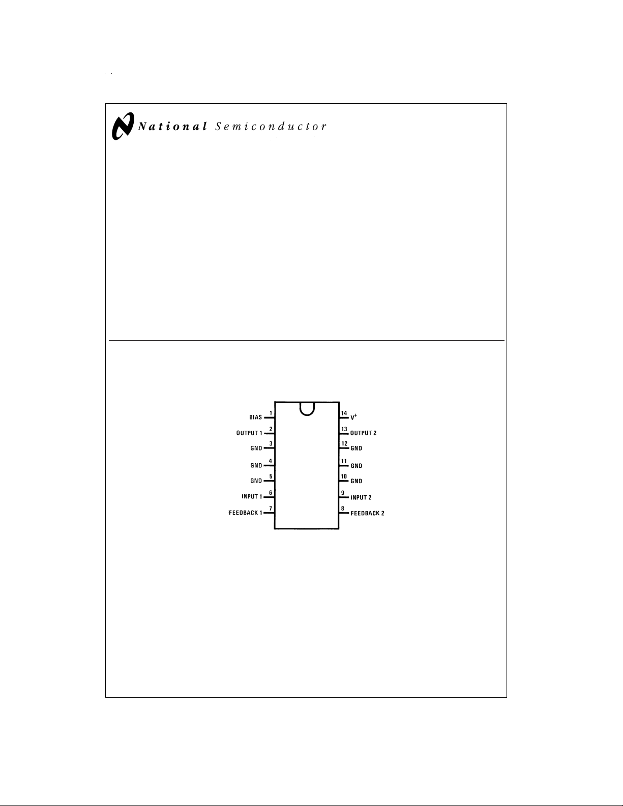
Connection Diagram
Dual-In-Line Package
or Surface Mount Package
DS007913-1
Top View
Order Number LM1877M-9 or LM1877N-9
See NS Package Number M14B or N14A
© 1999 National Semiconductor Corporation DS007913 www.national.com
Page 2
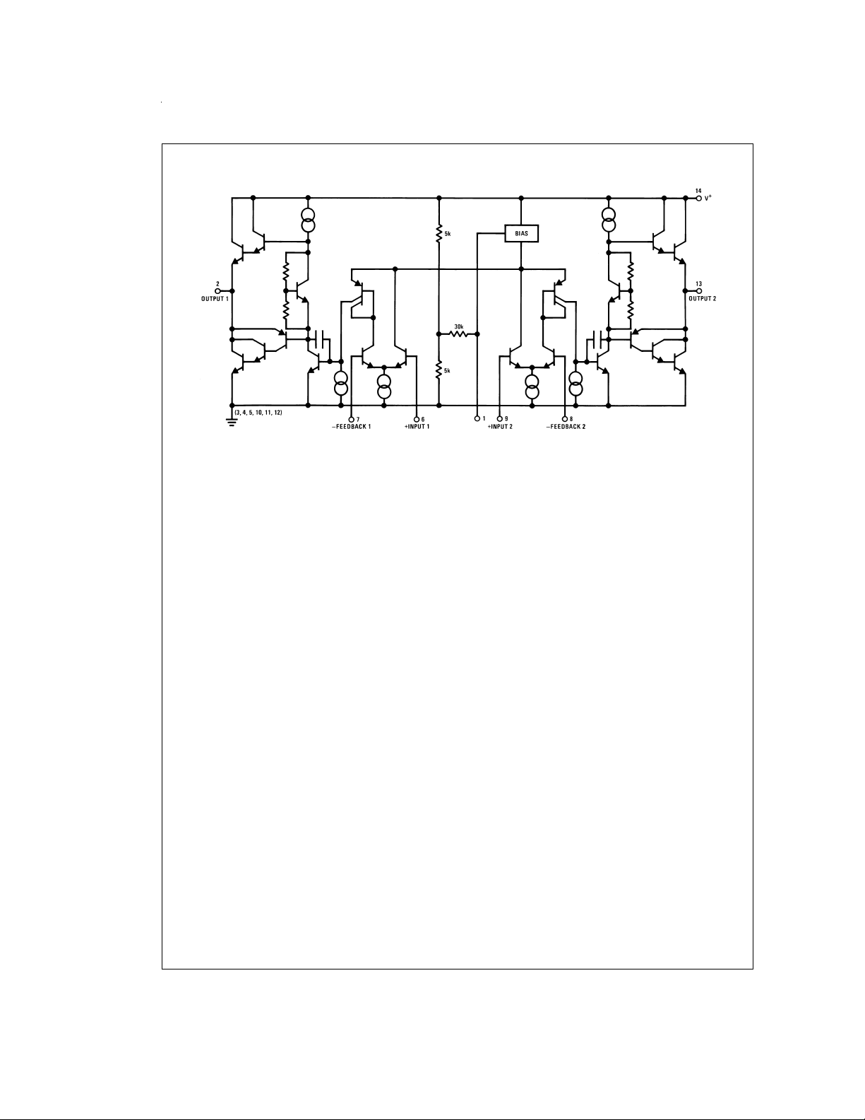
Equivalent Schematic Diagram
DS007913-2
www.national.com 2
Page 3
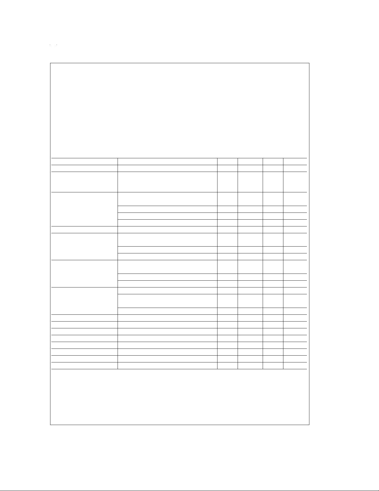
Absolute Maximum Ratings (Note 1)
If Military/Aerospace specified devices are required,
please contact the National Semiconductor Sales Office/
Distributors for availability and specifications.
Supply Voltage 26V
Input Voltage
Operating Temperature 0˚C to +70˚C
Storage Temperature −65˚C to +150˚C
Junction Temperature 150˚C
±
0.7V
M-Package Infared (15 sec.) 220˚C
M-Package Vapor Phase (60 sec.) 215˚C
Thermal Resistance
(N-Package) 30˚C/W
θ
JC
(N-Package) 79˚C/W
θ
JA
(M-Package) 27˚C/W
θ
JC
(M-Package) 114˚C/W
θ
JA
Note 1: Absolute Maximum Ratings indicate limits beyond which damage to
the device may occur.Operating Ratings indicate conditions for which thedevice is functional, but do not guarantee specific performance limits.
Lead Temperature
N-Package Soldering (10 sec.) 260˚C
Electrical Characteristics
=
V
S
Total Supply Current P
Output Power THD=10
LM1877 V
Total Harmonic Distortion
LM1877 f=1 kHz, V
Output Swing R
Channel Separation C
PSRR Power Supply C
Rejection Ratio f=120 Hz, Output Referred
Noise Equivalent Input Noise
Open Loop Gain R
Input Offset Voltage 15 mV
Input Bias Current 50 nA
Input Impedance Open Loop 4 MΩ
DC Output Level V
Slew Rate 2.0 V/µs
Power Bandwidth 65 kHz
Current Limit 1.0 A
Note 2: For operation at ambient temperature greater than 25˚C, the LM1877 must be derated based on a maximum 150˚C junction temperature.
20V, T
=
25˚C, (Note 2) R
A
L
=
8Ω,A
=
50 (34 dB) unless otherwise specified
V
Parameter Conditions Min Typ Max Units
=
0W 25 50 mA
O
%
=
S
=
V
S
=
P
O
=
P
O
=
P
O
=
L
=
F
=
20V, R
12V, R
8Ω 2.0 W/Ch
L
=
8Ω 1.3 W/Ch
L
=
14V
S
50 mW/Channel 0.075
500 mW/Channel 0.045
1 W/Channel 0.055
8Ω V
50 µF, C
=
0.1 µF,
IN
S
−6 Vp-p
f=1 kHz, Output Referred
=
V
S
=
V
S
=
F
=
V
S
=
V
S
=
R
S
=
20V, V
7V, V
50 µF, C
20V, V
7V, V
0, C
4 Vrms −50 −70 dB
O
=
0.5 Vrms −60 dB
O
=
0.1 µF,
IN
=
1 Vrms −50 −65 dB
RIPPLE
=
0.5 Vrms −40 dB
RIPPLE
=
0.1 µF, 2.5 µV
IN
BW=20 Hz–20 kHz, Output Noise Wideband
=
R
S
S
S
=
0, C
0.1 µF, A
N
=
0, f=100 kHz, R
=
20V 9 10 11 V
200 0.80 mV
V
=
8Ω 70 dB
L
%
%
%
www.national.com3
Page 4

Typical Performance Characteristics
Device Dissipation vs
Ambient Temperature
DS007913-10
Power Supply Rejection Ratio
(Referred to the Output) vs
Supply Voltage
DS007913-13
Power Supply Rejection Ratio
(Referred to the Output) vs
Frequency
DS007913-11
Channel Separation (Referred
to the Output) vs Frequency
DS007913-14
Power Supply Rejection Ratio
(Referred to the Output) vs
Frequency
DS007913-12
Channel Separation (Referred
to the Output) vs Frequency
DS007913-15
Average Supply Current vs
P
OUT
DS007913-16
www.national.com 4
Total Harmonic Distortion
vs Frequency
DS007913-17
Total Harmonic Distortion
vs Frequency
DS007913-18
Page 5

Typical Performance Characteristics (Continued)
Power Dissipation (W)
Both Channels Operating
DS007913-19
Typical Applications
Open Loop Gain vs
Frequency
DS007913-20
Output Swing vs Supply
Voltage
Stereo Phonograph Amplifier with Bass Tone Control
DS007913-21
DS007913-4
www.national.com5
Page 6

Typical Applications (Continued)
Frequency Response of Bass Tone Control
DS007913-5
Stereo Amplifier with A
Inverting Unity Gain Amplifier
=
200
V
DS007913-6
www.national.com 6
DS007913-7
Page 7

Typical Applications (Continued)
Non-Inverting Amplifier Using Split Supply
Typical Split Supply
DS007913-9
DS007913-8
www.national.com7
Page 8

Physical Dimensions inches (millimeters) unless otherwise noted
Molded SOIC Package (M)
Order Number LM1877M-9
NS Package Number M14B
www.national.com 8
Page 9

Physical Dimensions inches (millimeters) unless otherwise noted (Continued)
Molded Dual-In-Line Package (N)
Order Number LM1877N-9
NS Package Number N14A
LM1877 Dual Audio Power Amplifier
LIFE SUPPORT POLICY
NATIONAL’S PRODUCTS ARE NOT AUTHORIZED FOR USE AS CRITICAL COMPONENTS IN LIFE SUPPORT
DEVICES OR SYSTEMS WITHOUT THE EXPRESS WRITTEN APPROVAL OF THE PRESIDENT AND GENERAL
COUNSEL OF NATIONAL SEMICONDUCTOR CORPORATION. As used herein:
1. Life support devices or systems are devices or
systems which, (a) are intended for surgical implant
into the body, or (b) support or sustain life, and
whose failure to perform when properly used in
accordance with instructions for use provided in the
2. A critical component is any component of a life
support device or system whose failure to perform
can be reasonably expected to cause the failure of
the life support device or system, or to affect its
safety or effectiveness.
labeling, can be reasonably expected to result in a
significant injury to the user.
National Semiconductor
Corporation
Americas
Tel: 1-800-272-9959
Fax: 1-800-737-7018
Email: support@nsc.com
www.national.com
National does not assume any responsibility for use of any circuitry described, no circuit patent licenses are implied and National reserves the right at any time without notice to change said circuitry and specifications.
National Semiconductor
Europe
Fax: +49 (0) 1 80-530 85 86
Email: europe.support@nsc.com
Deutsch Tel: +49 (0) 1 80-530 85 85
English Tel: +49 (0) 1 80-532 78 32
Français Tel: +49 (0) 1 80-532 93 58
Italiano Tel: +49 (0) 1 80-534 16 80
National Semiconductor
Asia Pacific Customer
Response Group
Tel: 65-2544466
Fax: 65-2504466
Email: sea.support@nsc.com
National Semiconductor
Japan Ltd.
Tel: 81-3-5639-7560
Fax: 81-3-5639-7507
 Loading...