

Page 1
LM1868 AM/FM Radio System
LM1868 AM/FM Radio System
February 1995
General Description
The combination of the LM1868 and an FM tuner will provide all the necessary functions for a 0.5 watt AM/FM radio.
Included in the LM 1868 are the audio power amplifier, FM
IF and detector, and the AM converter, IF, and detector.
The device is suitable for both line operated and 9V battery
applications.
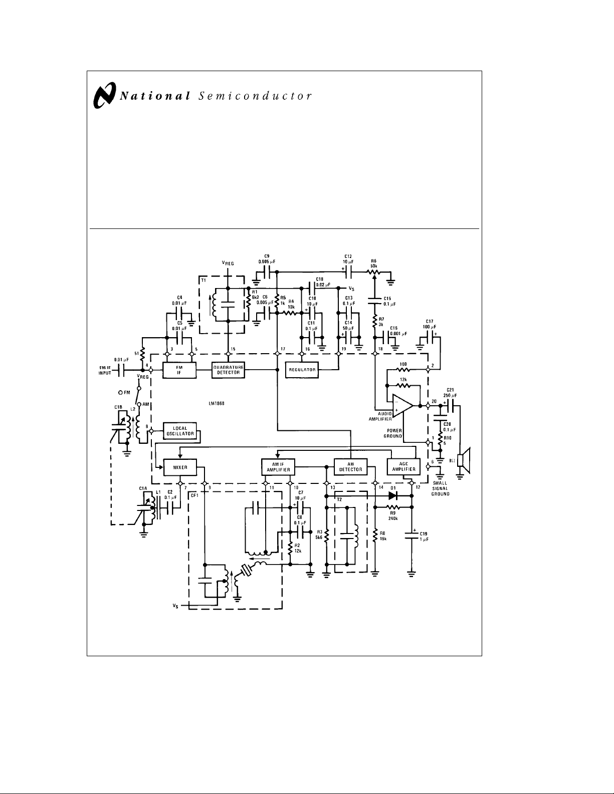
Block Diagram
Features
Y
DC selection of AM/FM mode
Y
Regulated supply
Y
Audio amplifier bandwidth decreased in AM mode,
reducing amplifier noise in the AM band
Y
AM converter AGC for excellent overload
characteristics
Y
Low current internal AM detector for low tweet radiation
Order Number LM1868N
TL/H/7909– 1
See NS Package Number N20A
Note: See table for coil data
C
1995 National Semiconductor Corporation RRD-B30M115/Printed in U. S. A.
TL/H/7909
Page 2
Absolute Maximum Ratings
If Military/Aerospace specified devices are required,
please contact the National Semiconductor Sales
Office/Distributors for availability and specifications.
Supply Voltage (Pin 19) 15V
Package Dissipation 2.0W
Above T
T
Electrical Characteristics Test Circuit, T
J(MAX)
e
25§C, Derate Based on
A
e
150§C and i
e
60§C/W
JA
A
Storage Temperature Range
Operating Temperature Range 0§Ctoa70§C
Lead Temperature (Soldering, 10 sec.) 260§C
e
25§C, V
e
S
9V, R
e
8X (unless otherwise noted)
L
Parameter Conditions Min Typ Max Units
STATIC CHARACTERISTICS e
AM
e
0, e
FM
e
0
Supply Current AM Mode, S1 in Position 1 22 30 mA
Regulator Output Voltage (Pin 16) 3.5 3.9 4.8 V
Operating Voltage Range 4.5 15
DYNAMIC CHARACTERISTICSÐAM MODE
e
1 MHz, f
f
AM
Maximum Sensitivity Measure eAMfor P
Signal-to-Noise e
Detector Output e
Overload Distortion e
Total Harmonic Distortion (THD) e
DYNAMIC CHARACTERISTICSÐFM MODE f
b
3 dB Limiting Sensitivity 15 45 mV
Signal-to-Noise Ratio e
Detector Output e
AM Rejection e
Total Harmonic Distortion (THD) e
DYNAMIC CHARACTERISTICSÐAUDIO AMPLIFIER ONLY fe1 kHz, e
e
1 kHz, 30% Modulation, S1 in Position 1, P
mod
Maximum Volume
AM
AM
Measure at Top of Volume Control
AM
AM
FM
FM
FM
Measure at Top of Volume Control
FM
FM
e
50 mW unless noted
O
e
50 mW,
O
e
10 mV 40 50 dB
e
1mV
e
50 mV, 80% Modulation 2 10 %
e
10 mV 1.1 2 %
e
10.7 MHz, f
e
10 mV 50 64 dB
e
10 mV, Df
e
10 mV, 30% AM Modulation 40 50 dB
e
10 mV 1.1 2 %
mod
e
e
g
22.5 kHz
400 Hz, Df
e
AM
816mV
40 60 85 mV
e
g
75 kHz, P
e
50 mW, S1 in Position 1
O
40 60 85 mV
e
0, e
0, S1 in Position 2
FM
Power Output THDe10%, RL8X
e
6V 250 325 mW
V
S
e
9V 500 700 mW
V
S
Bandwidth AM Mode, P
FM Mode, P
Total Harmonic Distortion (THD) P
e
O
e
50 mW 11 kHz
O
e
50 mW 22 kHz
O
50 mW, FM Mode 0.2 %
Voltage Gain 41 dB
b
55§Ctoa150§C
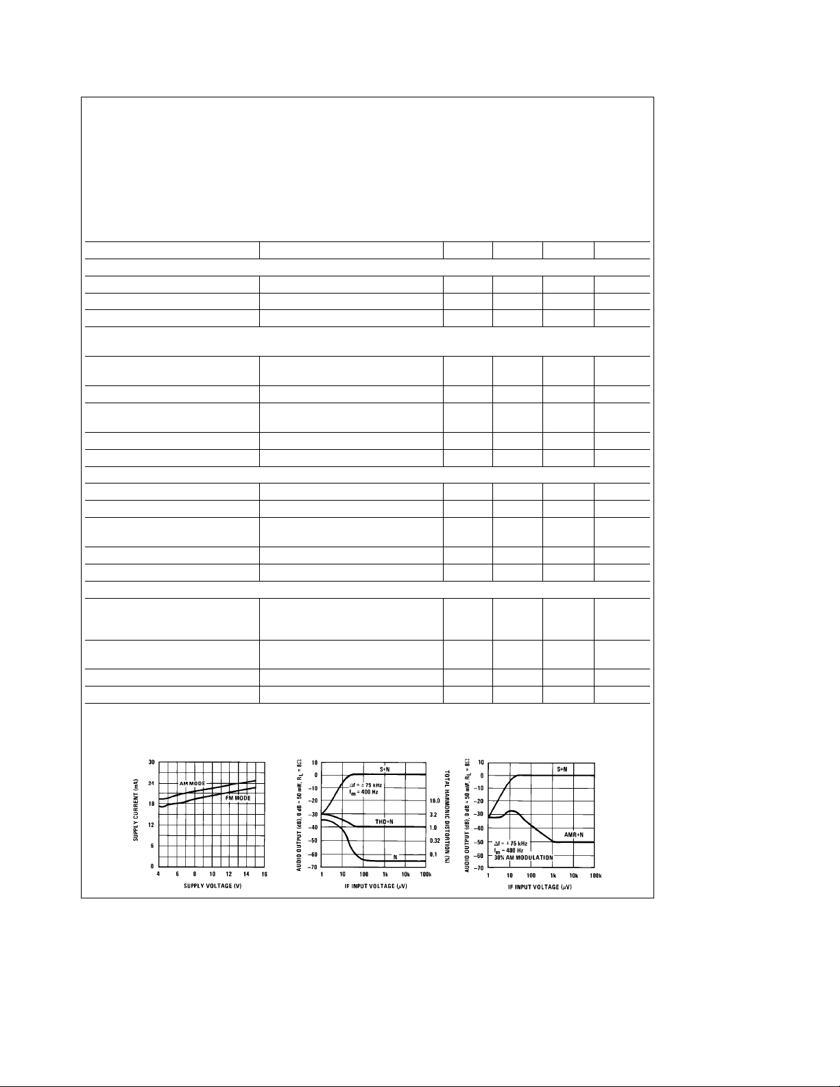
Typical Performance Characteristics (Test Circuit) All curves are measured at audio output
Quiescent Supply Current
vs Voltage
FM Limiting Characteristics FM IF AM Rejection
2
TL/H/7909– 2
Page 3
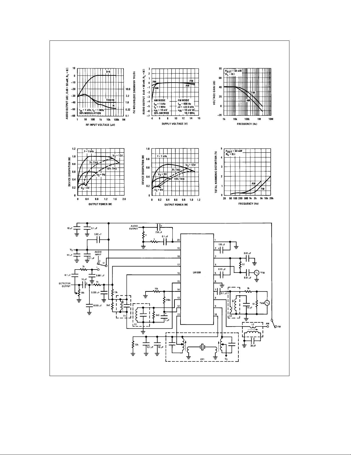
Typical Performance Characteristics (Continued)
All curves are measured at audio output (Test Circuit)
AM Characteristics
Recovered Audio vs Supply Amplifier Only
Gain vs Frequency Audio
Power Dissipation vs Power
Output, R
Test Circuit
e
8X
L
Power Dissipation vs Power
e
Out, R
16X
L
Distortion vs Frequency
Audio Amplifier Only
TL/H/7909– 3
Note: See table for coil data TL/H/7909– 4
3
Page 4

Typical Application
TL/H/7909– 5
Maximum sensitivity: 100 mV/m
20 dB quieting sensitivity: 250 mV/m#Tweet* worst case: 5%
100 mV/m: 1.5%
#
#
FM Performance (88 MHz –108 MHz) AM Performance (525 kHz –1650 kHz)
3 dB limiting sensitivity: 7 mV
b
30 dB quieting sensitivity: 3.5 mV
#
#
*Tweet is an audio tone produced by the 2nd and 3rd harmonic of the IF
beating against the received signal. It is measured as an equivalent modu-
lation level: i.e., a 30% tweet has the same amplitude at the detector as a
desired signal with 30% modulation.
4
Page 5

PC Board Layout
Component Side
Typical Performance Characteristics Typical Application
All curves are measured at audio output
TL/H/7909– 7 TL/H/7909– 8
TL/H/7909– 6
5
Page 6

IC External Components (Application Circuit)
Component
C1 100 pF Removes tuner LO from IF input
C2 0.1 mF Antenna coupling capacitor
C4, C5 0.01 mF FM IF decoupling capacitors
C6, C9 0.005 mF AM smoothing/FM de-emphasis
R5 1k
C10 10 mF Regulator decoupling capacitor
C11 0.1 mF Regulator decoupling capacitor
C12 10mF AC coupling to volume control
C13 0.1 mF Power supply decoupling
C14 50 mF Power supply decoupling
C15 0.1 mF Audio amplifier input coupling
R7 3k Roll off signals from detector in
C16 0.001 mF
C17 100 mF Power amplifier feedback
R8 16k AM detector bias resistor
Typical
Value
Comments
network, de-emphasis pole is
(
given by.
j
f1
2q (C6aC9)
the AM band to prevent radiation
(
1
#
R4 R6
R4aR6
decoupling, sets low frequency
supply rejection
J
Coil and Tuning Capacitor Specifications
C1 AM ANT 140 pF max 5.0 pF min FM 20 pF max 4.5 pF min
AM OSC 82 pF max 5.0 pF min TOKO CY2-22124PT
Trimmers 5 pF
L1 640 mH, Q
L0, L2 360 mH, Q
e
200 AM antenna
u
e
3k5@Fe796 kHz 1 mV/meter induces
R
P
(At secondary) approximately 100 mV
l
e
80@F
U
open circuit at the secondary
796 kHz TOKO RWO-6A5105 or
equivalent
Toko America
1250 Feehanville Drive
Mount Prospect, IL 60056
(312) 297-0070
Component
Typical
Value
Comments
R9 240k Set AGC time constant
C19 1 mF
(
C7 10 mF IF coupling
C8 0.1 mF IF coupling
C20 0.1 mF High frequency load for audio
amplifier, required to stabilize
R10 5X
(
audio amplifier
C21 250 mF Output coupling capacitor
R1 6k2 Sets Q of quadrature coil,
determining FM THD and
recovered audio
R2 12k IF amplifier bias R
R3 5k6 Sets gain of AM IF and Q of AM
IF output tank
R4 10k Detector load resistor
R6 50k Volume control
C18 0.02 mF Power supply decoupling
R11, R12 150X Terminates the ceramic filter,
biases FM IF input stage
D1 1N4148 Optional. Quickens the AGC
response during turn on
l
T1 Q
TL/H/7909– 10
T2 Q
70@10.7 MHz, L to
u
resonate w/82 pF
TOKO KAC-K2318 or equivalent
l
14@455 kHz, L to
u
resonate w/180 pF
TOKO 159GC-A3785 or
equivalent
@
10.7 MHz
@
455 kHz
L4 SWGÝ20, Ne3(/2T, inner
diameter
L5 SWG
diameter
L6 L
L7 SWG
diameter
CF2 10.7 MHz ceramic filter Murata
MURATA SFE 10.7 mA or 2200 Lake Park Drive
equivalent Smyrna, GA 30080
TL/H/7909– 9
e
5mm
Ý
20, Ne3(/2T, inner
e
5mm
e
0.44 mH, Ne4 (/2T, Que70
Ý
20, Ne2 (/2T, inner
e
5mm
(404) 436-1300
TL/H/7909– 11
CF1 TOKO CFU-090D or equivalent
TL/H/7909– 12
T3 Apollo Electronics NS-107C
TL/H/7909– 13
l
4.8 kHz@455 kHz
BW
or equivalent
6
Page 7

Layout Considerations
AM SECTION
Most problems in an AM radio design are associated with
radiation of undesired signals to the loopstick. Depending
on the source, this radiation can cause a variety of problems
including tweet, poor signal-to-noise, and low frequency oscillation (motor boating). Although the level of radiation from
the LM1868 is low, the overall radio performance can be
degraded by improper PCB layout. Listed below are layout
considerations association with common problems.
1. Tweet: Locate the loopstick as far as possible from detector components C6, C9, R4, and R5. Orient C6, C9, R4,
and R5 parallel to the axis of the loopstick. Return R8, C6,
C9, and C19 to a separate ground run (see Typical Application PCB).
2. Poor Signal-to-Noise/Low Frequency Oscillation:
Twist speaker leads. Orient R10 and C20 parallel to the axis
of the loopstick. Locate C11 away from the loopstick.
TL/H/7909– 14
In general, radiation results from current flowing in a loop. In
case 1 this current loop results from decoupling detector
harmonics at pin 17; while in case 2, the current loop results
from decoupling noise at the output of the audio amplifier
and the output of the regulator. The level of radiation picked
up by the loopstick is approximately proportional to: 1) 1/r
where r is the distance from the center of the loopstick to
the center of the current loop; 2) SIN i, where i is the angle
between the plane of the current loop and the axis of the
loopstick; 3) I, the current flowing in the loop; and 4) A, the
cross-sectional area of the current loop.
Pickup is kept low by short leads (low A), proper orientation
(ij0soSINij0), maximizing distance from sources to
loopstick, and keeping current levels low.
FM SECTION
The pinout of the LM1868 has been chosen to minimize
layout problems, however some care in layout is required to
insure stability. The input source ground should return to C4
ground. Capacitors C13 and C18 form the return path for
signal currents flowing in the quadrature coil. They should
connect directly to the proper pins with short PC traces (see
Typical Application PCB). The quadrature coil and input circuitry should be separated from each other as far as possible.
AUDIO AMPLIFIER
The standard layout considerations for audio amplifiers apply to the LM1868, that is: positive and negative inputs
should be returned to the same ground point, and leads to
the high frequency load should be kept short. In the case of
the LM1868 this means returning the volume control ground
(R6) to the same ground point as C17, and keeping the
leads to C20 and R10 short.
Circuit Description (See Equivalent Schematic)
AM SECTION
The AM section consists of a mixer stage, a separate local
oscillator, an IF gain block, an envelope detector, AGC circuits for controlling the IF and mixer gains, and a switching
circuit which disables the AM section in the FM mode.
Signals from the antenna are AC-coupled into pin 7, the
mixer input. This stage consists of a common-emitter amplifier driving a differential amp which is switched by the local
oscillator. With no mixer AGC, the current in the mixer is
330 mA; as the AGC is applied, the mixer current drops,
decreasing the gain, and also the input impedance drops,
reducing the signal at the input. The differential amp connected to pin 8 forms the local oscillator. Bias resistors are
arranged to present a negative impedance at pin 8. The
frequency of oscillation is determined by the tank circuit, the
peak-to-peak amplitude is approximately 300 mA times the
impedance at pin 8 in parallel with 8k2.
After passing through the ceramic filter, the IF signals are
applied to the IF input. Signals at pin 11 are amplified by two
AGC controlled common-emitter stages and then applied to
the PNP output stage connected to pin 13. Biasing is arranged so that the current in the first two stages is set by
the difference between a 250 mA current source and the
Darlington device connected to pin 12.
When the AGC threshold is exceeded, the Darlington device
turns ON, steering current away from the IF into ground,
reducing the IF gain. Current in the IF is monitored by the
mixer AGC circuit. When the current in the IF has dropped
to 30 mA, corresponding to 30 dB gain reduction in the IF,
the mixer AGC line begins to draw current. This causes the
mixer current and input impedance to drop, as previously
described.
The IF output is level shifted and then peak detected at
detector cap C1. By loading C1 with only the base current of
the following device, detector currents are kept low. Drive
from the AGC is taken at pin 14, while the AM detector
3
;
output is summed with the FM detector output at pin 17.
FM SECTION
The FM section is composed of a 6-stage limiting IF driving
a quadrature detector. The IF stages are identical with the
exceptions of the input stage, which is run at higher current
to reduce noise, and the last stage, which is switched OFF
in the AM mode. The quadrature detector collectors drive a
level shift arrangement which allows the detector output
load to be connected to the regulated supply.
AUDIO AMPLIFIER
The audio amplifier has an internally set voltage gain of 120.
The bandwidth of the audio amplifier is reduced in the AM
mode so as to reduce the output noise falling in the AM
band. The bandwidth reduction is accomplished by reducing
the current in the input stage.
REGULATOR
A series pass regulator provides biasing for the AM and FM
sections. Use of a PNP pass device allows the supply to
drop to within a few hundred millivolts of the regulator output and still be in regulation.
7
Page 8

Equivalent Schematic
TL/H/7909– 15
8
Page 9

9
Page 10

Physical Dimensions inches (millimeters)
LM1868 AM/FM Radio System
Molded Dual-In-Line Package (N)
Order Number LM1868N
NS Package Number N20A
LIFE SUPPORT POLICY
NATIONAL’S PRODUCTS ARE NOT AUTHORIZED FOR USE AS CRITICAL COMPONENTS IN LIFE SUPPORT
DEVICES OR SYSTEMS WITHOUT THE EXPRESS WRITTEN APPROVAL OF THE PRESIDENT OF NATIONAL
SEMICONDUCTOR CORPORATION. As used herein:
1. Life support devices or systems are devices or 2. A critical component is any component of a life
systems which, (a) are intended for surgical implant support device or system whose failure to perform can
into the body, or (b) support or sustain life, and whose be reasonably expected to cause the failure of the life
failure to perform, when properly used in accordance support device or system, or to affect its safety or
with instructions for use provided in the labeling, can effectiveness.
be reasonably expected to result in a significant injury
to the user.
National Semiconductor National Semiconductor National Semiconductor National Semiconductor
Corporation Europe Hong Kong Ltd. Japan Ltd.
1111 West Bardin Road Fax: (
Arlington, TX 76017 Email: cnjwge@tevm2.nsc.com Ocean Centre, 5 Canton Rd. Fax: 81-043-299-2408
Tel: 1(800) 272-9959 Deutsch Tel: (
Fax: 1(800) 737-7018 English Tel: (
National does not assume any responsibility for use of any circuitry described, no circuit patent licenses are implied and National reserves the right at any time without notice to change said circuitry and specifications.
Fran3ais Tel: (
Italiano Tel: (
a
49) 0-180-530 85 86 13th Floor, Straight Block, Tel: 81-043-299-2309
a
49) 0-180-530 85 85 Tsimshatsui, Kowloon
a
49) 0-180-532 78 32 Hong Kong
a
49) 0-180-532 93 58 Tel: (852) 2737-1600
a
49) 0-180-534 16 80 Fax: (852) 2736-9960
 Loading...