

Page 1
TL/H/7509
LM1865 Advanced FM IF System
February 1995
LM1865 Advanced FM IF System
General Description
Reduced external component cost, improved performance,
and additonal functions are key features to the LM1865 FM
IF system. The LM1865 is designed for use in electronically
tuned radio applications. It contains both deviation and signal level stop circuitry in addition to an open-collector stop
output. The LM1865 generates a reverse AGC voltage (ie:
decreasing AGC voltage with increasing signal).
Features
Y
On-chip buffer to provide gain and terminate two ceramic filters
Y
Low distortion 0.1% typical with a single tuned quadrature coil for 100% modulation.
Y
Broad off frequency distortion characteristic
Y
Low THD at minimum AFT offset
Y
Meter output proportional to signal level
Y
Stop detector with open-collector output
Y
Adjustable signal level mute/stop threshold, controlled
either by ultrasonic noise in the recovered audio or by
the meter output
Y
Adjustable deviation mute/stop threshold
Y
Separate time constants for signal level and deviation
mute/stop
Y
Dual threshold AGC eliminates need for local/distance
switch and offers improved immunity from third order intermodulation products due to tuner overload
Y
User control of both AGC thresholds
Y
Excellent signal to noise ratio, AM rejection and system
limiting sensitivity
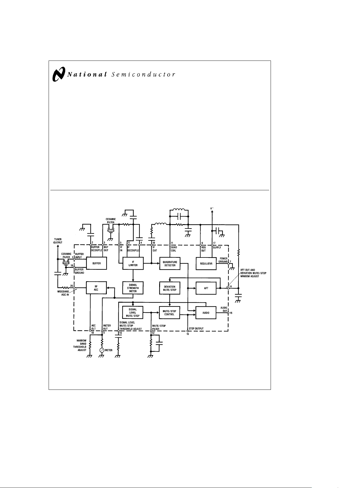
Block Diagram
Order Number LM1865M
or LM1865N
See NS Package Number
M20B or N20A
TL/H/7509– 1
FIGURE 1
C
1995 National Semiconductor Corporation RRD-B30M115/Printed in U. S. A.
Page 2
Absolute Maximum Ratings
If Military/Aerospace specified devices are required,
please contact the National Semiconductor Sales
Office/Distributors for availability and specifications.
Supply Voltage, Pin 17 16V
Package Dissipation (Note 1) 2.0W
Storage Temperature Range
b
55§Ctoa150§C
Operating Temperature Range
b
20§Ctoa85§C
Max Voltage on Pin 16 (Stop Output) 16V
Soldering Information
Dual-In-Line Package
Soldering (10 seconds) 260
§
C
Small Outline Package
Vapor Phase (60 seconds) 215
§
C
Infrared (15 seconds) 220
§
C
See AN-450 ‘‘Surface Mounting Methods and Their Effect
on Product Reliability’’ for other methods of soldering surface mount devices.
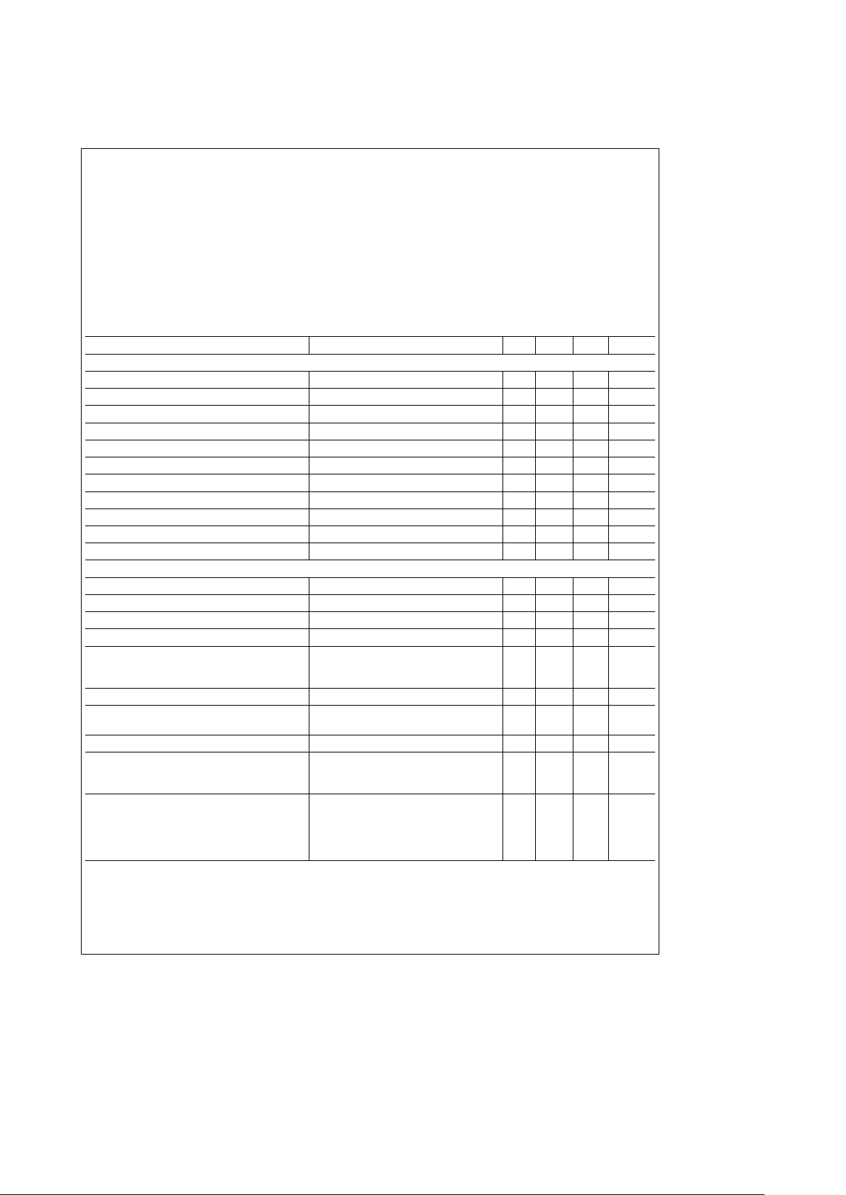
Electrical Characteristics
Test Circuit, T
A
e
25§C, V
a
e
12V; S1 in position 2; S2 in position 1; and S3 in position 2 unless indicated otherwise
Parameter Conditions Min Typ Max Units
STATIC CHARACTERISTICS
Supply Current 33 45 mA
Pin 9, Regulator Voltage 5.7 V
Operating Voltage Range (See Note 2) 7.3 16 V
Pin 18, Output Leakage Current Pin 20 Open, V
IF
e
0, S3 in Position 1 0.1 mA
Pin 16, Stop Low Output Voltage S1 in Position 1, S2 in Position 3 0.3 V
Pin 16, Stop High Output Leakage Current S2 in Position 2, V14eV9 0.1 mA
Pin 15, Audio Output Resistance 4.7 kX
Pin 1, Buffer Input Resistance Measured at DC 350 X
Pin 3, Buffer Output Resistance Measured at DC 350 X
Pin 20, Wide Band Input Resistance Measured at DC 2 X
Pin 8, Meter Output Resistance 1kX
DYNAMIC CHARACTERISTICS f
MOD
e
400 Hz, f
o
e
10.7 MHz, Deviation
e
g
75 kHz
b
3 dB Limiting Sensitivity IF Only (See Note 3) 60 120 mVrms
Buffer Voltage Gain VINPin 1e10 mVrms at 10.7 MHz 19 22 25 dB
Recovered Audio V
IF
e
10 mVrms, V14eV9 275 320 470 mVrms
Signal-to-Noise V
IF
e
10 mVrms, V14eV9 (See Note 4) 70 84 dB
AM Rejection V14eV9
V
IF
e
1 mV, 30% AM Mod 50 60 dB
V
IF
e
10 mV, 30% AM Mod 50 60 dB
Minimum Total Harmonic Distortion V
IF
e
10 mV 0.1 0.35 %
THD at Frequency where V14eV9 V
IF
e
10 mV, Tune until V14eV9 0.1 0.45 %
(Zero AFT Offset)
THDg10 kHz from Frequency where V14eV9 V
IF
e
10 mV 0.15 %
AFT Offset Frequency for Low V
IF
e
10 mV, S2 in Position 3, f
MOD
e
0
g
50 kHz
Stop Output at Pin 16 Offsete(Frequency for Pin 16 Low)
b
(Frequency where V14eV9)
Ultrasonic Mute/Stop Level Threshold V14eV9, S1 in Position 3 (See Note 5) 60 kHz
V
IF
e
10 mV
f
MOD
e
100 kHz
S2 in Position 3
Amount of Deviation where V16
x
Low
2
Page 3
Electrical Characteristics Test Circuit, T
A
e
25§C, V
a
e
12V; S1 in position 2; S2 in position 1; and S3 in
position 2 unless indicated otherwise (Continued)
Parameter Conditions Min Typ Max Units
DYNAMIC CHARACTERISTICS f
MOD
e
400 Hz, f
o
e
10.7 MHz, Deviation
e
g
75 kHz (Continued)
Pin 13 Mute/Stop Threshold Voltage V14eV9, S1 in Position 4 220 mV
S2 in Position 3
V13 where V16
x
Low
Amount of Muting (LM1965 Only) S2 in Position 4, S1 in Position 1, V
IF
e
10 mV 66 dB
Amount of Muting with Pin 13 and S1 in Position 1 0 dB
Pin 16 Grounded V14,
e
V9, V
IF
e
10 mV
Narrow Band AGC Threshold Increase IF Input until I
AGC
e
0.1 mA 100 210 300 mVrms
Pin 20
e
30 mVrms
Wide Band AGC Threshold V
IF
e
100 mVrms 5 12 22 mVrms
Increase Signal to Pin 20 until I
AGC
e
0.1 mA
Pin 18, Low Output Voltage VINPin 20e100 mV, V
IF
e
100 mVrms 0.2 0.5 V
(LM1865 and LM1965 only)
Pin 18, High Output Voltage (LM2065 only) VINPin 20e100 mV, V
IF
e
100 mVrms, (See Note 6) 11.7 V
Pin 8, Meter Output Voltage V
IF
e
10 mV 0.1 V
V
IF
e
300 mV 1.1 V
V
IF
e
3 mV 2.6 V
Note 1: Above T
A
e
25§C derate based on T
J(max)
e
150§C and i
JA
e
60§C/W.
Note 2: All data sheet specifications are for V
a
e
12V may change slightly with supply.
Note 3: When the IF is preceded by 22 dB gain in the buffer, excellent system sensitivity is achieved.
Note 4: Measured with a notch at 60 Hz and 20 Hz to 100 kHz bandwidth.
Note 5: FM modulate RF source with a 100 kHz audio signal and find what modulation level, expressed as kHz deviation, results in V16
x
12V.
Test Circuit
TL/H/7509– 2
FIGURE 2
3
Page 4
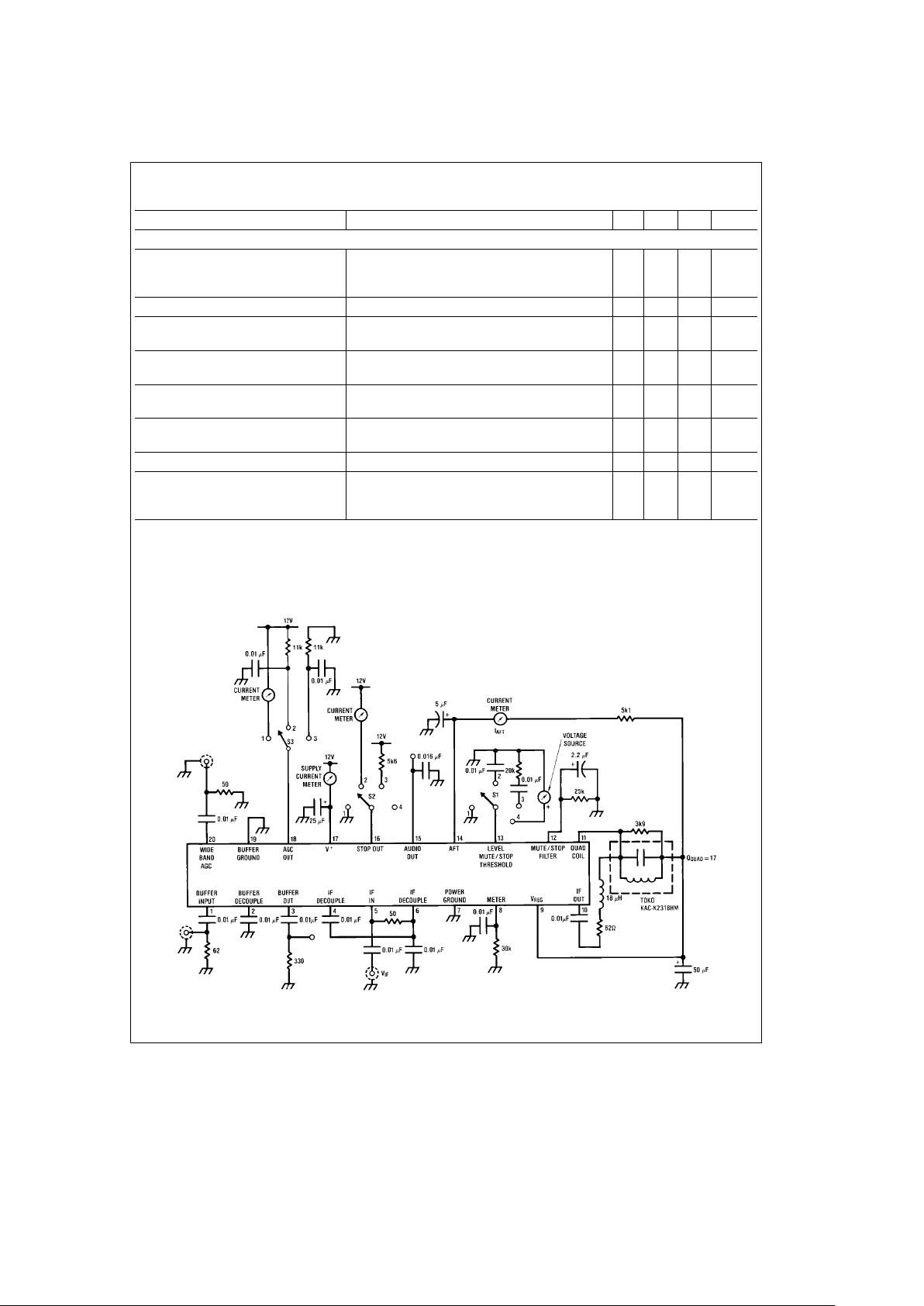
Typical Performance Characteristics (from Test Circuit)
FM Limiting Characteristics
and AM Rejection
Pin 8, Meter Output Voltage
vs IF Input Level
FM Limiting Characteristics
a
THD
% THD vs OFF Tuning
(Single Tuned Quadrature
Coil)
Deviation Mute/Stop
Threshold as a Function of
AFT Load Resistor
Supply Current vs
Supply Voltage
Pin 14, AFT Current
vs Tuning
TL/H/7509– 3
Coils and ceramic filters are available from:
Toko America
1250 Feehanville Drive
Mount Prospect, IL 60056
(312) 297-0070
Murata
2200 Lake Park Drive
Smyrna, GA 30080
(404) 436-1300
4
Page 5
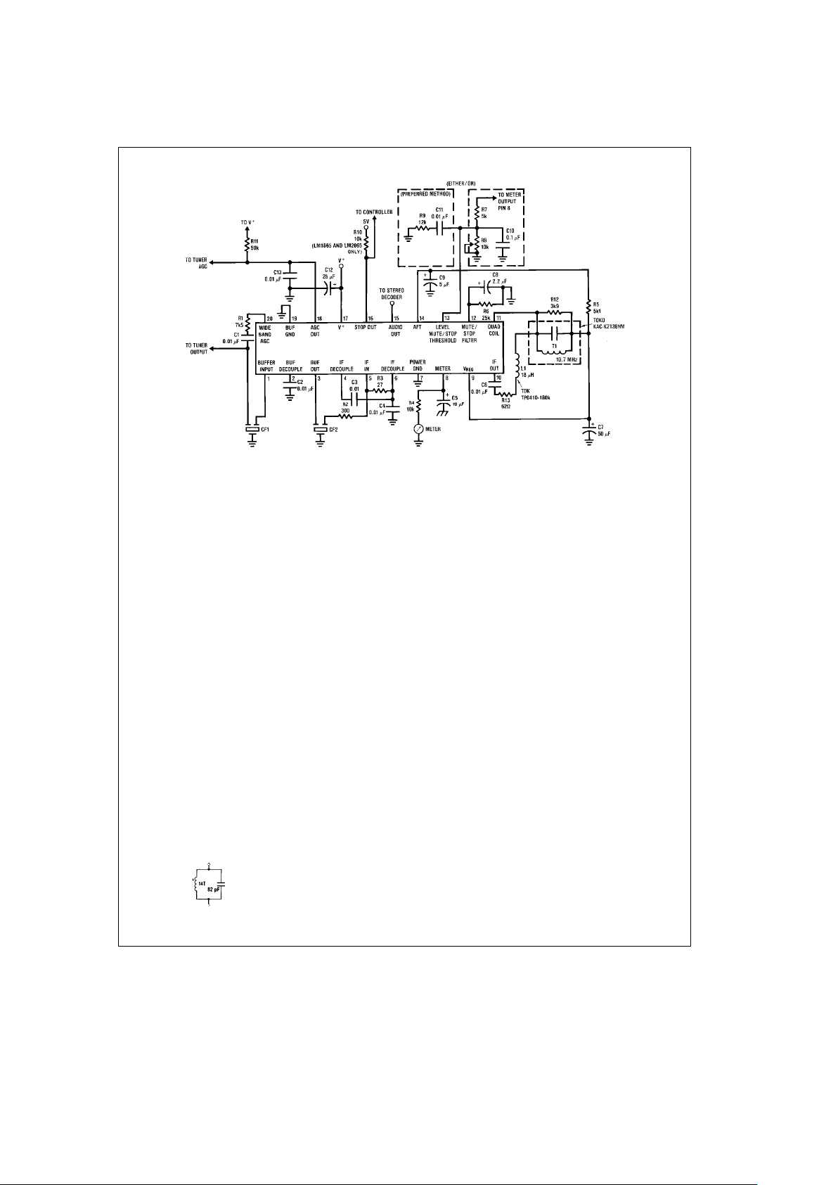
Application Circuit
TL/H/7509– 4
FIGURE 3
IC External Components (See Application Circuit)
Component Typical Value Comments
C1 0.01 mF AC coupling for wide band AGC input
C2 0.01 mF Buffer and AGC supply decoupling
C3, C4 0.01 mF IF decoupling capacitors
C5 10 mF Meter decoupling capacitor
C6 0.01 mF AC coupling for IF output
C7 50 mF Regulator decoupling capacitor, affects S/N floor
C8 2.2 mF Level mute/stop time constant
C9 5 mF AFT decoupling, affects stop time
C10 0.1 mF Disables noise mute/stop
C11 0.01 mF AC coupling for noise mute/stop threshold adjust
C12 25 mF Supply decoupling
C13 0.01 mF AGC output decoupling capacitor
R1 Tuner Dependent Wide band AGC threshold adjust
R2, R3 Tuner Dependent Gain set and bias for IF; R2
aR3e
330X to terminate ceramic filter
R4 Meter Dependent Sets full-scale on meter
R5 5k1 Deviation mute/stop window adjustment
R6 25k Mute/stop filter, affects stop time
R7 5k Level mute/stop threshold adjustment
R8 10k Pot Level mute/stop threshold adjustment
R9 12k Noise mute/stop threshold adjustment, decrease resistor for lower
S/N at threshold, for optimum performance over temp. and gain variation, set this resistor value so that the signal level mute/stop threshold
occurs in the radio at 45dB S/N (
g
3 dB) in mono.
R10 10k Load for open-collector stop output
R11 50k AGC output load resistor for open-collector output
R12 3k9 Sets Q of quadrature coil affecting THD, S/N and recovered audio
R13 62X Optimises minimum THD
L1 18 mHQ
u
l
50@10.7 MHz Sets signal swing across quadrature coil, High Q is important to miniTDK Electronics mize effect variation of Q has on both minimum THD and AFT offset.
TPO410-180K or equivalent
T1 Q
u
l
70@10.7 MHz, L to 10.7 MHz quadrature coil: Q
UL
l
70
resonate w/82 pF
@
10.7 MHz
TOKO KAC-K2318HM or
equivalent
CF1, CF2 10.7 MHz ceramic resonators provide selectivity; good group delay
Murata SFE10.7ML or equivalent
characteristics important for low THD of system
TL/H/7509– 5
5
Page 6

Typical Application
LAYOUT CONSIDERATIONS
Although the pinout of the LM1865 has been chosen to minimize layout problems, some care is required to insure stability. The ground terminal on CF1 should return to both
the input signal ground and the buffer ground, pin 19. The
ground terminal on CF2 should return to the ground side of
C4. The quadrature coil T1 and inductor L1 should be separated from the input circuitry as far as possible.
PC Layout (Component Side)
TL/H/7509– 6
PERFORMANCE CHARACTERISTICS OF TYPICAL
APPLICATION WITH TUNER
The following data was taken using the typical application
circuit in conjunction with an FM tuner with 43 dB of gain, a
5.5 dB noise figure, and 30 dB of AGC range. The tuner was
driven from a 50X source. 75 ms of de-emphasis was used
on the audio output, pin 15. The 0 dB reference is for
g
75
kHz deviation at 400 Hz modulation.
Meter Output and
Signal-to-Noise
vs Tuner Input
Total Harmonic Distortion vs
Tuner Input
AM Rejection vs Tuner
Input
TL/H/7509– 7
b
3 dB limitinge0.9 mV
30 dB quieting
e
1.4 mV
Level stop/mute threshold
e
1.4 mV
Deviation mute window (
b
3 dB)
e
g
45 kHz
6
Page 7

Application Notes
ADJUSTABLE MUTE/STOP THRESHOLD
The threshold adjustments for the mute and stop functions
are controlled by the same pins. Thus, the term mute/stop
will be used to designate either function.
The adjustable mute/stop threshold in the LM1865 allows
for user programming of the signal level at which muting or
stop indication takes place. The adjustment can be made in
two mutually exclusive ways. The first way is to take a voltage divider from the meter output (pin 8) to the off channel
mute input (pin 13). When the voltage at pin 13 falls below
0.22V, an internal comparator is tripped causing muted or
causing the stop output to go low. Adjustment of the voltage
divider ratio changes the signal level at which this happens.
The second method of mute/stop detection as a function of
signal level is to use the presence of ultrasonic noise in the
recovered audio to trip the internal comparator. As the signal level at the antenna of the radio drops, the amount of
noise in the recovered audio, both audible and ultrasonic,
increases.
The recovered audio is internally coupled through a high
pass filter to pin 13 which is internally biased above the
comparator trip point. Large negative-going noise spikes will
drive pin 13 below the comparator trip point and cause
mute/stop action. A simplified circuit is shown in
Figure 4
.
Since the input to the comparator is noise, the output of the
comparator is noise. Consequently, a mute/stop filter on pin
12 is required to convert output noise spikes to an average
DC value. This filter is not necessary if pin 13 is driven from
the meter.
Adjustment of the mute/stop threshold in the noise mode is
accomplished by adjusting the pole of the high pass filter
coupled to the comparator input. This is done with a series
capacitor/resistor combination, R9 C11, from pin 13 to
ground. As the pole is moved higher in frequency (i.e., R9
gets smaller) more ultrasonic noise is required in the recovered audio in order to initiate mute/stop action. This corre-
sponds to a weaker signal at the antenna of the radio. In
choosing the correct value for R9 it is important to make
sure that recovered audio below 75 kHz is not sufficient to
cause mute/stop action. This is because stereo and SCA
information are contained in the audio signal up to 75 kHz.
Also note that the ultrasonic mute/stop circuit will not operate properly unless a tuner is connected to the IF. This is
because, at low signal levels, the noise at the tuner output
dominates any noise sources in the IC. Consequently, driving the IC directly with a 50X generator is much less noisy
than driving the IC with a tuner and therefore not realistic.
The RC filter on pin 12 not only filters out noise from the
comparator output but controls the ‘‘feel’’ when manually
tuning. For example, a very long time constant will cause
the mute to remain active if you rapidly tune through valid
strong stations and will only release the mute if you slowly
tune to a valid station. Conversely, a short time constant will
allow the mute to kick in and out as one tunes rapidly
through valid stations.
The advantage in using the noise mute/stop approach versus the meter driven approach is that the point at which
mute/stop action occurs is directly related to the signal-tonoise ratio in the recovered audio. Furthermore, the mute/
stop threshold is not subject to production and temperature
variations in the meter output voltage at low signal levels,
and thus might be able to be set without a production adjustment of the radio. The noise mute/stop threshold is very
insensitive to temperature and gain variations. Proper operation of this circuit requires that the signal level mute/stop
threshold be set at a signal level that achieves 45 dB S/N
(
g
3 dB) in mono. in a radio. In an electronically tuned radio,
the signal level stop threshold can be set to a much larger
level by gain reducing the tuner (ie. pulling the AGC line) in
scan mode and then releasing the AGC once the radio
stops on a station. In an environment where temperature
variations are minimal and manual adjustment of the signal
level mute/stop threshold is desired, then the meter driven
approach is the best alternative.
TL/H/7509– 8
FIGURE 4. Simplified Level Mute/Stop Circuit
7
Page 8

Application Notes (Continued)
STOP TIME
An electronically tuned radio (ETR) pauses at fixed intervals
across the FM band and awaits the stop indication from the
LM1865. If within a predetermined period of time, no stop
indication is forthcoming, the controller circuit concludes
that there is no valid station at that frequency and will tune
to the next interval. There are several time constants that
can affect the amount of time it takes the LM1865 to output
a valid stop indication on pin 16. In this section each time
constant will be discussed.
Deviation Stop Time Constant
An offset voltage is generated by the AFT if the LM1865 is
tuned to either side of a station. Since deviation stop detection in the LM1865 is detected by the voltage at pin 14, it is
important that this voltage move fast enough to make the
deviation stop decision within the time allowed by the controller. The speed at which the voltage at pin 14 moves is
governed by the RC time constant, R5 C9. This time constant must be chosen long enough to remove recovered
audio from pin 14 and short enough to allow for reasonable
stop detection time.
Signal Level Stop Using Ultrasonic Noise Detection
As previously mentioned, the R6 C8 time constant on pin 12
is necessary to filter the noise spikes on the output of the
internal comparator in the LM1865. This time constant also
determines the level stop time. When the voltage at pin 12
is above a threshold voltage of about 0.6V, the stop output
is low. The maximum voltage at pin 12 is about 0.8V. The
level stop time is dominated by the amount of time it takes
the voltage at pin 12 to fall from 0.8V to 0.6V. The voltage at
pin 12 follows an exponential decay with RC time constant
given by R6 C8. For example if R6
e
25k and C8e2.2 mF
the stop time is given by
t
eb
(24k) (2.2 mF) fin
#
0.6
0.8
J
which yields te15 ms. It should be noted that the 0.6V
threshold at pin 12 has a high temperature dependence and
can move as much as 100 mV in either direction.
Signal Level Stop Using the Meter Output, Pin 8
As mentioned previously, R6 C8 is not necessary when the
meter output is used to drive pin 13. Consequently, this time
constant is not a factor in determining the stop time. However, the speed at which the meter voltage can move may
become important in this regard. This speed is a function of
the resistive load on pin 8 and filter capacitance, C5.
AGC Time Constant
In tuning from a strong station to a weaker station above the
level stop threshold, the AGC voltage will move in order to
try to maintain a constant tuner output. The AGC voltage
must move sufficiently fast so that the tuner is gain increased to the point that the level stop indicates a valid
station. This time constant is controlled by R11 and C13.
DISTORTION COMPENSATION CIRCUIT
The quadrature detector of the LM1865 has been designed
with a special circuit that compensates for distortion generated by the non-linear phase characteristic of the quadrature coil. This circuit not only has the effect of reducing distortion, but also desensitizes the distortion as a function of
tuning characteristic. As a result, low distortion is achieved
with a single tuned quad coil without the need for a double
tuned coil which is costly and difficult to adjust on a production basis. The lower distortion has been achieved without
any degradation of the noise floor of the audio output. Futhermore, the compensation circuit first-order cancels the effect of quadrature coil Q on distortion.
When measuring the total harmonic distortion (THD) of the
LM1865, it is imperative that a low distortion RF generator
be used. In the past it has been possible to cancel out distortion in the generator by adjustment of the quadrature coil.
This is because centering the quadrature coil at other than
the point of inflection on the S-curve introduces 2nd harmonic distortion which can cancel 2nd harmonic distortion
in the generator. Thus low THD numbers may have been
obtained wrongly. Large AFT offsets asymmetrical off tuning
characteristic, and less than minimum THD will be observed
if alignment of the quadrature coil is done with a high distortion RF generator.
Care must also be taken in choosing ceramic filters for the
LM1865. It is important to use filters with good group delay
characteristics and wide enough bandwidth to pass enough
FM sidebands to achieve low distortion.
8
Page 9

Application Notes (Continued)
The LM1865 has been carefully designed to insure low AFT
offset current at the point of minimum THD. AFT offset current will cause a non-symmetric deviation mute/stop window about the point of minimum THD. No external AFT offset adjustment should be necessary with the LM1865. The
amount of resistance in series with the 18 mH quadrature
coil drive inductor, L1, has a significant effect on the minimum THD. This series resistance is contributed not only by
R13 but also by the Q of L1. The Q of L1 should be as high
as possible (ie: Q
l
50) in order to avoid production problems with the Q variation of L1. Once R13 has been optimized for minimum THD, adjustment on a radio by radio
basis should be un-necessary.
DUAL THRESHOLD AGC
(AUTOMATIC LOCAL/DISTANCE SWITCH)
There is a well recognized need in the field for gain reducing
(AGCing) the front end (tuner) of an FM receiver. This gain
reduction is important in preventing overload of the front
end which might occur for large signal inputs. Overloading
the front end with two out-of-band signals, one channel
spacing apart and one channel spacing from center frequency, or, two channel spacings apart and two channel
spacings from center frequency, will produce a third order
intermodulation product (IM
3
) which falls inband. This IM
3
product can completely block out a weaker desired station.
The AGC in the LM1865 has been specially designed to
deal with the problem of IM
3
.
With the LM1865 system, a low AGC threshold is achieved
whenever there are strong out-of-band signals that might
generate an interfering IM
3
product, and a high AGC threshold is achieved if there are no strong out-of-band signals.
The high AGC threshold allows the receiver to obtain its
best signal-to-noise performance when there is no possibility of an IM
3
product. The low AGC threshold allows for
weaker desired stations to be received without gain-reducing the tuner. It should be noted that when the AGC threshold is set low, there will be a signal-to-noise compromise,
but is assumed that it is more desirable to listen to a slightly
noisy station than to listen to an undesired IM
3
product. The
simplified circuit diagram (
Figure 5
) of the AGC system
shows how the dual AGC thresholds are achieved.
V
m
e
1V corresponds to a fixed in-band signal level (de-
fined as V
NB
) at the tuner output. VNBwill be referred to as
the ‘‘narrow band threshold’’. V
WB
also corresponds to a
fixed tuner output which can either be an in-band or out-ofband signal. This fixed tuner output will be called the ‘‘wide
band threshold’’. Always V
WB
l
VNB. R11 and C13 define
the AGC time constant. A reverse AGC system is shown.
This means that V
AGC
decreases to gain-reduce the tuner.
The LM1865 AGC output is an open-collector current
source capable of sinking at least 1 mA.
TL/H/7509– 9
FIGURE 5. Dual Threshold AGC
I
1
e
GM1Vmonly if V
m
l
1V
otherwise I
1
e
0
Gm
1,VWB
e
constants
I
AGC
e
Gm2Vowhere Gm
2
e
I1/26 mV
and
V
o
l
VWBotherwise I
AGC
e
0
9
Page 10

Application Notes (Continued)
First examine what happens with a single in-band signal as
we vary the strength of this signal.
Figures 6 and 7
illustrate
what happens at the tuner and AGC outputs.
FIGURE 6
TL/H/7509– 10
FIGURE 7
In
Figure 7
there is no AGC output until the tuner output
equals the wide band threshold. At this point both SW2 and
SW1 are closed and the AGC holds the tuner output in
Fig-
ure 6
relatively constant.
Another simple case to examine is that of the single out-ofband signal. Here there is no AGC output even if the signal
exceeds V
WB
. There is no output because the ceramic filters prevent the out-of-band signal from getting to the input
of the IF. With no signal at the IF input there is no meter
output and SW1 is open, which means No AGC.
Figures 8 and 9
illustrate what happens at the tuner and
AGC outputs when the strength of an in-band signal is varied in the presence of a strong out-of-band signal (i.e.,
greater than V
WB
) which is held constant at the tuner input.
For this example, the in-band signal at the tuner output will
be referred to as V
D
(desired signal), and the out-of-band
signal as V
UD
(undesired signal).
In
Figure 9
, we see that there is no AGC output until the
tuner output exceeds the narrow band threshold, V
NB
.At
this point V
m
l
1V and SW1 closes. Further increase of the
desired signal at the tuner input results in an AGC current
that tries to hold the desired signal at the tuner output constant. This gain reduction of the tuner forces the undesired
signal at the tuner output to fall. At the point that V
UD
reaches the wide band threshold, no further gain reduction can
occur as V
o
would fall below VWB(refer to
Figure 5
). At this
point, control of the AGC shifts from the meter output
(narrow band loop) to the out-of-band signal (wide band
loop). Here V
UD
is held constant along with the AGC
FIGURE 8
TL/H/7509– 11
Prime indicates referenced to tuner input
FIGURE 9
10
Page 11

Application Notes (Continued)
voltage, while V
D
is allowed to increase. VDwill increase
until it reaches the level of the wide band threshold at the
tuner output. When this occurs V
UD
is no longer needed to
keep V
o
l
VWBas VDtakes over the job. Thus VUDwill
drop as the amount of AGC increases, while V
D
is held con-
stant by the AGC.
When compared to the simple case of a single in-band signal, we see that because of the presence of a strong out-ofband signal, AGC action has occurred earlier. For the simple
case, AGC started when V
D
t
VWB. For the two signal case
above, AGC started when V
D
t
VNB. Thus, the LM1865
achieves an early AGC when there are strong adjacent
channels that might cause IM
3
, and a later AGC when these
signals aren’t present.
For the range of signal levels that the tuner was gain-reduced and V
D
k
VWBthere was loss in signal-to-noise in
the recovered audio as compared to the case where there
was no gain reduction in this interval.
Note, however, that
the tuner is not desensitized by the AGC to weak desired
stations below the narrow band threshold
.
NARROW BAND AGC THRESHOLD ADJUSTMENT
Both the narrow band and wide band AGC thresholds are
user adjustable. This allows the user to optimize the AGC
response to a given tuner. Referring to
Figure 5
, when the
meter output exceeds 1V a comparator closes SW1. A simplified circuit diagram of this comparator is shown in
Figure
10
.
The 1K resistor in series with pin 8 allows for an upward
adjustment of the narrow band threshold. This is accomplished by externally loading pin 8 with a resistor.
Figure 11
illustrates how this adjustment takes place.
From
Figure 11
it is apparent that loading the meter output
not only moves the narrow band threshold, but also decreases the meter output for a given input.
In general one chooses the narrow band threshold
based on what signal-to-noise compromise is considered
acceptable.
TL/H/7509– 12
FIGURE 10. Narrow Band Threshold Circuit
TL/H/7509– 13
FIGURE 11. Affect of Meter Load on Narrow Band Threshold
11
Page 12

Application Notes (Continued)
WIDE BAND AGC THRESHOLD ADJUSTMENT
There are a number of criteria that determine where the
wide band threshold should be set. If the threshold is set too
high, protection against IM
3
will be lost. If the threshold is
set too low, the front end, under certain input conditions,
may be needlessly gain-reduced, sacrificing signal-to-noise
performance. Ideally, the wide band threshold should be set
to a level that will insure AGC operation whenever there are
out-of-band signals strong enough to generate an IM
3
product of sufficient magnitude to exceed the narrow band
threshold. Ideally, this level should be high enough to allow
for a single in-band desired station to AGC the tuner, only
after the maximum signal-to-noise has been achieved.
In order to insure that the wide band loop is activated whenever the IM
3
exceeds the narrow band threshold, VNB, determine the minimum signal levels for two out-of-band signals necessary to produce an IM
3
equal to VNB. Then, arrange for the wide band loop to be activated whenever the
tuner output exceeds the rms sum of these signals. There
are many combinations of two out-of-band signals that will
produce an IM
3
of a given level. However, there is only one
combination whose rms sum is a minimum at the tuner output. IM
3
at the tuner output is given according to the
equation:
IM
3
e
aV
UD1
2
V
UD2
(assuming no gain reduction) (1)
where a
e
constant dependent on the tuner;
V
UD1
e
out-of-band signal 400 kHz from center frequency, applied to tuner input;
V
UD2
e
out-of-band signal 800 kHz from center frequency and 400 kHz away from V
UD1
, applied to tun-
er input.
In general, due to tuned circuits within the tuner, the tuner
gain is not constant with frequency. Thus, if the tuner is kept
fixed at one frequency while the input frequency is changed,
the output level will not remain constant.
Figure 12
illus-
trates this.
It can be shown that for a given IM
3
, the combination of
V
UD1
and V
UD2
that produces the smallest rms sum at the
tuner output is given by the equations:
V
UD1
e
1.12
#
A2
A1
IM
3
a
J
(/3
(2)
V
UD2
e
0.794
#
A1
2
A2
2
IM
3
a
J
(/3
(3)
Therefore, in order to guarantee that the AGC will be keyed
for an IM
3
e
VNBwe need only satisfy the condition:
V
WB
s
0
V
2
NB
a
Ð
(A1) (1.12)
#
A2
A1
V
NB
a
J
(/3(2
a
Ð
A2 (0.794)
#
A1
2
A2
2
V
NB
a
J
(/3(2
(4)
The right hand term of equation (4) defines an upper limit for
V
WB
called V
WBUL.VWBUL
is the rms sum of all the signals
at the tuner output for two out-of-band signals, V
UD1
and
V
UD2
[
as expressed in equations (2) and (3)], applied to the
tuner input.
TL/H/7509– 14
Define Aetuner gain at center frequency
A1
e
tuner gain at
f
o
a
400 kHz
A2
e
tuner gain at
f
o
a
800 kHz
FIGURE 12
12
Page 13

Application Notes (Continued)
In order to make the calculation in equation (4), the constants a, A1, A2 must first be determined. This is done by
the following procedure:
1. Connect together two RF generators and apply them to
the tuner input. Since the generators will terminate each
other, remove the 50X termination at the tuner input.
2. Connect a spectrum analyzer to the tuner output. Most
spectrum analyzers have 50X input impedances. To
make sure that this impedance does not load the tuner
output use a FET probe connected to the spectrum analyzer. The tuner output should be terminated with a ceramic filter.
3. Disconnect the AGC line to the tuner. Make sure that the
tuner is not gain-reduced.
4. Adjust the two RF generators for about 1 mV input and to
frequencies 400 kHz and 800 kHz away from center frequency (
Figure 13
).
5. Note the three output levels in volts.
6. Knowing the tuner input levels for V
UD1
and V
UD2
and
the resulting IM
3
just measured, ‘‘a’’ is calculated from
the formula:
a
e
IM
3
V
UD1
2
V
UD2
(5)
where all levels are in volts rms. A typical value for ‘‘a’’
might be 2
c
106.
7. A1 and A2 are calculated according to the following formulas
A1
e
V1
V
IN
À
f
o
a
400 kHz
(6)
A2
e
V2
V
IN
À
f
o
a
800 kHz
(7)
If the wide band threshold was set to V
WBUL
, then when a
single in-band station reached the level V
WBUL
at the tuner
output, AGC action would start to take place. For this reason it is hoped that V
WBUL
is above the level that will allow
for maximum signal-to-noise. If, however, this is not the
case, consideration might be given to improving the intermodulation performance of the tuner.
The lower limit for V
WB
is the minimum tuner output that
achieves the best possible signal-to-noise ratio in the recovered audio. In general, it is desirable to set V
WB
closer to
the upper limit rather than the lower limit. This is done to
prevent AGC action within the narrow band loop except
when there is a possibility of an IM
3
greater than VNB.
The wide band threshold at the pin 20 input to the LM1865
is fixed at 12 mVrms. Generally speaking, if pin 20 were
driven directly from the tuner output. V
WB
would be too low.
Therefore, in general, pin 20 is not connected directly to the
tuner output. Instead the tuner output is attenuated and then
applied to pin 20. Increasing attenuation increases the wide
band threshold, V
WB
.
Pin 20 has an input impedance at 10.7 MHz that can be
modeled as a 500X resistor in series with a 19 pF capacitor,
giving a total impedance of 940X
K
b
58§. Thus an easy way
to attenuate the input to pin 20 is with the arrangement
shown in
Figure 14
.
Notice that pin 20 must be AC coupled to the tuner output
and that C1 is a bypass capacitor. R1 adjusts the amount of
attenuation to pin 20. The wide band threshold will roughly
increase by a factor of (R1
a
940X)/940X.
AGC CIRCUIT USED AS A CONVENTIONAL AGC
If for some reason the dual AGC thresholds are not desired,
it is easy to use the LM1865 as a more conventional
LM3189 type of AGC. This is accomplished by AC coupling
the pin 20 input after the ceramic filters rather than before
the filters. Thus, as with the LM3189, only in-band signals
will be able to activate the AGC.
TL/H/7509– 15
TL/H/7509– 16
FIGURE 13. Spectrum Analyzer Display of Tuner Output
FIGURE 14. Wide Band Threshold Adjustment
13
Page 14

Simplified Diagram
TL/H/7509– 17
Advanced FM IF System
14
Page 15

Physical Dimensions inches (millimeters)
Small Outline IC Package (M)
Order Number LM1865M
NS Package Number M20B
15
Page 16

LM1865 Advanced FM IF System
Physical Dimensions inches (millimeters) (Continued)
Molded Dual-in-Line Package (N)
Order Number LM1865N
NS Package Number N20A
LIFE SUPPORT POLICY
NATIONAL’S PRODUCTS ARE NOT AUTHORIZED FOR USE AS CRITICAL COMPONENTS IN LIFE SUPPORT
DEVICES OR SYSTEMS WITHOUT THE EXPRESS WRITTEN APPROVAL OF THE PRESIDENT OF NATIONAL
SEMICONDUCTOR CORPORATION. As used herein:
1. Life support devices or systems are devices or 2. A critical component is any component of a life
systems which, (a) are intended for surgical implant support device or system whose failure to perform can
into the body, or (b) support or sustain life, and whose be reasonably expected to cause the failure of the life
failure to perform, when properly used in accordance support device or system, or to affect its safety or
with instructions for use provided in the labeling, can effectiveness.
be reasonably expected to result in a significant injury
to the user.
National Semiconductor National Semiconductor National Semiconductor National Semiconductor
Corporation Europe Hong Kong Ltd. Japan Ltd.
1111 West Bardin Road Fax: (
a
49) 0-180-530 85 86 13th Floor, Straight Block, Tel: 81-043-299-2309
Arlington, TX 76017 Email: cnjwge@tevm2.nsc.com Ocean Centre, 5 Canton Rd. Fax: 81-043-299-2408
Tel: 1(800) 272-9959 Deutsch Tel: (
a
49) 0-180-530 85 85 Tsimshatsui, Kowloon
Fax: 1(800) 737-7018 English Tel: (
a
49) 0-180-532 78 32 Hong Kong
Fran3ais Tel: (
a
49) 0-180-532 93 58 Tel: (852) 2737-1600
Italiano Tel: (
a
49) 0-180-534 16 80 Fax: (852) 2736-9960
National does not assume any responsibility for use of any circuitry described, no circuit patent licenses are implied and National reserves the right at any time without notice to change said circuitry and specifications.
 Loading...