

Page 1
LM1863 AM Radio System for
Electronically Tuned Radios
General Description
The LM1863 is a high performance AM radio system intended primarily for electronically tuned radios. Important to this
application is an on-chip stop detector circuit which allows
for a user adjustable signal level threshold and center frequency stop window. The IC uses a low phase noise, levelcontrolled local oscillator.
Low phase noise is important for AM stereo which detects
phase noise as noise in the L-R channel. A buffered output
for the local oscillator allows the IC to directly drive a phase
locked loop synthesizer. The IC uses a RF AGC detector to
gain reduce an external RF stage thereby preventing overload by strong signals. An improved noise floor and lower
THD are achieved through gain reduction of the IF stage.
Fast AGC settling time, which is important for accurate stop
detection, and excellent THD performance are achieved
with the use of a two pole AGC system. Low tweet radiation
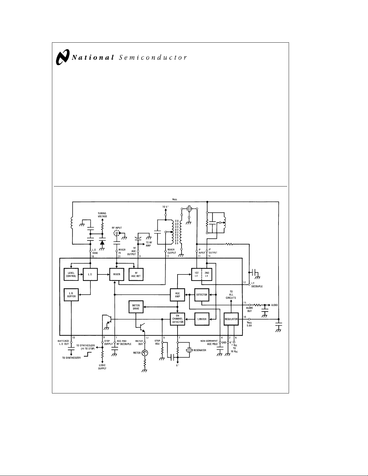
Block Diagram
May 1989
and sufficient gain are provided to allow the IC to also be
used in conjunction with a loopstick antenna.
Features
Y
Low supply current
Y
Level-controlled, low phase noise local oscillator
Y
Buffered local oscillator output
Y
Stop circuitry with adjustable stop threshold and adjustable stop window
Y
Open collector stop output
Y
Excellent THD and stop time performance
Y
Large amount of recovered audio
Y
RF AGC with open collector output
Y
Meter output
Y
Compatible with AM stereo
LM1863 AM Radio System for Electronically Tuned Radios
Order Number LM1863M
TL/H/5185– 1
See NS Package Number M20B
C
1995 National Semiconductor Corporation RRD-B30M115/Printed in U. S. A.
TL/H/5185
Page 2
Absolute Maximum Ratings
Supply Voltage 16V
Package Dissipation (Note 1) 1.7W
Storage Temperature Range
b
55§Ctoa150§C
Operating Temperature Range 0§Ctoa70§C
Soldering Information
Small Outline Package
Vapor Phase (60 sec) 215
Infrared (15 sec) 220
See AN-450 ‘‘Surface Mounting Methods and Their Effect
on Product Reliability’’ for other methods of soldering surface mount devices.
C
§
C
§
Electrical Characteristics
(Test Circuit, T
STATIC CHARACTERISTICS
Supply Current V
Pin 16, Regulator Voltage 5.6 V
Operating Voltage Range (See Note 2) 7 16 V
Pin 3 Leakage Current V
Pin 9, Low Output Voltage V
Pin 17, Output Voltage V
DYNAMIC CHARACTERISTICS: (f
Maximum Sensitivity VINFor V
20 dB Quieting Sensitivity VINfor 20 dB S/N in Audio 15 30 mV
Maximum Signal to Noise Ratio V
Total Harmonic Distortion V
Total Harmonic Distortion V
Audio Output Level V
Overload Distortion V
Meter Output Voltage V
Meter Output Voltage V
Local Oscillator Output Level (See Note 3), SW1ePosition 1
on Pin 19
Local Oscillator Output Level (See Note 3), SW1ePosition 2 125 mVrms
on Pin 19
Stop Detector Valid Station V
Frequency Window the two frequencies at which 2.5 4 5.5 kHz
Stop Detector Valid Station Find VINfor which Pin 9l1V,
Signal Level Threshold SW2
RF AGC Threshold Find VINthat produces
Pin 3 Low Output Level V
Pin 9 Leakage Current V
Pin 17 Output Resistance V
Note 1: Above T
Note 2: All data sheet specifications are for V
Note 3: The local oscillator level at Pin 19 is identical to the level at Pin 18 since Pin 19 is an emitter follower off of Pin 18.
e
25§C, Vae12V, SW1ePosition 1, SW2ePosition 2, unless indicated otherwise)
A
Parameter Conditions Min Typ Max Units
e
0 mV 8.3 12.5 mA
IN
e
0 mV 0.1 mA
IN
e
0 mV, SW2ePosition 1 .15 V
IN
e
0mV 0 V
IN
MOD
e
IN
IN
IN
IN
IN
IN
IN
1 kHz, f
e
e
e
e
e
e
e
e
1 MHz, Me0.3)
IN
e
6 mVrms 7.5 mV
AUDIO
10 mV 40 54 dB
10 mV .26 %
10 mV, Me0.8 .63 2 %
10 mV 80 120 160 mVrms
50 mV, Me0.8 7.5 %
100 mV 0.5 V
10 mV 4.6 V
100 147 mVrms
e
10 mV, difference between
IN
k
Pin 9
1V, SW2ePosition 1
81670mVrms
3 6 10 mVrms
e
25§C derate based on T
A
e
Position 1
10 mA of current into Pin 3
e
30 mV 0.1 V
IN
e
30 mV 0.1 mA
IN
e
10 mV 825 X
IN
e
150§C and i
j (MAX)
ae
12V and may change slightly with supply.
e
85§C/W.
jA
2
Page 3
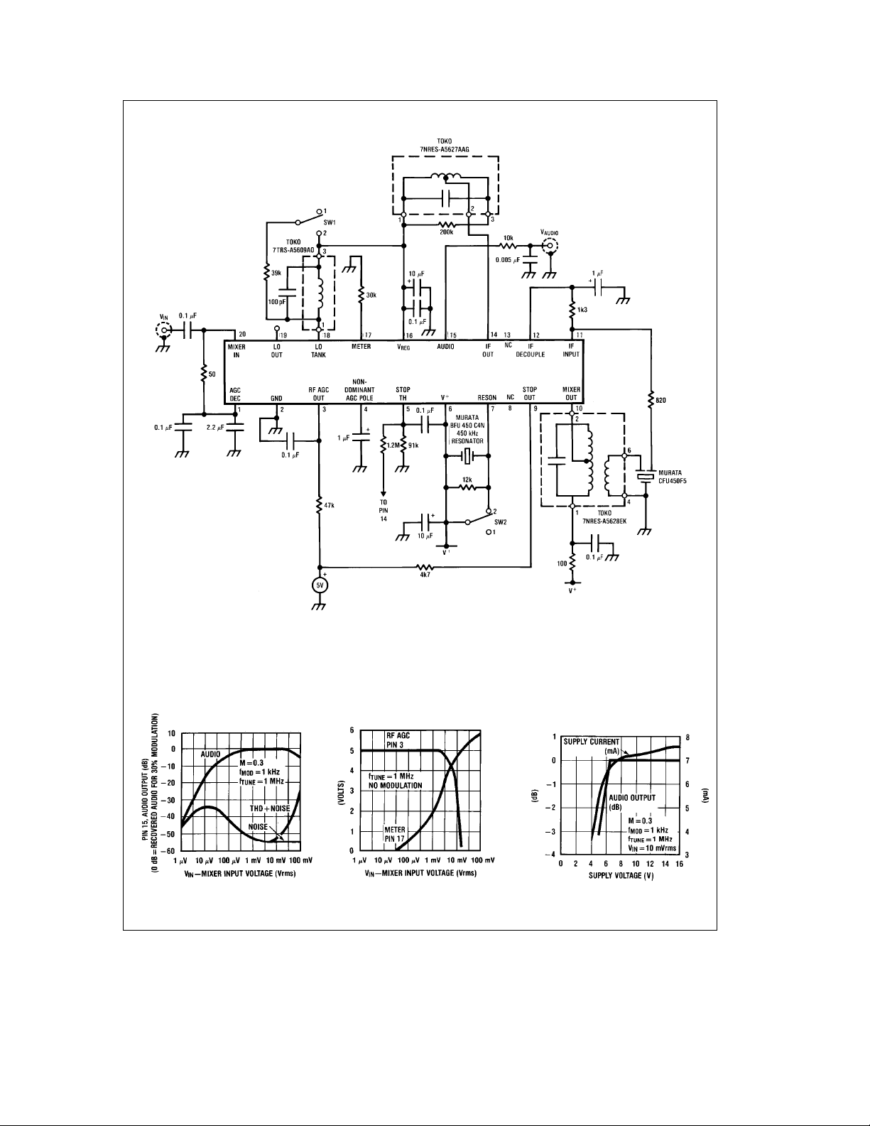
Test Circuit
Typical Performance Characteristics (From Test Circuit)
TL/H/5185– 9 TL/H/5185– 10 TL/H/5185– 11
3
TL/H/5185– 2
Page 4
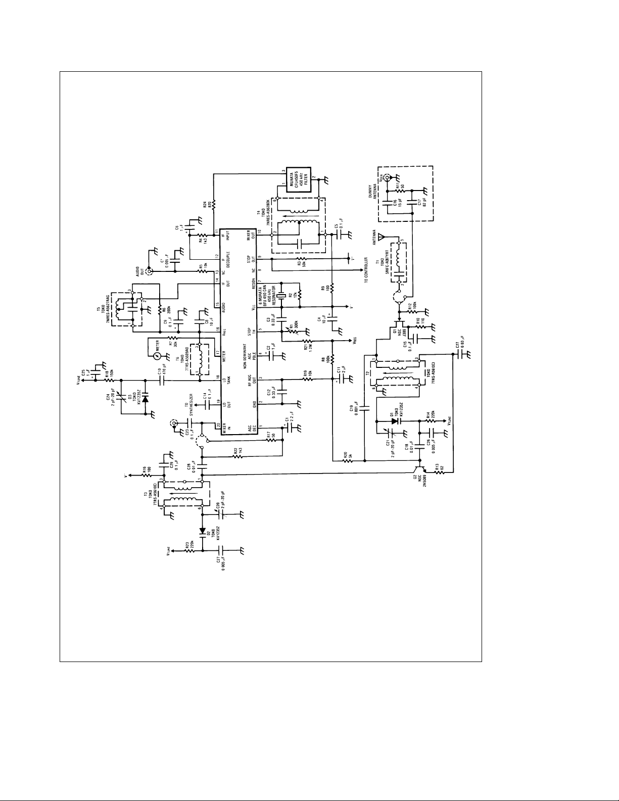
Application Circuit
TL/H/5185– 8
LM1863: AM ETR Radio
4
Page 5
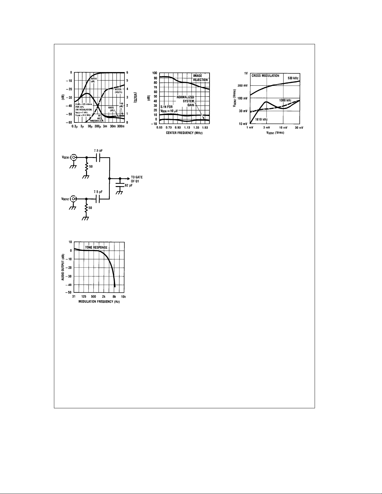
Performance Characteristics of Applications Circuit
TL/H/5185– 12
TL/H/5185– 13
TL/H/5185– 14
Cross modulation is
measured using the
following dummy antenna:
TL/H/5185– 15
TL/H/5185– 16
The following procedure was used to measure cross modulation:
1. Tune the radio to the center frequency of interest and tune V
2. Set at 0 dB audio reference with V
3. Remove the modulation from V
4. Set the modulation level of V
center frequency.
5. Increase the level of V
modulation measurement.
GEN2
,e10 mV RMS and 30% AM mod; f
GEN
and set the level of V
GEN1
GEN2
e
80% at f
MOD
e
1 kHz and tune V
untilb40 dB of audio is recovered. The level of V
, to this same frequency.
GEN
.
GEN1
GEN2
e
1 kHz.
MOD
g
40 kHz away from
is the cross
GEN2
Additional Performance Information:
* THD for 80% modulation for f
e
V
1V is 0.5%
GEN
e
V
10 mV is 0.4%
GEN
k
* Tweet
2% at all input levels.
* Typical time for valid stop indication
Note: Tweet is an audio tone produced by the 2nd and 3rd harmonic of the IF beating against the received
signal. It is measured as an equivalent modulation level: ie, 30% tweet has the same amplitude at the
detector as a desired signal with 30% modulation.
MOD
e
1 kHZ at:
k
50 ms.
5
Page 6

IC External Components (See Application Circuit)
Component Typical Value Comments
C1 2.2 mF Sets dominant AGC pole, affects stop time
C2 1 mF Sets non-dominant AGC pole, affects stop
C3 0.33 mF Stop level threshold decoupling, affects
C4 10 mF Supply decoupling, low frequency.
C5 0.1 mF Supply decoupling, high frequency.
C6 1 mF IF decouple, affects IF gain.
C7 0.005 mF Audio output filter, removes IF ripple from
C8 10 mF Regulator decouple, low frequency.
C9 0.1 mF Regulator decouple, high frequency.
C10 470 pF Pad capacitor for varactor, affects tracking.
C11 2 mF RF AGC decouple, affects stop time and
C12 0.33 mF RF AGC high frequency decouple.
C14 0.1 mF Local oscillator output coupling.
C19 0.001 mF Sets gain at high end of AM band.
C26 0.005 mF Sets gain at low end of AM band.
C28 0.01 mF Couples RF stage output to mixer input,
R1 300k Pot. Sets level stop threshold.
R2 12k Sets size of stop window.
R3 50k Open collector pull up resistor.
R4 1k3 IF filter termination, and gain set.
R5 10k Sets RC time constant on audio outputs,
R6 200k Sets gain of IF stage, affects noise floor and
R7 Meter Dependent Sets full-scale deflection of meter.
R8 100k Sets gain and threshold of RF AGC.
R9 100X Aids mixer output decoupling.
R19 10k Sets 2‘nd pole in RF AGC, affects THD for
R21 1.2 MX Biases pin 5 to 0.4 volts which permits
R24 820X Sets system gain.
D1, D2, D3, TOKO Varactor diodes.
Resonator 450 kHz
IF filter Murata* Sets selectivity and tone response.
KV1235Z or
Equivalent
g
1 kHz Parallel type resonator.
Murata*, BFU450C4N
CFU450F5
and THD.
time and THD.
stop time and sensitivity of stop detector to
large modulation peaks.
detector.
THD.
keep small to insure proper stop time
performance when RF AGC is active.
smaller values may cause distortion of high
frequencies.
sensitivity.
large input signals.
shorter stop time.
*Murata
2200 Lake Park Drive
Smyrna, GA 30080
(404) 436-1300
6
Page 7

Performance Characteristics of Applications Circuit (Continued)
Part No. 5MFC–A087YRT
TOKO
Center Frequencye2 MHz
l
Qu
50 at 2 MHz
Part No. 7NRES–A5628EK
TOKO
TL/H/5185– 17
Part No. 7TRS–A5610CI
TOKO
Qul95 at 1 MHz
e
L
200 mH
4–6
Part No. 7NRES–A5627AAG
TOKO
TL/H/5185– 18
*Toko America
1250 Feehanville Drive
Mount Prospect, IL 60056
(312) 297-0070
Center Frequencye450 kHz
l
Qu
100 at 450 kHz
TL/H/5185– 19
Part No. 7TRS–A5609A0
TOKO
Center Frequencye1 MHz
l
Qu
95 at 1 MHz
e
L
110 mH
1–3
7
Center Frequencye450 kHz
l
Qu
100 at 450 kHz
TL/H/5185– 21
TL/H/5185– 20
Page 8

Layout Considerations
Although the pinout of the LM1863 has been chosen to minimize layout problems, some care is required to insure proper performance. If the LM1863 is used with a loopstick antenna, care in the placement of C3 must be observed in
order to minimize tweet radiation. Orient C3 parallel to the
axis of the loopstick and as far away as possible. Keep C3
close to the IC. The ground on C6 should be located near
the ground terminal of the 450 kHz ceramic filter. C11
should be located near Q2 and C12 should be located near
the IC. Also, the resonator on Pin 7 and resistor R2 should
be located near the IC in order to minimize tweet radiation.
PC Layout (Component Side)
The mixer output, Pin 10 and the IF input, Pin 11, traces
should be as short as possible to prevent stray pick up from
the resonator.
Applications Information
(See typical application and LM1863 schematic diagram.)
STOP DETECTOR
There are two criteria that determine when an electronically
tuned radio is tuned to a valid station. The first criterion is
that the incoming signal be of sufficient strength to be listenable. The second criterion requires that the radio be tuned
TL/H/5185– 22
8
Page 9

Applications Information (Continued)
to the center frequency of the incoming station. Both the
signal strength threshold and the center tune window are
externally adjustable.
The signal strength threshold is set by resistor R1. Increasing the value of this resistor will reduce the signal level
threshold. There is no difficulty in setting the signal strength
threshold, either above or below the AGC threshold.
Resistor R2 sets the center tune window. The incoming station is considered to be center tuned whenever the frequency of the signal at the IF output falls within the center tune
window. Increasing the value of R2 will narrow the window,
while decreasing R2 will widen the window. Since there is
some interaction between R2 and R1, R2 should be chosen
before R1. In the United States, stations within the AM band
are spaced no closer than 10 kHz apart. Consequently, the
controller should be set up to stop every 10 kHz within the
AM band when the ETR is in scan mode. A center tune
window anywhere less than
in determining the center tune condition, though a narrower
stop window is desirable in order to minimize the chance
that side bands from a strong adjacent channel will fall within the stop window.
Because of asymmetry in the resonator amplitude characteristic, the center tune stop window will not be symmetric
about the center frequency of the resonator. This is not a
problem as long as the stop window brackets the center
frequency of the IF and does not extend into the next channel. However, in order to avoid any problems in this regard it
is recommended that the resonator center frequency deviate no more than
IF.
The stop output, Pin 9, is an open collector NPN transistor.
This output must be taken to a positive voltage through a
load resistor, R3. A valid stop condition is indicated by a
high output level on Pin 9 (i.e., the NPN is turned off). The
voltage on this pin should not exceed 16 volts.
STOP DETECTOR STOP TIME
The amount of time required for the LM1863 to output an
accurate stop indication on Pin 9 is defined as the stop time.
The stop time determines how quickly the ETR can scan
across the AM band. There are several factors that influence the stop time. Since the signal level stop function operates in conjunction with the Automatic Gain Control
(AGC), the AGC settling time is a critical factor. This settling
time is dominated by the low frequency AGC pole which is
set by C1 and internal IC resistances. Decreasing C1 will
decrease the AGC settling time but increase total harmonic
distortion, THD, of the recovered audio. A good compromise
between AGC settling time and THD is very difficult to reach
with a single pole AGC system. Consequently, the LM1863
has been designed with a second, higher frequency, AGC
pole. This non-dominant pole is externally set by capacitor
C2. As a result, C1 can be made much smaller than it otherwise could for an equivalent amount of THD. Reducing C1
will reduce the stop time. The combination of C1 and C2 as
shown in the applications circuit results in a stop time of less
than 50 ms for most input conditions, while at the same time
the circuit achieves .9% THD at 80% modulation with 400
Hz modulation frequency at 10 mV input signal strength.
Had C2 not been present the stop time would still be 50 ms
but the THD for similar input conditions would be 8%. By
decreasing both C1 and C2 (keeping the ratio of C1/C2
constant) the stop time can be reduced at the expense of
THD, while the converse is also true.
g
g
10 kHz is therefore adequate
1 kHz from the center frequency of the
The addition of a second pole to the AGC response does
add some ringing to the AGC voltage following signal transients. The frequency, duration and amount of ringing are
dependent on where both AGC poles are placed and to
some extent the input signal conditions. The amount of ringing should be kept to a minimum in order to insure proper
stop indications. The amount of ringing can be reduced by
either reducing C2 (this will increase THD) or by increasing
C1 (this will improve THD but increase stop time).
If the ratio of C1/C2 is made too small, an increase in low
frequency noise may be noticed resulting from the peaking
that a closed loop two pole system exhibits near the unity
gain frequency. The extent of this peaking can be observed
by examining the amount of recovered audio at various low
frequency modulations. In general, the values shown reach
a good compromise between THD, stop time, ringing and
low frequency noise.
The center tuning detector on the LM1863 passes the signal at the IF output through a limiting amplifier which removes most of the modulation from the IF waveform. The
output of this limiter is then applied to the resonator on Pin
7. Unfortunately, large modulation peaks are not completely
removed by the limiting amplifier. Without C3, these large
modulation peaks would cause glitches on the stop output
when the LM1863 was tuned to a valid station. C3 acts to
reduce these glitches by filtering the output of the center
tune circuit. C3, however, also affects the stop time and
cannot be made arbitrarily large. A time constant of about
30 ms on Pin 5 gives the best compromise. R21 biases Pin
5 to about .4 volts, which is below the stop threshold at this
point. This biasing results in a shorter stop time.
Extra precaution can be taken within the software of the
controller IC to further insure accurate stop detector performance over a wide variety of input signal conditions. A
typical controller IC stop algorithm is as follows:
The controller waits the first 10 ms after the LM1863 is
tuned to the next channel. The controller then samples
the LM1863 stop output 10 times within the next 40 ms.
If no high output is sensed within that time the controller concludes there is no valid station at the frequency
and moves to the next channel. If, however, at least
one high output is detected within the first 50 ms the
controller waits an additional 200 ms and at the end of
that time re-samples the stop output in order to make
its final stop determination.
RF AGC
The RF AGC detector is designed to control the gain of an
external RF amplifier which is placed between the antenna
and the mixer input. The RF AGC operates by detecting
when the input signal to the mixer reaches 6 mVrms, the RF
AGC threshold. When the mixer input signal reaches this
level the RF AGC is activated and will hold the mixer input
level relatively constant at the level of the RF AGC threshold. The gain of the RF AGC determines how constant the
RF AGC can control the RF output. The LM1863 RF AGC is
high gain and consequently the RF AGC output, Pin 3, will
transition from high to low over a very narrow input range to
the mixer when the LM1863 is examined in an OPEN LOOP
condition. However, in a radio where the RF AGC controls
the RF gain, a CLOSED LOOP negative feedback system is
established. In this application the RF AGC output will transition from high to low over a large range of signal levels to
the input of the RF stage.
9
Page 10

Applications Information (Continued)
The RF AGC threshold has been carefully chosen to prevent overloading the mixer, which would cause distortion
and tweet problems. However, the threshold level is sufficiently large to minimize the possibility of strong adjacent
stations de-sensitizing the radio by activating the RF AGC
and thereby gain reducing the RF front end.
The RF AGC output, Pin 3, is an open collector NPN transistor. This collector must be tied to a positive voltage through
a load resistor, R8. Furthermore, decoupling is required
(C11 and C12) in order to insure that the RF AGC does not
induce significant distortion in the recovered audio. However, the tradeoff between good THD performance and fast
stop time is not too severe for the RF AGC because large
changes in the RF AGC level are unlikely when moving between adjacent channels. This is because the selectivity in
the RF stage is not great enough to cause abrupt signal
level changes at the mixer input as the radio is tuned. Thus,
since the RF AGC does not have to follow abrupt signal
level changes, the time constant on the AGC output can be
relatively long which allows for good THD performance. C12
is required in order to insure good RF decoupling of signals
at the RF AGC output, and sets the non-dominant pole.
The RF AGC 10 mA threshold is fixed at 6 mVrms at the
mixer input. However, due to the gain of the RF stage and
losses through the RF transformers, this level may be different when referenced to the antenna input. For the application circuit shown the RF threshold occurs at 2 mVrms at
the dummy antenna input. Thus, the RF AGC threshold can
effectively be adjusted by altering the gain of the RF stage.
The value of R8 also has some affect on the RF AGC
threshold of the application circuit. Smaller values will tend
to increase the threshold while larger values will tend to
reduce the threshold.
GAIN DISTRIBUTION
The purpose of this section is to clarify some of the tradeoffs involved in redistributing gain from one portion of the
radio to another. An AM radio basically has three gain
blocks consisting of the RF stage, the mixer, and the IF
stage. The total gain of these three blocks must be sufficiently large as to insure reception of weak stations. Given
then a fixed amount of required gain how does distributing
this gain among the three blocks affect the radio performance?
Large amounts of gain in the RF stage will have the effect of
decreasing the RF AGC threshold. A decreased RF AGC
threshold means that it is more likely that strong adjacent
stations can activate the RF AGC and desensitize the radio.
Also, a lot of RF gain implies large signals across the RF
varactor diodes, which is undesirable for good tracking and
can result in overloading these varactors which can cause
cross modulation. On the other hand, high RF gain insures
good noise performance and improved THD.
High mixer gain implies large signal swings at the mixer output, especially on AGC transients. These large signal
swings could cause the mixer ouput transistors to saturate
and also could overload the IF stage. On the other hand,
redistributing the gain from the IF to the mixer would improve the noise performance of the radio. The gain of the
mixer can be controlled moving the tap on the mixer output
transformer, T4.
Since the output signal level of the IF is held constant by the
AGC, increasing gain in the IF has the effect of reducing the
signal level at the IF input. Noise sources at the IF input
therefore become a larger percentage of the IF input signal
thereby degrading the S/N floor of the radio. For this reason, the LM1863 employs 20 dB of IF AGC. The IF gain of
the LM1863 is adjustable by changing the tap across the IF
ouput coil, or by changing the ratio of R24 to R4.
The gain distribution for the application circuit is as follows:
Gain Distribution
e
V
0 dB (10 mV)
G
eb
16 dB
V1
ea
10 dB (Pin 20)
V2
ea
33 dB (Pin 11)
V3
ea
84 dB (Pin 14)
V
O
TL/H/5185– 23
The IF gain could also be varied by changing the value of
R6 across the IF output coil. However, it is a good idea to
maintain a high Q IF tank in order to achieve good adjacent
channel rejection. In order to prevent distortion due to overloading the IF amplifier, it is important that the impedance
Pin 14 sees looking into the IF output tank, T5, does not go
below 3K ohms.
The above gain distribution is prior to any AGC action in the
radio. This distribution represents a good compromise between the various tradeoffs outlined previously.
LEVEL CONTROLLED LOCAL OSCILLATOR
Tracking of the RF varactors with the local oscillator varactor is a serious consideration in order to insure adequate
performance of the ETR radio. Due to non-linear capacitance versus voltage characteristic of the varactor, large
signals across these varactors will tend to modulate their
capacitance and cause tracking problems. This problem is
compounded further if the level of the signals across the
varactors change. In an AM radio, the local oscillator frequency changes a ratio of two to one. The Q of the oscillator tank remains fairly constant over this range. Thus, since
e
Q
RP/0LeConstant, this implies that RP(R
loaded parallel resistance of the tank) must change two to
e
un-
P
one. The internal level-control loop prevents the two to one
change in AC voltage across the tank which the change in
the R
would otherwise cause.
P
Phase jitter of the local oscillator is very important in regard
to AM stereo, where L-R information is contained in the
phase of the carrier. Local oscillator jitter has the effect of
modulating the L-R channel with phase noise, thus degrading the stereo signal to noise performance. Great care has
been taken in the design of the LM1863 local oscillator to
insure that phase jitter is a minimum. In fact the dominant
source of phase jitter is the high impedance resistor drive to
the varactor. The thermal noise of the resistor modulates
the varactor voltage, thus causing phase jitter.
VARACTOR TUNED RF STAGE
Electronically tuned car radios require the use of a tuned RF
stage prior to the mixer. Many of the performance charac-
10
Page 11

Applications Information (Continued)
teristics of the radio are determined by the design of this
stage. Generally speaking it is very difficult to design an
integrated RF stage in bipolar, as bipolar transistors do not
have good overload characteristics. Thus, the RF stage is
usually designed using discrete components. Because of
this there is a great deal of concern with minimizing the
number of discrete components without severely sacrificing
performance. The applications circuit RF stage does just
this.
The circuit consists of only two active devices, an N-channel JFET, Q1, which is connected in a cascode type of configuration with an NPN BJT, Q2. Both Q1 and Q2 are varactor tuned gain stages. Q2 also serves to gain reduce Q1
when Q2’s base is pulled low by the RF AGC circuit on the
LM1863. The gain reduction occurs because Q1 is driven
into a low gain resistive region as its drain voltage is reduced. R10 and C15 set the gain of the 1’st RF stage which
is kept high (about 19 dB) for good low signal, signal/noise
performance. The gain of the front end to the mixer input
referenced to the generator output is about
T2 in conjunction with D1, C21 and C26 form the 1’st tuned
circuit. C26 does not completely de-couple the RF signal at
the cathode of the varactor. In fact, the combination of C26
and C19 act to keep the gain of the whole RF stage constant over the entire AM band. Without special care in this
regard the gain variation could be as high as 14 dB. This gain
variation would result from the increase in impedance at the
secondary’s of T2 and T1 as the tuned frequency is increased. The increased impedance results from a constant
e
Q
Rp/(wL) of the tanks over the AM band. With C26 and
C19 the gain is held constant to within 6 dB (including the
tracking error) over the entire AM band.
C27 de-couples RF signal from the top of T2’s primary and
allows Q2 to operate properly. C18 is a coupling capacitor
which in conjunction with C19 couples the signal from the
1’st RF stage to the 2’nd RF stage. R20 acts to isolate this
signal from AC ground at C11. R19 acts in conjunction with
C12 to set a high frequency (ie: non-dominant) RF AGC
pole which is important for low distortion when the RF AGC
is active. The dominant RF AGC pole is set by R8 and C11.
Q2 is a high beta transistor allowing for little voltage drop
across R20 and R8 due to base current. This keeps the
emitter of Q2 sufficiently high (in the absence of RF AGC) to
bias Q1 in its square law region.
R13 acts to reduce the 2’nd stage gain and increase Q2’s
signal handling. R13 must not get too large, however, (ie:
l
R13
100 X), or low level signal/noise will be degraded. T3
in conjunction with C20, C27 and D2 form the 2’nd RF tuned
circuit. The output of Q2 is capacitively coupled through C28
to the mixer input. The output of Q2 is loaded not only by
the reflected secondary impedance but also by R22. R22 is
carefully chosen to load the 2’nd stage tuned circuit and
broaden its bandwidth. The increased bandwidth of the 2’nd
stage greatly improves the cross modulation performance of
the front end. In the absence of this increased bandwidth,
the relatively large AC signals across varactor D2 result in
cross modulation. R22 also reduces the total gain of the
2’nd stage. R22 does slightly degrade (by about 6 dB) the
image rejection especially at the high end of the AM band.
However, the image rejection of this front end is still excellent and 6 dB is a small price to pay for the greatly increased
immunity to cross modulation.
R16 and C29 decouple unwanted signals on V
coupled into the RF stage. This front end also offers superi-
a
a
10 dB.
from being
or performance with respect to varactor overload by strong
adjacent channels. This results because of the way that
gain has been distributed between the 1’st and 2’nd stages.
In summary, this front end offers two stages of RF gain with
the 2’nd stage acting to gain reduce the 1’st stage when RF
AGC is active. Furthermore, a unique coupling scheme is
employed from the output of the 1’st stage to the input of
the 2’nd stage. This coupling scheme equalizes the gain
from one end of the AM band to the other. Additional care
has been taken to insure that excellent cross modulation
performance, image rejection, signal to noise performance,
overload performance, and low distortion are achieved. Performance characteristics for this front end in conjunction
with the LM1863 are shown in the data sheet. Also, information with regard to the bandwidth of the front end versus
tuned frequency are given below.
TUNED FREQUENCY
530 kHz 6.6 kHz
600 kHz 7.2 kHz
1200 kHz 20.6 kHz
1500 kHz 26.4 kHz
1630 kHz 36 kHz
VARACTOR ALIGNMENT PROCEDURE
The following is a procedure which will allow you to properly
align the RF and local oscillator trim capacitors and coils to
insure proper tracking across the AM band.
1. Set the voltage across the varactors
2. Set the trimmers to 50%.
3. Adjust the oscillator coil until the local oscillator is at 980
kHz.
4. Increase the varactor voltage until the local oscillator
(L0) is at 2060 kHz and check to see if this voltage is less
than 9.5 volts but greater than 7.5 volts. If it is then the
L0 is aligned. If it is not then adjust the L0 coil/trimmer
until the varactor voltage falls in this range.
5. Set the RF in to 600 kHz and adjust the tuning voltage
until the L0 is at 1050 kHz. Peak all RF coils for maximum recovered audio at low input levels.
6. Set RF in to 1500 kHz and adjust the tuning voltage until
the L0 is at 1950 kHz. Peak all RF trim capacitors for
maximum recovered audio at low input levels.
7. Go back to step 5 and iterate for best adjustment.
8. Check the radio gain at 530 kHz and 750 kHz to make
sure that the gain is about the same at these two frequencys. If it is not, then slightly adjust the RF coils until
it is.
The above procedure will insure perfect tracking at 600 kHz,
950 kHz and 1500 kHz. The amount of gain variation across
the AM band using the above procedure should not exceed
6 dB.
ADDITIONAL INFORMATION
R5 and C7 act as a low pass filter to remove most of the
residual 450 kHz IF signal from the audio output. Some residual 450 kHz signal is still present, however, and may
need to be further removed prior to audio amplification. This
need becomes more important when the LM1863 is used in
conjunction with a loopstick antenna which might pick up an
amplified 450 kHz signal. An additional pole can be added
to the audio output after R5 and C7 prior to audio amplification if further reduction of the 450 kHz component is required.
b
3 dB BANDWIDTH
e
1 volt.
11
Page 12

Equivalent Schematic Diagram
TL/H/5185– 24
12
Page 13

13
Page 14

Physical Dimensions inches (millimeters)
Plastic Small Outline Package (M)
Order Number LM1863M
NS Package Number M20B
LM1863 AM Radio System for Electronically Tuned Radios
LIFE SUPPORT POLICY
NATIONAL’S PRODUCTS ARE NOT AUTHORIZED FOR USE AS CRITICAL COMPONENTS IN LIFE SUPPORT
DEVICES OR SYSTEMS WITHOUT THE EXPRESS WRITTEN APPROVAL OF THE PRESIDENT OF NATIONAL
SEMICONDUCTOR CORPORATION. As used herein:
1. Life support devices or systems are devices or 2. A critical component is any component of a life
systems which, (a) are intended for surgical implant support device or system whose failure to perform can
into the body, or (b) support or sustain life, and whose be reasonably expected to cause the failure of the life
failure to perform, when properly used in accordance support device or system, or to affect its safety or
with instructions for use provided in the labeling, can effectiveness.
be reasonably expected to result in a significant injury
to the user.
National Semiconductor National Semiconductor National Semiconductor National Semiconductor
Corporation Europe Hong Kong Ltd. Japan Ltd.
1111 West Bardin Road Fax: (
Arlington, TX 76017 Email: cnjwge@tevm2.nsc.com Ocean Centre, 5 Canton Rd. Fax: 81-043-299-2408
Tel: 1(800) 272-9959 Deutsch Tel: (
Fax: 1(800) 737-7018 English Tel: (
National does not assume any responsibility for use of any circuitry described, no circuit patent licenses are implied and National reserves the right at any time without notice to change said circuitry and specifications.
Fran3ais Tel: (
Italiano Tel: (
a
49) 0-180-530 85 86 13th Floor, Straight Block, Tel: 81-043-299-2309
a
49) 0-180-530 85 85 Tsimshatsui, Kowloon
a
49) 0-180-532 78 32 Hong Kong
a
49) 0-180-532 93 58 Tel: (852) 2737-1600
a
49) 0-180-534 16 80 Fax: (852) 2736-9960
 Loading...