

Page 1
LM18298 Dual Full-Bridge Driver
LM18298 Dual Full-Bridge Driver
April 1992
General Description
The LM18298 is a high voltage, high current dual full-bridge
driver designed to accept standard TTL logic levels and
drive inductive loads such as relays, solenoids, DC and
stepping motors. Two enable inputs are provided to gate the
input control signals.
The emitters of the lower transistors of each bridge are connected together and the corresponding external terminal
can be used for the connection of a current sensing resistor.
An additional supply input is provided to accommodate conventional logic supply voltages.
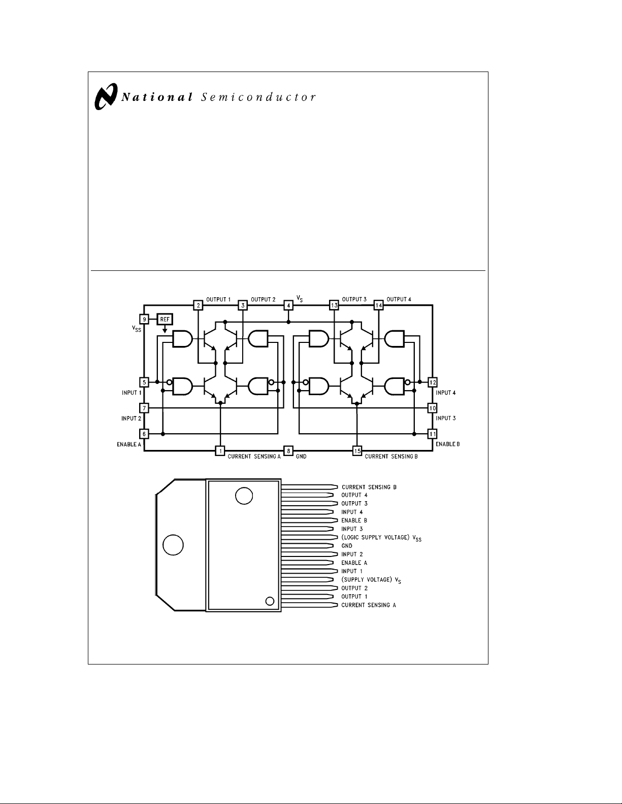
Block & Connection Diagrams
Features
Y
Power supply voltage up to 46V
Y
2A output per channel
Y
Low saturation voltage
Y
Thermal shutdown protection
Y
Logical ‘‘0’’ input voltage up to 1.5V
(High noise immunity)
Y
Pin for pin replacement for L298N
Applications
Y
DC and stepper motor drivers
Y
Relay and solenoid drivers
TL/H/9302– 1
TL/H/9302– 2
TO 220-15
Order Number LM18298T
NS Package Number TA15A
C
1995 National Semiconductor Corporation RRD-B30M115/Printed in U. S. A.
TL/H/9302
Page 2
Absolute Maximum Ratings (Note 1)
If Military/Aerospace specified devices are required,
please contact the National Semiconductor Sales
Office/Distributors for availability and specifications.
Main Supply (Pin 4) 50V
Logic Supply (Pin 9) 7V
Logic Inputs
(Pins 5, 6, 7, 10, 11, 12)
Peak Output Current (Per Channel)
Non-Repetitive (t
Repetitive (80% duty cycle, t
DC Operation 2A
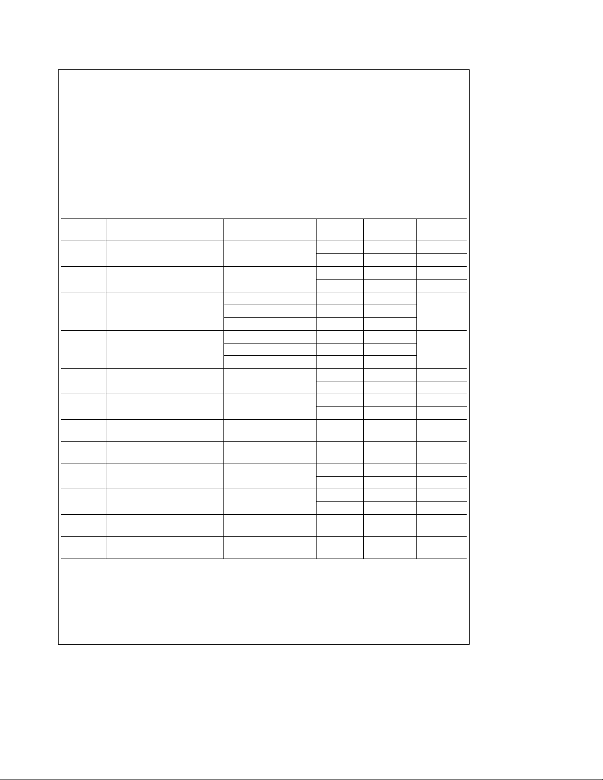
Electrical Characteristics
e
V
42V, V
S
e
100 ms) 3A
e
5V, I
SS
O
e
10 ms) 2.5A
ON
e
0A, T
e
J
b
0.3 to 7V
25§C, Le0V, He5V, unless otherwise specified
Symbol Parameter Conditions
V
S
V
SS
I
S
Main Supply Voltage (Pin 4) V
Logic Supply Voltage (Pin 9) 4.5 V (min)
Main Supply Quiescent Current EnableeH, InputeL9 22
(Pin 4)
EnableeH, InputeH 32 70 mA (max)
EnableeL, InputeX4
I
SS
Logic Supply Quiescent Current EnableeH, InputeL22 36
(Pin 9)
EnableeH, InputeH 6 12 mA (max)
EnableeL, InputeX6
V
IL
V
IH
I
IL
I
IH
V
EN L
V
EN H
I
EN L
I
EN H
Low Level Input Voltage
(Pins 5, 7, 10, 12)
High Level Input Voltage 2.3 V (min)
(Pins 5, 7, 10, 12)
Low Level Input Current InputeL
(Pins 5, 7, 10, 12)
High Level Input Current InputeH 30 100
(Pins 5, 7, 10, 12)
Low Level Enable Voltage
(Pins 6, 11)
High Level Enable Voltage 2.3 V (min)
(Pins 6, 11)
Low Level Enable Input Current EnableeL
(Pins 6, 11)
High Level Enable Input Current EnableeH
(Pins 6, 11)
Sense Voltage (Pins 1, 15)
Power Dissipation (Note 2) 25W
ESD Susceptibility (Note 3) 1 kV
Lead Temperature (Soldering, 10 seconds) 260§C
Storage Temperature Range
Operating Ratings
Junction Temperature Range (TJ)
Main Supply (Pin 4) 46V
b
1toa2.3V
b
65§Ctoa150§C
b
40§Ctoa150§C
Typical Limit Units
(Note 4) (Note 5) (Limits)
a
2.5 V (min)
SS
46 V (max)
7 V (max)
b
0.3 V (min)
1.5 V (max)
V
SS
b
10 mA (max)
V (max)
mA (max)
b
0.3 V (min)
1.5 V (max)
V
SS
b
10 mA (max)
V (max)
30 100 mA (max)
2
Page 3

Electrical Characteristics (Continued)
e
V
S
Symbol Parameter Conditions
V
CE sat (H)
V
CE sat (L)
V
CE sat
V
sense
42V, V
e
SS
5V, I
e
O
0A, T
e
25§C, unless otherwise specified
J
Source Saturation Voltage I
(Pins 2, 3, 13, 14)
Sink Saturation Voltage I
(Pins 2, 3, 13, 14)
Total Drop I
CE sat (H)
a
V
CE sat (L)
V
Sensing Voltage (Pins 1, 15) ts50 ms
Typical Limit Units
(Note 4) (Note 5) (Limits)
e
1A 1.35 1.7
O
e
I
2A 2.0 2.7
O
e
1A 1.2 1.6
O
e
I
2A 1.7 2.3
O
e
1A 3.2
O
e
I
2A 4.9
O
Continuous
V (max)
V (max)
V (max)
b
1
b
0.5
V (min)
Continuous 2 V (max)
T
1
T
2
T
3
T
4
T
5
T
6
T
7
T
8
f
C
Note 1: Absolute Maximum Ratings indicate limits beyond which damage to the device may occur. DC and AC electrical specifications do not apply when
operating the device beyond its specified Operating Ratings.
Note 2: The maximum power dissipation must be derated at elevated temperatures and is a function of T
dissipation at any temperature is P
case thermal resistance (i
Note 3: Human body model, 100 pF discharged through a 1.5 kX resistor.
Note 4: Typicals are at 25
Note 5: Limits are guaranteed and 100% tested.
Source Current Turn-Off Delay 0.5 Input to 0.9 IO(
Source Current Fall Time 0.9 IOto 0.1 IO(
Figure 2
Source Current Turn-On Delay 0.5 Input to 0.1 IO(
Source Current Rise Time 0.1 IOto 0.9 IO(
Figure 2
Sink Current Turn-Off Delay 0.5 Input to 0.9 IO(
Sink Current Fall Time 0.9 IOto 0.1 IO(
Figure 3
Sink Current Turn-On Delay 0.5 Input to 0.1 IO(
Sink Current Rise Time 0.1 IOto 0.9 IO(
Commutation Frequency I
e
b
(T
D max
) of the LM18298 is 3§C/W.
JC
C and represent the most likely parametric norm.
§
TC)/iJCor the number given in the Absolute Maximum Ratings, whichever is lower. The typical junction-to-
J max
e
2A 25 kHz
O
Figure 3
Figure 2
) 0.5 ms
) 0.15 ms
Figure 2
) 1.3 ms
) 0.85 ms
Figure 3
) 0.25 ms
) 0.1 ms
Figure 3
) 1.3 ms
) 0.1 ms
, iJC, and TC. The maximum allowable power
J max
3
Page 4

Typical Performance Characteristics
Output Voltage
(See
Figure 1
)
Source Current
Switching Times
Output Voltage
(See
Figure 1
)
Source Current
Switching Times
Maximum Power Dissipation
TL/H/9302– 3
Main Supply Quiescent
Current (IS, Pin 4)
Sink Current
Switching Times
Sink Current
Switching Times
4
TL/H/9302– 12
Logic Supply Quiescent
Current (ISS, Pin 9)
TL/H/9302– 13
Page 5

Test Circuits
TL/H/9302– 5
FIGURE 2(a). Source Current
Switching Time Test Circuit
FIGURE 1. Input/Enable Threshold Test Circuit
TL/H/9302– 4
TL/H/9302– 6
FIGURE 2(b). Source Current
Switching Time Definitions
TL/H/9302– 7
FIGURE 3(a). Sink Current
Switching Time Test Circuit
FIGURE 3(b). Sink Current Switching Time Definitions
TL/H/9302– 8
5
Page 6

Applications Information
TL/H/9302– 9
Enable B Inputs Motor Direction
Input 3eH, Input 4eL Clockwise
H Input 3eL, Input 4eH Counterclockwise
Input 3eInput 4 Dynamic Braking
L Input 3eX, Input 4eInput 3 Coast to a Stop
LeLow HeHigh Xedon’t care
FIGURE 4. Bidirectional DC Motor Control
TL/H/9302– 10
Enable B Input 3 Motor 1 Input 4 Motor 2
H H Dynamic Braking H Run
H L Run L Dynamic Braking
L X Coast to a Stop X Coast to a Stop
LeLow HeHigh XeDon’t Care
FIGURE 5. 2-Motor Controller
(Using both High- and Low-Side Driver Modes)
FIGURE 6. Two-Phase Bipolar Stepper Motor Control Circuit
CLAMP DIODES
When driving inductive loads, diodes are necessary to
clamp spikes at the LM18298 outputs. Clamp diodes must
have a recovery time of 200 ns or better and a forward drop
TL/H/9302– 11
of 1.2V or less at the rated load current. Typical devices are
the MB346 (Microsemi Corp., Santa Ana, CA), and the
V331X (Varo Semiconductor Inc., Garland, TX).
6
Page 7

7
Page 8

Physical Dimensions inches (millimeters)
LM18298 Dual Full-Bridge Driver
Order Number LM18298T
See NS Package Number TA15A
LIFE SUPPORT POLICY
NATIONAL’S PRODUCTS ARE NOT AUTHORIZED FOR USE AS CRITICAL COMPONENTS IN LIFE SUPPORT
DEVICES OR SYSTEMS WITHOUT THE EXPRESS WRITTEN APPROVAL OF THE PRESIDENT OF NATIONAL
SEMICONDUCTOR CORPORATION. As used herein:
1. Life support devices or systems are devices or 2. A critical component is any component of a life
systems which, (a) are intended for surgical implant support device or system whose failure to perform can
into the body, or (b) support or sustain life, and whose be reasonably expected to cause the failure of the life
failure to perform, when properly used in accordance support device or system, or to affect its safety or
with instructions for use provided in the labeling, can effectiveness.
be reasonably expected to result in a significant injury
to the user.
National Semiconductor National Semiconductor National Semiconductor National Semiconductor
Corporation Europe Hong Kong Ltd. Japan Ltd.
1111 West Bardin Road Fax: (
Arlington, TX 76017 Email: cnjwge@tevm2.nsc.com Ocean Centre, 5 Canton Rd. Fax: 81-043-299-2408
Tel: 1(800) 272-9959 Deutsch Tel: (
Fax: 1(800) 737-7018 English Tel: (
National does not assume any responsibility for use of any circuitry described, no circuit patent licenses are implied and National reserves the right at any time without notice to change said circuitry and specifications.
Fran3ais Tel: (
Italiano Tel: (
a
49) 0-180-530 85 86 13th Floor, Straight Block, Tel: 81-043-299-2309
a
49) 0-180-530 85 85 Tsimshatsui, Kowloon
a
49) 0-180-532 78 32 Hong Kong
a
49) 0-180-532 93 58 Tel: (852) 2737-1600
a
49) 0-180-534 16 80 Fax: (852) 2736-9960
 Loading...