

Page 1
LM1818 Electronically Switched Audio Tape System
LM1818 Electronically Switched Audio Tape System
April 1987
General Description
The LM1818 is a linear integrated circuit containing all of the
active electronics necessary for building a tape recorder
deck (excluding the bias oscillator). The electronic functions
on the chip include: a microphone and playback preamplifier, record and playback amplifiers, a meter driving circuit,
and an automatic input level control circuit. The IC features
complete internal electronic switching between the record
and playback modes of operation. The multipole switch
used in previous systems to switch between record and
playback modes is replaced by a single pole switch, thereby
allowing for more flexibility and reliability in the recorder design.*
*Monaural operation,
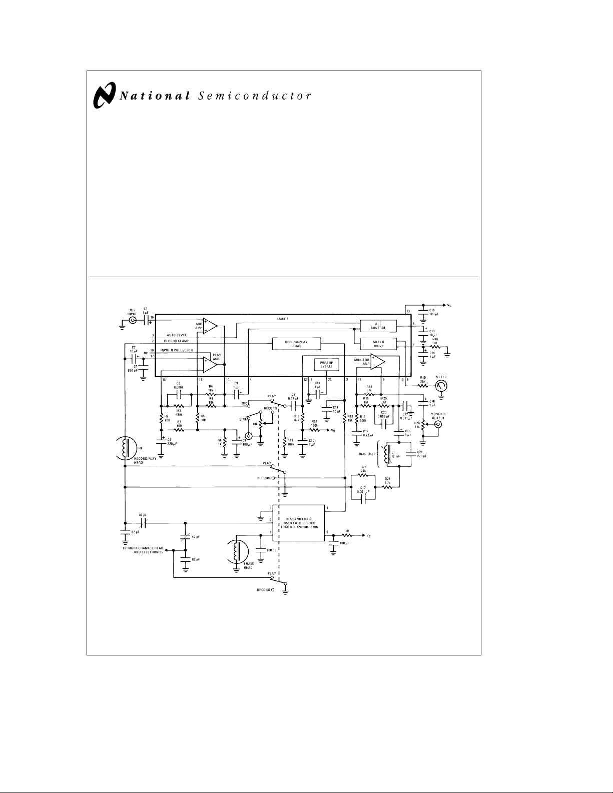
Figure 9
.
Typical Applications
Features
Y
Electronic record/play switching
Y
85 dB power supply rejection
Y
Motional peak level meter circuitry
Y
Low noise preamplifier circuitry
Y
3.5V to 18V supply operation
Y
Provision for external low noise input transistor
FIGURE 1. Stereo Application Circuit (Left Channel Shown), V
e
15V
S
TL/H/7894– 1
Order Number LM1818N
See NS Package Number N20A
C
1995 National Semiconductor Corporation RRD-B30M115/Printed in U. S. A.
TL/H/7894
Page 2
Absolute Maximum Ratings
If Military/Aerospace specified devices are required,
please contact the National Semiconductor Sales
Office/Distributors for availability and specifications.
Supply Voltage 18V
Package Dissipation, (Note 1) 1560 mW
Storage Temperature
b
65§Ctoa150§C
Operating Temperature 0
Ctoa70§C
§
Junction Temperature 150§C
Minimum Voltage on Any Pin
Maximum Voltage on Pins 2 and 5 0.1 V
Maximum Current Out of Pin 14 5 mA
b
0.1 V
DC
DC
DC
Lead Temperature (Soldering, 10 sec.) 260§C
Electrical Characteristics V
CC
e
6V, T
e
25§C, See Test Circuits
A
(Figures 2
and
3)
Parameter Conditions Min Typ Max Units
Operating Supply Voltage Range 3.5 18 V
Supply Current Test Circuit
(Figure 2)
512 mA
DC
Turn-ON Time Externally Programmable 50 400 ms
Playback Signal to Noise DIN Eq. (3180 and 120 ms), 20 –20 kHz,
e
R
0, Unweighted, V
S
at 400 Hz
Record Signal to Noise Flat Gain, 20–20 kHz, R
ALC OFF, V
at 1 kHz, Unweighted
REF
e
e
1mV 74 dB
REF
e
0,
S
1mV 69 dB
Fast Turn-ON Charging Current Pins 16 and 17 200 mA
Record and Playback Preamplifier fe100 Hz
Open Loop Voltage Gain
100 dB
Preamplifier Input Impedance Pin 16 or Pin 17 50 kX
Preamplifier Input Referred PSRR 1 kHz Ð Flat Gain 85 dB
Bias Voltage on Pin 18 in Play Mode
or Pin 15 in Record Mode
Monitor Amplifier Input Pins 11 and 12
Bias Current
Monitor Amplifier Open Record or Playback, fe100 Hz
Loop Voltage Gain
0.5 V
0.5 mA
80 dB
Monitor Output Current Capability Pins 9 and 10, Source Current Available 400 750 mA
Monitor Amplifier Output Swing R
e
10k, AC Load 1.2 1.65 Vrms
L
THD, All Amplifiers At 1 kHz, 40 dB Closed Loop Gain 0.05 %
Record-Playback Switching Time As in Test Circuit 50 ms
Input ALC Range DVINfor DV
Input Voltage on ALC Pin for
Start of ALC Action
e
8dB 40 dB
OUT
25 mVrms
ALC Input Impedance 2kX
ALC Attack Time C13e10 mF7ms
ALC Decay Time R17
e %
Meter Output Gain 100 mVrms at 1 kHz into Pin 4 800 mV
Meter Output Current Capability 2 mA
Note 1: For operation in ambient temperatures above 25§C, the device must be derated based on a 150§C maximum junction temperature and a thermal resistance
C/W junction to ambient.
of 80
§
e
10 mF 30 sec
, C13
DC
DC
2
Page 3
Test Circuits
TL/H/7894– 2
FIGURE 2. General Test Circuit
3
Page 4
Test Circuits (Continued)
FIGURE 3. Noise Test Circuit
4
TL/H/7894– 3
Page 5
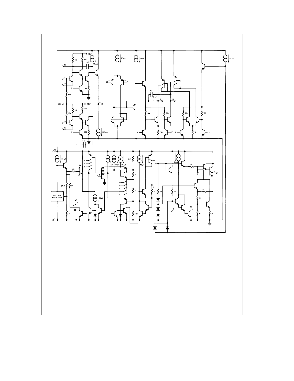
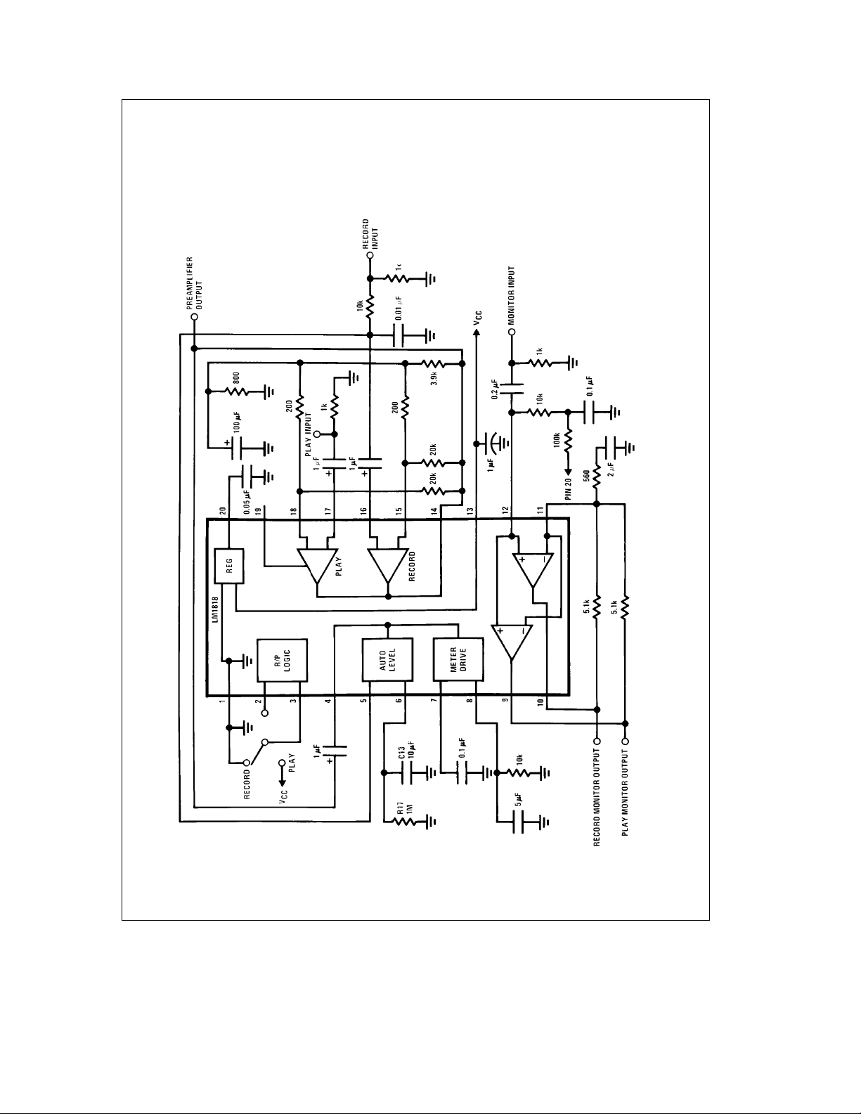
Equivalent Schematic Diagram
FIGURE 4
5
TL/H/7894– 4
Page 6

Typical Performance Characteristics
Automatic Level Control
(ALC) Response Characteristic Preamp Input Noise Voltage Preamp Input Noise Current
Application Hints
PREAMPLIFIERS
There are 2 identical preamplifiers with 1 common output
pin on the IC. One amplifies low level inputs such as a microphone in the record mode and another amplifies the signal from the playback head in the playback mode. The amplifiers use a common capacitor, C6, to set the low frequency pole of the closed loop responses. On the playback amplifier, the collector of the input device is made available so
that an external low noise device can be connected in critical applications. When using an external low noise transistor, pins 17 and 18 of the IC are shorted together to ensure
that the internal input transistor is turned OFF and the external transistor’s collector is tied to pin 19. The input and
feedback connections are now made to the external input
(Figure 5)
TL/H/7894– 5
transistor. The amplifiers are stable for all gains above 5
and have a typical open loop gain of 100 dB. R8 and R9
enable C6 to be quickly charged and set the DC gain. Internal biasing provides a DC voltage independent of temperature at pin 17 so that the preamplifier DC output will remain
relatively constant with temperature. Supply decoupling is
provided by an internal regulator. Additional decoupling can
be added for the input stages by increasing the size of the
capacitor on pin 20 of the IC. A fast charging circuit is connected to the preamplifiers’ input capacitors (pins 16 and
17) to decrease the turn-ON time. Larger input capacitors
decrease the noise by reducing the source impedance at
lower frequencies where 1/f noise current produces an input noise voltage. The input resistance of the preamplifiers
is typically 50 kX.
Quiescent DC Output Voltage
R9
e
a
V
1
DC
(0.5b50c10
R8
#
J
b
6
R2)V if R2aR3l10 R
E
where R
AC Voltage Gain
A
AC
TL/H/7894– 6
FIGURE 5. Preamplifier
6
R8R9
e
E
R8aR9
R3
a
R4
1asC5R3
e
a
R2
1
TL/H/7894– 7
Page 7

Application Hints (Continued)
MONITOR AND RECORD AMPLIFIERS
The monitor and record amplifiers share common input and
feedback connections but have separate outputs. During
playback, the input signal is amplified and appears only at
the playback monitor output. Because the outputs are separate, different feedback components can be used and, as a
result, totally different responses can be set. The amplifiers
are stable for all closed loop gains above 3 and have an
open loop gain of typically 80 dB. The outputs are capable
of supplying a minimum of 400 mA into a load and swing
within 500 mV of either V
is needed to drive a load, an external pull-up resistor on the
or ground. If more than 400 mA
CC
output of these amplifiers can increase the load driving capability.
AUTOMATIC LEVEL CONTROLÐALC
The automatic level control provides a constant output level
for a wide range of record source input levels. The ALC
works on the varying impedance characteristic of a saturat-
(Figure 6)
(Figure 7)
Record gaine1
Playback gain
a
e1a
R15
R14
R16
R14
ed transistor. The impedance of the saturated transistor
forms a voltage divider with the source impedance of a series resistor (R1 in
Figure 9
). The input signal is decreased
as the ALC transistor is increasingly forward biased. The
ALC transistor will be forward biased when the preamplifiers’s AC output (pin 14), coupled to the combination ALCmeter drive input (pin 4) reaches 40 mV peak (25 mVrms).
The gain of the ALC loop is such that a preamp input signal
increase of 10 dB will result ina2dBincrease on the AC
output of the preamplifier. If greater than 25 mVrms is desired at the output of the preamp, a series resistor can be
added between the preamp output coupling capacitor and
the ALC input (pin 4). The input impedance of the ALC circuit is 2 kX; therefore, ifa2kXseries resistor is added,
ALC action will begin at 50 mVrms.
The ALC memory capacitor connected to pin 6 has the additional function of amplifier anti-pop control; for this reason, it
is necessary that a capacitor be connected to pin 6 even if
ALC is not used.
FIGURE 6. Monitor Amplifier
7
TL/H/7894– 8
Page 8

Application Hints (Continued)
FIGURE 7. Auto Level-Meter Circuit
METER DRIVINGÐMOTIONAL PEAK LEVEL
RESPONSE
The meter drive output (pin 8) is capable of supplying 1 –2
mA at a filtered DC voltage that is typically equal to 10 times
the RMS value of the signal applied to the ALC-meter drive
input (pin 4). The RC network connected to pin 7 of the IC
determines the memory constant of the meter circuit. It is
therefore possible to store the peak input signal by giving
this RC network a long time constant, or read the instantaneous signal level by giving this RC network a very short
time constant (i.e., no capacitor). This memory capacitor is
discharged within the integrated circuit at a discharge rate
related to the DC level on the meter output pin. When the
(Figure 7)
TL/H/7894– 9
meter output pin is between 0 V
50 mA discharge current; when the pin is between 0.7V and
1.1V there is no internal discharge current; and when the
voltage on pin 8 is greater than 1.1V there is a discharge
equivalent to a 3.3k resistor across the memory capacitor.
These different discharge rates allow the meter circuit to
display fast, accurate responses on the lower portion of the
meter display, slow responses in the higher portion of the
meter display, and rapid discharge when the voltage is
above the maximum reading the meter can display. The resistor in series with the meter can be adjusted such that the
previously mentioned responses coincide with the proper
points (0 VU and
a
3 VU) on the meter scale.
and 0.7 VDCthere is a
DC
8
Page 9

Application Hints (Continued)
Anti-Pop Circuitry
The capacitor on pin 3 is used in a time delay system in
conjunction with C13, the ALC capacitor, to suppress pops
when switching between record and playback.
trates how this is done. The output amplifier, either record or
playback, is shut off prior to switching and carefully rebiased
after switching takes place. It is therefore required that a
proper ratio is selected between the ALC capacitor and the
logic input RC time constant. The ALC capacitor must be
discharged to 0.7V within the time it takes the logic input
capacitor to: 1) charge from V
ing from record to playback, or 2) discharge from V
0.3 V
when switching from playback to record. These
CC
times would normally be similar; however, the ALC capacitor
can be charged to a different initial value depending upon
the input to the ALC circuit. The maximum value to which
the ALC memory capacitor will normally charge is 3.2V,
therefore, the maximum time allowed for discharging C13 is
given by:
It is now necessary to determine the minimum value for the
R/P logic capacitor. This is done by computing the time
between the 2 voltage switching points using the exponential equations for a single RC network.
(Figure 8)
/2 to 0.7 VCCwhen switch-
CC
(C13cDV)
e
t1
If C13e10 mF, t1e72 ms
e
I
e
C13
1
C13c7.2c10
(3.2V
b
350 mA
4
Figure 8
0.7V)
CC
illus-
/2 to
V
CC
CC
e
0.3 V
Ð
e
(
(72 ms)
0.51
CC
b
(
CC
0.51 R13 C11
e
141 ms
l
t1.
CC
e
t2
R13 C11 In
R13 C11 In
To be sure that C13 is completely discharged, let t2
R13 C11
If C11
R13 should be kept to a value less than 50 kX to insure that
bias current existing from pin 3 does not cause an offset
voltage above 200 mV. Typically this bias current is less
than 3 mA.
Record Playback Switch
When the voltage on pin 3 of the IC is greater than 0.5 V
the internal record-playback switch switches into the playback mode. During playback the record preamplifier remains partially biased but the input signal to this preamp
does not appear at the preamplifier output. In addition, during the playback mode, the record monitor output (pin 9) is
disabled and the ALC circuit operates to minimize the signal
into the record preamp input. The meter circuit is operational in the playback as well as the record mode. Similarly,
during the record mode, the playback preamp input is ignored and the playback monitor output is disabled. In addition, a pin is available to hold one side of the record head at
ground potential while sinking up to 500 mA of AC bias and
record current.
V
0.5 V
Ð
t1
l
0.51
e
10 mF, R13e15 kX
,
FIGURE 8A. Anti-Pop Circuit
9
TL/H/7894– 10
Page 10

Application Hints (Continued)
FIGURE 8B. Waveform for Anti-Pop Circuit
External Components (Refer to
Component External Component Function
R1 Used in conjunction with varying impedance of pin 5, forming a resistor divider 500X –20 kX
C2 Forms a noise reduction system by varying bandwidth as a function of the 0.01 mF –0.5 mF
C1, C3 Coupling capacitors. Because these are part of the source impedance, it is 0.5 mF–10 mF
C4 Radio frequency interference roll-off capacitor 100 pF–300 pF
R2 Playback response equalization. C5 and R3 form a pole in the amplifier 50X –200X
R3 47 kX –3.3 MX
R4 2kX–200 kX
C5
R5 Microphone preamplifier gain equalization 50X –200X
R6 5kX–200 kX
R7 DC feedback path. Provides a low impedance path to the negative input in 0– 2 kX
R8 200X –5 kX
R9 1kX–30 kX
C6 200 mF –1000 mF
C7 0–100 mF
C8 Preamplifier output to monitor amplifier input coupling 0.05 mF–1 mF
C9 ALC coupling capacitor. Note that ALC input impedance is 2 kX 0.1 mF–5 mF
R10 These components bias the monitor amplifier output to half supply since the 10 kX –100 kX
R11 10 kX – 100 kX
R12 10 kX – 100 kX
C10 1 mF –100 mF
network to reduce input level in automatic level control circuit.
changing impedance on pin 5. With a small input signal, the bandwidth is
reduced by R1 and C2. As the input level increases, so does the bandwidth.
important to use the larger values to keep low frequency source impedance at
a minimum.
response at 50 Hz. C5 and R4 form a zero in the response at 1.3 kHz for
120 ms equalization and 2.3 kHz for 70 ms equalization.
order to sink the 50 mA negative input amplifier current. C6, R9, R7 and C7
provide isolation from the output so that adequate gain can be obtained at 20
Hz. This 2-pole technique also provides fast turn-ON settling time.
amplifier is unity gain at DC. This allows for maximum output swing on a
varying supply.
Figure 9
, Monaural Application Circuit)
TL/H/7894– 11
Normal Range
of Value
10
Page 11

External Components (Refer to
Component External Component Function
C11 Exponentially falling or rising signal on pin 3 determines sequencing, time 0–10 mF
R13 0–50kX
R14 R16, R14 and C12 determine monitor amplifier response in the play mode. 1k–100k
R15 30 k X –3 MX
R16 30 k X –3 MX
C12 0.1 mF–20 mF
C13 Determines decay response on ALC characteristic and reduces amplifier pop 5 mF–20mF
R17 100k–
C14 Determines time constant of meter driving circuitry 0.1 mF–10mF
R18 100k–
R19 Meter sensitivity adjust 10 kX –100 kX
C15 Record output DC blocking capacitor 1 mF–10mF
C16 Play output DC blocking capacitor 0.1 mF–10mF
C17 Changes record output response to approximate a constant current output in 500 pF –0.1mF
R21 5kX–100 kX
R22 5kX–100 kX
C18 Preamplifier supply decoupling capacitor. Note that large value capacitor will 0.1 mF – 500 mF
C19 Supply decoupling capacitor 100 mF – 1000 mF
C20 Decouples bias oscillator supply 10 mF – 500mF
R23 Allows bias level adjustment 0–1 kX
R24 Adjusts DC erase current in DC erase machines (for AC erase, see ‘‘Stereo
L1 Optional bias trap 1 mH–30 mH
C21 100 pF–2000 pF
C22 Bias Roll-Off 0.001 mF –0.01 mF
H1 Record/play head 100X –500X;
H2 Erase head (DC type, AC optional) 10X –300X
delay, and operational mode of the record/play anti-pop circuitry. See antipop diagram.
R15, R14 and C12 determine monitor amplifier response in the record mode.
conjunction with record head impedance resulting in proper recording
equalization
increase turn-ON time
Application Circuit,’’
Figure 9
Figure 1
, Monaural Application Circuit) (Continued)
Normal Range
of Value
%
%
)
70 mH–300 mH
11
Page 12

Typical Applications (Continued)
FIGURE 9A. Monaural Application Circuit
12
TOKO America, Inc.
1250 Feehanville Drive
Mount Prospect, IL 60056
TEL: (312) 297-0070
TL/H/7894– 12
Page 13

Typical Applications (Continued)
FIGURE 9B. Level Diagram for Monaural Application Circuit
TL/H/7894– 13
TL/H/7894– 14
13
Page 14

Physical Dimensions inches (millimeters)
Molded Dual-In-Line Package (N)
Order Number LM1818N
NS Package Number N20A
LM1818 Electronically Switched Audio Tape System
LIFE SUPPORT POLICY
NATIONAL’S PRODUCTS ARE NOT AUTHORIZED FOR USE AS CRITICAL COMPONENTS IN LIFE SUPPORT
DEVICES OR SYSTEMS WITHOUT THE EXPRESS WRITTEN APPROVAL OF THE PRESIDENT OF NATIONAL
SEMICONDUCTOR CORPORATION. As used herein:
1. Life support devices or systems are devices or 2. A critical component is any component of a life
systems which, (a) are intended for surgical implant support device or system whose failure to perform can
into the body, or (b) support or sustain life, and whose be reasonably expected to cause the failure of the life
failure to perform, when properly used in accordance support device or system, or to affect its safety or
with instructions for use provided in the labeling, can effectiveness.
be reasonably expected to result in a significant injury
to the user.
National Semiconductor National Semiconductor National Semiconductor National Semiconductor
Corporation Europe Hong Kong Ltd. Japan Ltd.
1111 West Bardin Road Fax: (
Arlington, TX 76017 Email: cnjwge@tevm2.nsc.com Ocean Centre, 5 Canton Rd. Fax: 81-043-299-2408
Tel: 1(800) 272-9959 Deutsch Tel: (
Fax: 1(800) 737-7018 English Tel: (
National does not assume any responsibility for use of any circuitry described, no circuit patent licenses are implied and National reserves the right at any time without notice to change said circuitry and specifications.
Fran3ais Tel: (
Italiano Tel: (
a
49) 0-180-530 85 86 13th Floor, Straight Block, Tel: 81-043-299-2309
a
49) 0-180-530 85 85 Tsimshatsui, Kowloon
a
49) 0-180-532 78 32 Hong Kong
a
49) 0-180-532 93 58 Tel: (852) 2737-1600
a
49) 0-180-534 16 80 Fax: (852) 2736-9960
 Loading...