

Page 1
®
LCP1521
Appl icat ion Sp ecif ic Dis cret es
A.S.D.
FEATURES
Dual programmable transient suppressor
Wide negative firing voltage range:
V
= -150 V max.
MGL
Low dynamic switching voltages: VFP and V
Low gate triggering current: IGT = 2 mA max
Peak pulse current: IPP = 30 A (10/1000 µs)
Holding current: IH = 150 mA
DESCRIPTION
This device has been especially designed to protect new high voltage, as well as classical SLICs,
against transient overvoltages.
Positive overvoltages are clipped with 2 diodes.
Negative surges are suppressed by 2 thyristors, their breakdown voltage being referenced
to -V
This component presents a very low gate triggering current (I
sumption on printed circuit board during the firing
phase.
A particular attention has been given to the internal
wire bonding. The K elvin method c onfiguration ensures reliable protection, reducing the overvoltage
introduced by the parasitic inductances of the wiring L x(dI/dt), especially for very fast transients.
through the gate.
BAT
) in order to reduce the current con-
GT
TM
DGL
PROGRAMMABLE TRANSIENT VOLTAGE
SUPPRESSOR FOR SLIC PROTECTION
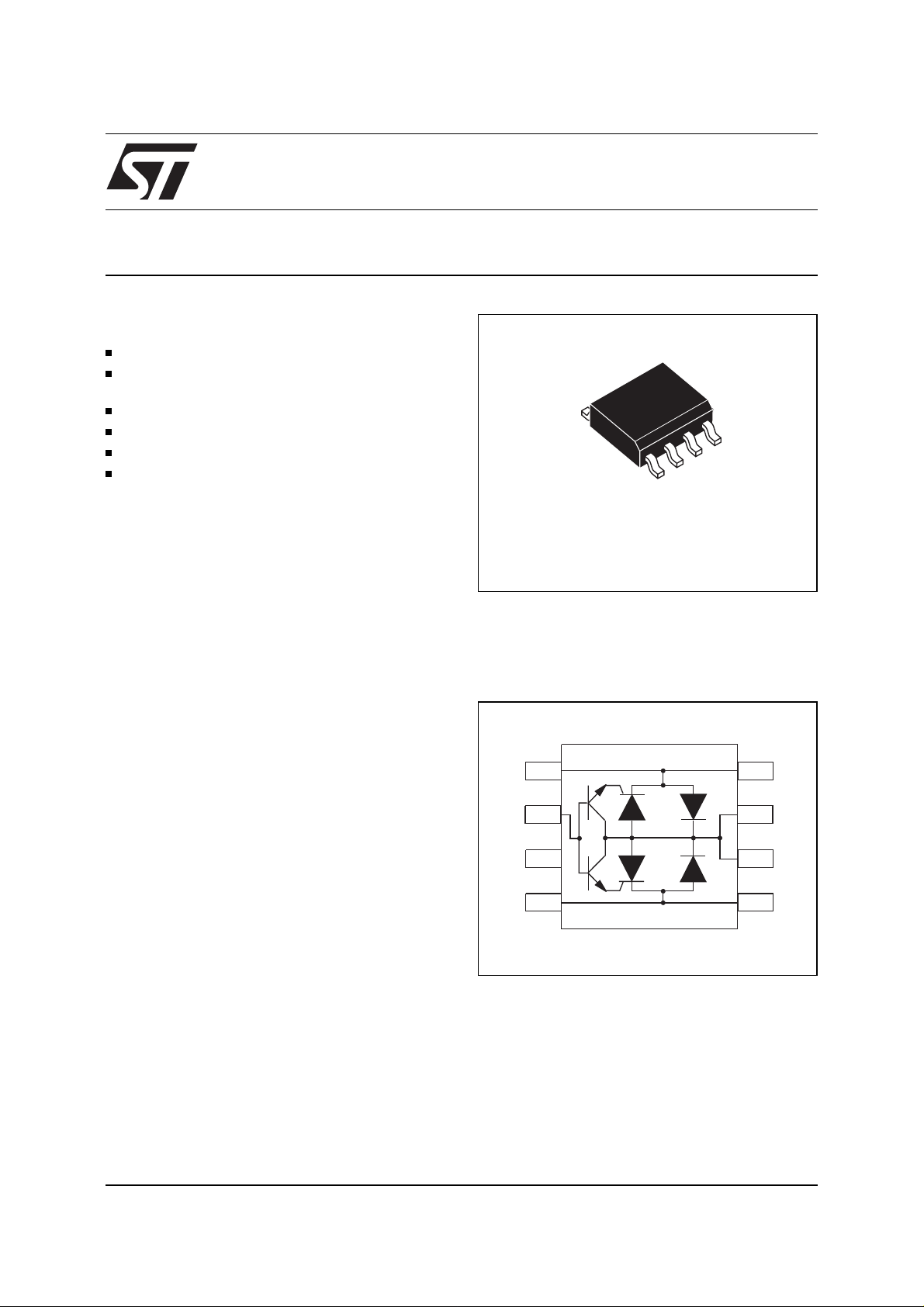
SO-8
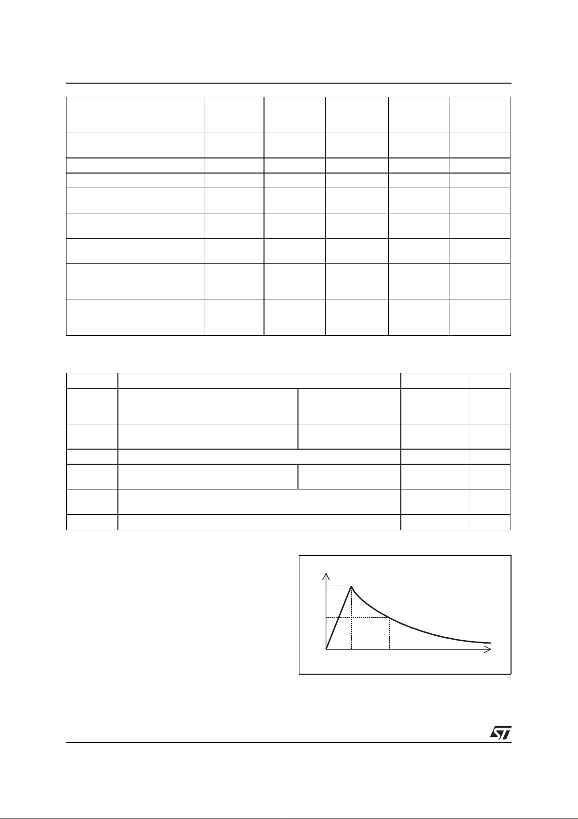
FUNCTIONAL DIAGRAM
TIP
GA TE
NC
RING
TIP
GND
GND
RING
September 1999 - Ed: 2A
1/9
Page 2
LCP1521
COMPLIES WITH THE
FOLLOWING STANDARDS:
ITU-T K20
VDE0433
VDE0878
IEC1000-4-5
FCC Part 68
lightning surge type A
FCC Part 68
Peak Surge
Voltage
(V)
4000
1000
Voltage
Waveform
(µs)
10/700
10/700
Current
Waveform
(µs)
5/310
5/310
Admissible
Ipp
(A)
40
25
2000 10/700 5/310 40 10
2000 1.2/50 1/20 50 2
level 3
level 4
1500
800
10/700
1.2/50
10/160
10/560
5/310
8/20
10/160
10/560
40
100
50
35
1000 9/720 5/320 25 -
Necessary
Resistor
(Ω)
lightning surge type B
BELLCORE:
NWT-001089-CORE
2500
1000
2/10
10/1000
2/10
10/1000
170
30
First level
BELLCORE:
5000 2/10 2/10 170 20
NWT-001089-CORE
Second level
Note 1:
the mentioned value of the series resistance is the minimum value needed to fulfill the standard r equirement.
ABSOL UTE M AXIMU M RA TIN GS
= 25°C, unless otherwise specified).
(T
amb
Symbol Parameter Value Unit
I
PP
I
TSM
I
GSM
V
MLG
V
MGL
T
stg
Tj
T
L
Peak pulse current (see note1)
Non repetitive surge peak on-state curr ent
(F = 50Hz)
Maximum gate current (half sine wave tp = 10ms)
Maximum voltage LINE/GND
Maximum voltage GATE/LINE
Storage temperature range
Maximum junction temperature
Maximum lead temperature for soldering d uring 10s
10/1000µs
5/310µs
2/10µs
tp = 10ms
t = 1s
-40° C < Tamb < +85°C
-40° C < Tamb < +85°C
30
40
170
20
5
2A
-150
-150
- 55 to + 150
150
260
60
10
22
15
10
24
-
-
A
A
V
°
C
°
C
Note 1 :
2/9
Pulse waveform
10 / 1000 µs tr = 10 µs tp = 1000 µs
5 / 310 µstr = 5
2 / 10 µstr = 2
µ
s tp = 310 µs
µ
s tp = 10 µs
100
50
%I
0
PP
t
r
t
p
t
Page 3
LCP1521
THERMAL RESISTANCE
Symbol Parameter Value Unit
Rth (j-a)
Junction to ambient
170
°
C/W
ELECTRICAL CHARACTERISTICS
(T
amb
= 25°C)
Symbol Parameter
I
GT
I
H
I
RM
I
RG
V
RM
V
GT
V
V
FP
V
DGL
V
GATE
V
RG
C
1 - PARAMETERS RELATED TO THE DIODE LINE / GND
Gate triggering current
Holding current
Reverse leakage current LINE / GND
Reverse leakage current GATE / LINE
Reverse voltage LINE / GND
Gate triggering voltage
Forward drop voltage LINE / GND
F
Peak forward voltage LINE / GND
Dynamic switching voltage GATE / LINE
GATE / GND voltage
Reverse voltage GATE / LINE
Capacitance LINE / GND
(T
V
amb
DGL
V
V
R
= 25°C)
RM
V
F
I
RM
I
R
I
H
I
PP
Symbol Test conditions Max Unit
V
F
V
FP
(note 1)
Note 1
: see test circuit for VFP; RP is the protection resistor located on the line card.
Square pulse : tp = 500µs IF = 5A
10/700µs
1.2/50µs
2/10µs
1.5kV
1.5kV
2.5kV
RP = 10Ω
R
= 10Ω
P
R
= 62Ω
P
2V
5
V
7
12
3/9
Page 4

LCP1521
2 - PARAMETERS RELATED TO THE PROTECTION THYRISTOR
(T
amb
= 25°C)
Symbol Test conditions Min Max Unit
V
GND / LINE
V
GATE
at I
Tc=25°C VRG = -150V
Tc=85°C V
V
GATE
V
V
I
I
GT
I
H
GT
RG
DGL
10/700µs
1.2/50µs
2/10µs
Note 2:
see functional holding current (IH) test cir cu i t
Note 3:
see test circuit for V
The oscillations with a time duration lo wer than 50ns are not taken into account
3 - PARAMETERS RELATED TO DIODE AND PROTECTION THYRISTOR
= -48V
= -48V (see note 2)
GT
= -150V
RG
= -48V (see note 3)
1kV
1.5kV
2.5kV
DGL
R
R
R
= 10Ω
P
= 10Ω
P
= 62Ω
P
I
PP
I
PP
I
PP
= 30A
= 30A
= 38A
0.1 2 mA
150 mA
1.5 V
5
50
7
10
25
(T
= 25°C)
amb
Symbol Test conditions Max Unit
I
RM
Tc=25°C V
Tc=85°C V
GATE / LINE
GATE / LINE
= -1V VRM = -150V
= -1V VRM = -150V
5
50
µ
A
V
µ
A
C
VR = -3V F = 1MHz
= -48V F = 1MHz
V
R
100
50
pF
4/9
Page 5

FUNCTIONAL HOLDING CURRENT (IH) TEST CIRCUIT : GO-NO GO TEST
R
LCP1521
-V
P
V
BAT
=
- 100V
D.U.T.
This is a GO-NO GO test which allows to confirm the holding current (I
TEST PROCEDURE :
- Adjust the current level at the I
- Fire the D.U.T. with a surge current : I
value by short circuiting the D.U.T.
H
= 10A, 10/1000µs.
PP
- The D.U.T. will come back to the off-state within a duration of 50ms max.
TEST CIRCUIT FOR VFP AND V
(V is defined in unload condition )
P
PARAMETERS
DGL
L
R
2
Surge generator
) level in a functional test circ uit.
H
R
4
TIP
RING
R
3
V
CC
P
1
R
1
2
GND
Pulse (µs) V
t
r
t
p
p
(V) (µF) (nF) (µH) (Ω)(
10 700 1500 20 200 0 50 15 25 25 30 10
1.2 50 1500 1 33 0 76 13 25 25 30 10
2 10 2500 10 0 1.1 1.3 0 3 3 38 62
C
1
C
2
LR
1
R
2
Ω
)(
R
3
Ω
)(
R
4
Ω
IPPR
)(A)(
Ω
p
)
5/9
Page 6

LCP1521
TECHNICAL INFORMATION
Fig. A1:
LCP1521 concept behavior.
L 1
GND
L 2
-Vbat
Rs1
Rs2
TIP
IG
Gate
C
T1
Th1
RING
ID1
D1
VTip
GND
V Ring
Figur e A1 shows the class ic al pr otecti on c irc uit us ing th e L CP152 1 crowb ar c onc ept. This to polog y
has been developed to protect the new high voltage SLIC’s, it allows to program the negative firing
threshold whil e the positive clamping va lue is fixed at GND.
When a negative surge occurs on one wire (L1 for example) a current Ign flows through the base of the
transistor T1 and then injects a current in the gate of the thyristor Th1. Th1 fires and all the surge current
flows through the ground. After the surge when the current flowing through Th1 becomes less negative
than the holding current I
, then Th1 switches off.
H
When a positive surge occurs on one wire (L1 for example) the diode D1 conducts and the surge current
flows through the ground.
Fig. A2:
Example of PCB layout based on LCP1521 protection.
To the
line side
nF
0
GND
To the
SLIC side
22
In order to minimize the remaining voltage across the S LIC inputs during the surge, the TIP and RING pins
of the LCP1521 are doubled (Pins 1 and 8 for TIP / Pins 4 and 5 for RING).
This fact allows the board designer to connect the track like designed in figure A2. With such a PCB design,
the extra voltages caused by track stray inductance (LdI / dt) remain located on the line side of the LCP and
do not affects its SLIC side.
The capacitor C is used to speed up the crowbar structure firing during the fast surge edges.
This allows to minimize the dynamical breakover voltage at the SLIC Tip and Ring inputs during fast strikes.
Please note that this capacitor is generally present around the SLIC - Vbat pin.
So to be efficient it has be as close as possible from the LCP1521 Gate pin and from the reference ground
track (or plan) (see Fig. A2). The optimized value for C is 220nF.
6/9
Page 7

LCP1521
The series resitors Rs1 and Rs2 designed in figure 1 represent the fuse resistors or the PTC which are mandatory to withstand the power contact or the power inductance tests imposed by the different country standards. Ta ki ng i nt o ac co unt thi s f ac t t he a ctu al li ghtni n g s urg e c urre n t fl owi ng t hro ug h th e L CP is eq ua l to :
I surge = V surge / (Rg + Rs)
With V surge = peak surge voltage imposed by the standard.
Rg = series resistor of the surge generator
Rs = series resistor of the line card (e.g. PTC)
e.g. For a line card with 30Ω of series resistors which has to be qualified under Bellcore 1000V 10/1000µs
surge, the actual current through the LCP1521 is equal to:
I surge = 1000 / (10 + 30) =
25A
The LCP1521 is particularly optimized for the new telecom applications such as the fiber in the loop, the
WLL, the decentralized central office for example. These short line applications need smaller operating
voltages than the long line applications and then allow the use of high voltage SLIC’s operating without ring
relay. The schematics of figure A3 gives the most frequent topology used for these emergent applications.
Fig. A3:
Protection of high voltage SLIC.
GND
Line
Rs (*)
Rs (*)
220nF
Gate
GND
TIP
RING
-Vbat
TIP
GND
SLIC
RING
LCP1521
Line card
Rs (*) = PTC or Res ito r fu se
7/9
Page 8

LCP1521
Surge peak current versus overload duration.
ITSM (A)
20
18
16
14
12
10
8
6
4
2
0
0.01 0.1 1 10 100 1000
t(s)
ORDER CODE
LCP 1 5 2 1 RL
Relative variation of holding current versus junction temperature
IH [Tj] / IH [Tj=25°C ]
1.8
1.6
1.4
1.2
1.0
0.8
0.6
0.4
0.2
0.0
-40 -20 0 20 40 60 80 100
Tj(°C)
LINE CARD
PRO TECTION
I = 150 mA
H
VERSION
PACKAGE
1 : SO-8
RL :Tape & Reel
:Tube
8/9
Page 9

PACKAGE ME CHANICAL D AT A
SO-8 (Plas tic )
L
A
a2
b
8
1
e
e3
D
M
5
4
S
F
LCP1521
DIMENSIONS
REF.
c1
C
a3
b
a
1
E
1
A 1.75 0.069
a1 0.1 0.25 0.004 0.010
a2 1.65 0.065
a3 0.65 0.85 0.025 0.033
b 0.35 0.48 0.014 0.019
b1 0.19 0.25 0.007 0.010
C 0.25 0.50 0.50 0.010 0.020
c1 45° (typ )
D 4.8 5.0 0.189 0.197
E 5.8 6.2 0.228 0.244
e 1.27 0.050
e3 3.81 0.150
F 3.8 4.0 0.15 0.157
L 0.4 1.27 0.016 0.050
M 0.6 0.024
S8
Millimetre s Inche s
Min. Typ. Max. Min. Typ. Max.
°
(max)
Order code Marking Package Weight Base qty Delivery mode
LCP1521 151DH V SO-8 0.08 g 2500 Tube
LCP1521RL 151DHV SO-8 0.08 g 2000 Tape & Reel
Information furnished is believed to be accurate and reliable. However, STMicroelectronics assumes no responsibility for the consequences of
use of such information nor for any infringement of patents or other rights of third parties which may result from its use. No license is granted
by implication or otherwise under any patent or patent rights of STMicroelectronics. Specifications mentioned in this publication are subject to
change without notice. This publication supersedes and replaces all information previously supplied.
STMicroelectronics products are not authorized for use as critical components in life support devices or systems without express writte n a pproval of STMicroelectronics.
The ST logo is a registered trademark of STMicro electroni cs
© 1999 STMicroelectronics - Printed in Italy - All rights reserved.
STMicroelectronics GROUP OF COMPANIES
Australia - Brazil - China - Finland - France - Germany - Hong Kong - India - Italy - Japan - Malaysia
Malta - Morocco - Singapore - Spain - Sweden - Switzerland - United Kingdom - U.S.A.
http://www.st.com
9/9
 Loading...