

Page 1
®
LCP02-150B1
A.S.D.™
FEATURES
Protection IC recommended for ringing SLICs.
■
Wide firing voltage range: from -110V to +95V.
■
Low gate triggering current: IG= 5mA max.
■
Peak pulse current: IPP= 30A (10/1000µs) .
■
Holding current: IH= 150mA min.
■
UL497B approved (file E136224)
■
MAIN APPLICATIONS
Dual battery supply voltage SLICs
■
- negative battery supply configuration
-negative & positivebattery supply configuration
■ Central Office (CO)
■ Private Branch Exchange (PBX)
Digital Loop Carrier (DLC)
■
■ AsymmetricalDigital Subscriber Line(ADSL G.Lite)
■ Fiber in the Loop (FITL)
■ Wireless Local Loop (WLL)
■
Hybrid Fiber Coax (HFC)
■
ISDN Terminal Adapter
■
Cable modem
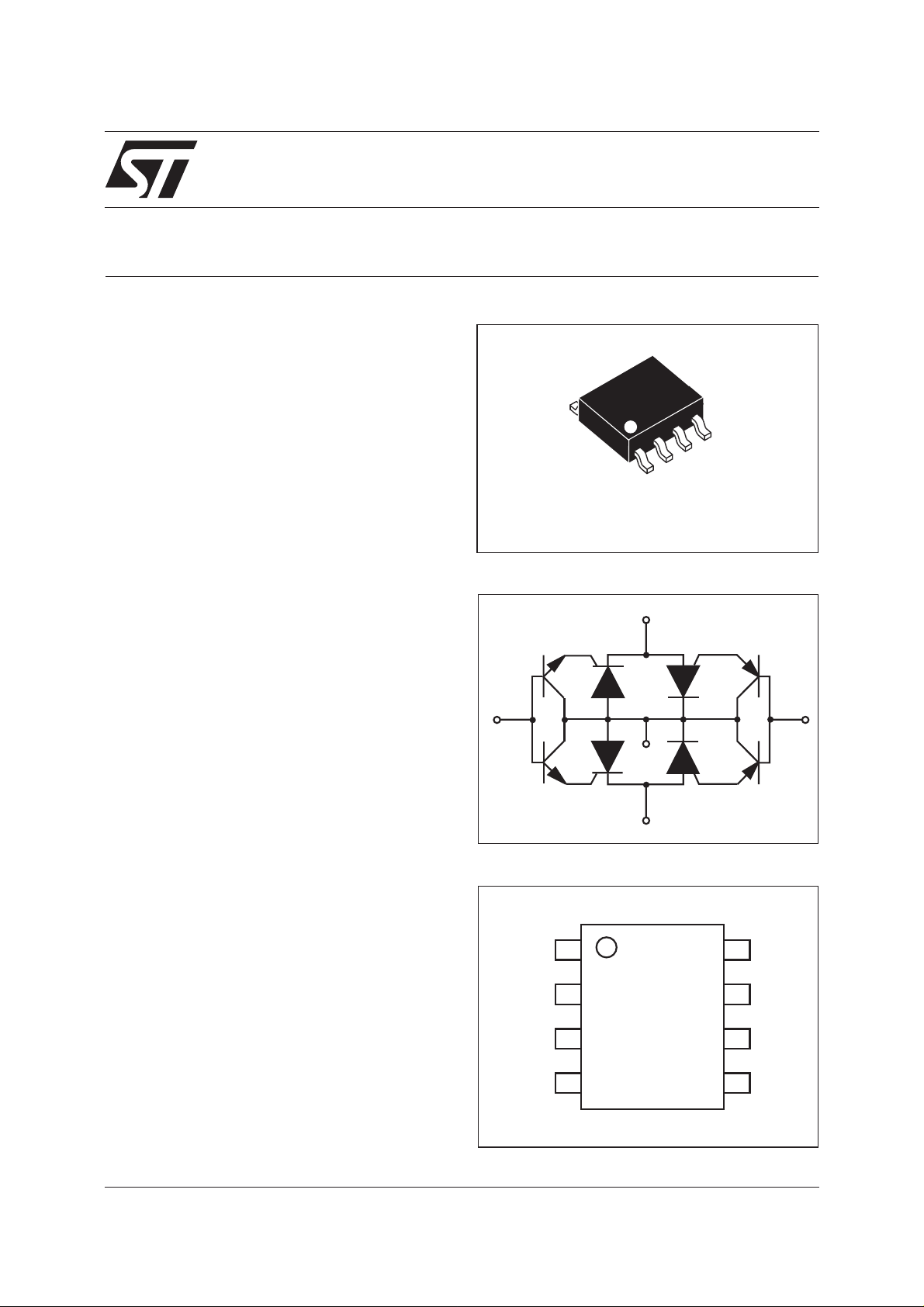
PROTECTION IC
FOR RINGING SLICS
SO-8 WIDE
FUNCTIONAL DIAGRAM
TIP
Gn
GND
Gp
DESCRIPTION
The LCP02-150B1 has been developed to protect
SLICsoperatingonboth negativeand positivebattery supplies, as well as on high voltage SLICs. It
providescrowbar modeprotection for bothTIP and
RINGlines. Thesurge suppression isassumed for
each wire by two thyristor structures, one dedicated to positive surges the second one for negative surges. Both positive and negative threshold
levels are programmable by two gates (Gn and
Gp). The use of transistors decreases the battery
currents during surge suppression.
The LCP02-150B1 has high Bellcore Core, ITU-T
and FCC Part 68 lightning surge ratings, ensuring
rugged performance in the field. In addition, it is
also specified to assist a designer to comply with
UL1950, IEC950 and CSA C22.2. It is UL 497B
approved (file E136224), and has UL94-V0resin
approved
TM: ASD is trademarks of STMicroelectronics.
September 2000 - Ed: 4A
RING
PIN-OUT CONFIGURATION
TIP
G
n
G
P
RING
NC
GND
GND
NC
1/8
Page 2
LCP02-150B1
COMPLIES WITH FOLLOWING STANDARDS
ITU-T K20
ITU-T K21
VDE0433
VDE0878
IEC61000-4-5
FCC Part 68
lightning surge type A
FCC Part 68
lightning surge type B
BELLCORE
GR-1089-CORE
First level
BELLCORE
GR-1089-CORE
Second level
BELLCORE
GR-1089-CORE
Intrabuilding
Peak surge
voltage
(V)
4000
1000
4000
1500
Voltage
waveform
(µs)
10/700
10/700
10/700
10/700
Required
peak current
(A)
100
25
100
37.5
Current
waveform
(µs)
5/310
5/310
5/310
5/310
Minimum serial
resistor to meet
2000 10/700 50 5/310 5
2000 1.2/50 50 1/20 0
level 3
level 4
1500
800
10/700
1.2/50
10/160
10/560
50
100
200
100
5/310
8/20
10/160
10/560
1000 9/720 25 5/320 0
2500
1000
2/10
10/1000
500
100
2/10
10/1000
5000 2/10 500 2/10 40
800
1500
2/10
2/10
100
100
2/10
2/10
standard (
50
0
50
0
5
25
20
15
20
25
0
0
)
ABSOLUTE MAXIMUM RATINGS (T
amb
=25°C)
Symbol Parameter Value Unit
I
I
TSM
PP
Peak pulse current
Non repetitive surge peak on-state current
(F = 50Hz)
V
max
GN
max
V
GP
∆ V
bat
T
op
T
stg
T
L
Note 1: Within the Top range, the LCP02-150B1 keeps on operating.
The impacts of the ambient temperature are given by derating
curves.
Maximum negative battery voltage range
Maximum positive battery voltage range
Total battery supply voltage
max
Operating temperature range (see note 1)
Storage temperature range
Lead solder temperature (10s duration)
10/1000µs
5/310µs
1/20µs
= 0.2 s
t
p
=1s
t
p
=15min
t
p
30
45
65
5.5
4.2
1.5
See fig.1 -110to 0
0to+95
190
-20 to +85 °C
-55to+150 °C
260 °C
%I
PP
100
50
0
t
t
p
r
t
A
A
V
2/8
Page 3
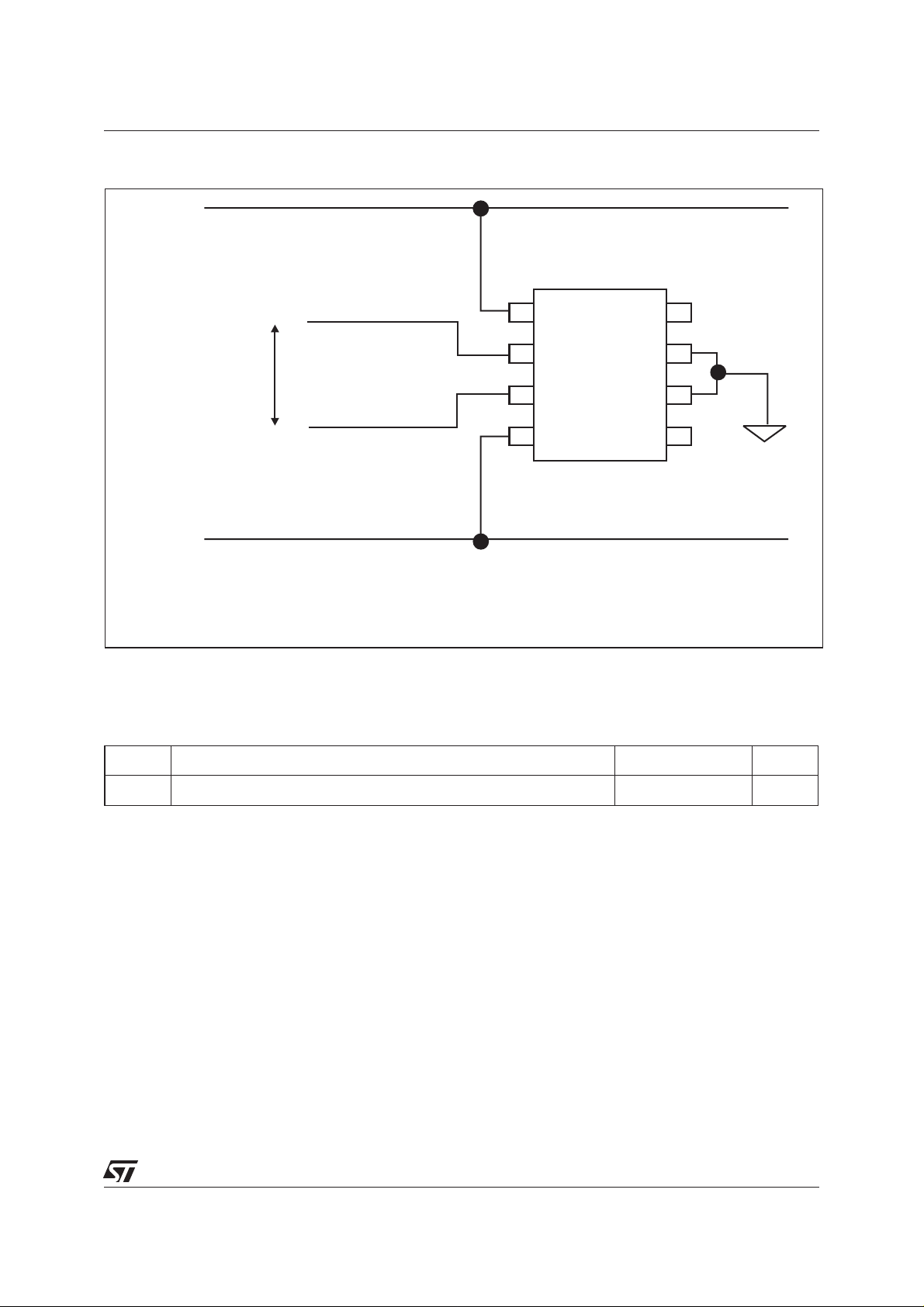
Fig. 1: Test circuit
TIP
LCP02-150B1
Gn from -110V to +0V
∆≤Vbat 190V
RING
Gn connected to negative supply voltage
Gp connected to positive supply voltage
ba GpGn
V t: differential voltage betweenV and V∆
THERMAL RESISTANCE
Gp from +0V to +95V
1
TIP
n
G
P
G
RING
NC
GND
GND
NC
Symbol Parameter Value Unit
R
th (j-a)
Junction to ambient
150 °C/W
3/8
Page 4

LCP02-150B1
ELECTRICAL CHARACTERISTICS (T
amb
= 25°C)
1 - PARAMETERS RELATED TO THE NEGATIVE SUPPRESSOR
Symbol Parameter Test conditions Min. Max. Unit
I
Gn
I
H-
Negative gate trigger
current
Holding current
V
Gn/GND
= -60V
Measured at 50Hz
Go-No Go test, VGn= -60V 150
5mA
(see fig.2)
I
RGL-
Reverse leakage
Tj = 25°C, V
Gn/line
= -190V
5µA
current Gn/Line
V
DGL-
Dynamic switching
voltage Gn / Line
(see note 2)
V
Gn/GND
= -60V
10/1000µs 1kV R
10/700µs 2kV R
1.2/50µs 2kV R
=25ΩIPP= 30A
P
=25ΩIPP= 30A
P
=25ΩIPP= 30A
P
18
8
15
2 - PARAMETERS RELATED TO THE POSITIVE SUPPRESSOR
Symbol Parameter Test conditions Min. Max. Unit
I
Gp
I
RGL+
Positive gate trigger
current
Reverse leakage
V
Gp/GND
= 60V
Measured at 50Hz
Tj = 25°C, V
Gp/line
= +190V
5mA
5µA
current Gp/LINE
mA
V
V
DGL+
Dynamic switching
voltage Gp / Line
(see note 2)
V
Gp/GND
= +60V
10/1000µs 1kV R
10/700µs 2kV R
1.2/50µs 2kV R
=25ΩIPP= 30A
P
=25ΩIPP= 30A
P
=25ΩIPP= 30A
P
18
8
35
3 - PARAMETERS RELATED TO LINE/GND
Symbol Parameter Test conditions Typ. Max. Unit
I
R
Reverse
leakage current
C
off
Capacitance
Tj = 25°C, V
Tj = 25°C, V
= +90V, V
LINE
= -105V, V
LINE
GP/LINE
GN/LINE
= +1V
= -1V
VR= -3V, F =1MHz, VGp= 60V, VGn= -60V
5
5
60 pF
LINE/GND
Note 2: The V
value is the difference between the peak line voltage during the surge and the programmed gate voltage.
DGL
V
µA
4/8
Page 5

LCP02-150B1
Fig. 2: Relative variation of holding current versus
junction temperature.
IH (T) / IH(25°C)
1.6
1.4
1.2
1
0.8
0.6
0.4
-20 0 20 40 60 80 100
T (°C)
Fig. 4: Capacitance versus reverse applied
voltage (typical values) with V
= +90V.
V
GP
= -90V and
GN
Fig. 3: Maximum non repetitive surge peak on
state current versus overload duration (with 50Hz
sinusoidal wave and initial junction temperature
equal to +25°C).
I (A)
TSM
10
8
6
4
2
0
0.01 0.1 1 10 100 1000
t (s)
70
60
50
40
30
20
10
0
C (pF)
line +
line -
Vline (V)
20 40 60 80 100
5/8
Page 6

LCP02-150B1
TECHNICAL INFORMATION
Fig. 5: LCP02 concept behavior.
Rs1
L 1
GND
-Vbat
TIP
VTip
Ign Igp
Gn
T1
Th1
Th2
T2
Gp
+Vb
Cp
Rs2
Cn
RING
GND
L 2
V Ring
Figure 5 shows the classical protection circuit using the LCP02 crowbar concept. This topology has been
developped to protect the new two-battery voltage SLICs. Itallows both positive and negative firing thresholds
to be programmed. The LCP02-150B1 has two gates (Gn and Gp). Gn is biasedto negative battery voltage
-Vbat, while Gp is biased to the positive battery voltage +Vb.
When a negative surge occurs on one wire (L1 for example), a current Ign flows through the base of the
transistor T1 and then injects a current in the gate of the thyristor Th1 which fires. All the surge current
flows through the ground. After the surge, when the current flowing through Th1 becomes less negative
than the negative holding current Ih-, Th1 switches off. This holding current I
as per figure2.
When a positive surge occurs on one wire (L1 for example), a current Igp flows through the base of the
transistor T2 and then injects a current in the gate of the thyristor Th2 which fires. All the surge current
flows through the ground. After the surge, when the current flowing through Th2 becomes less positive
than the positive holding current Ih+, Th2 switches off. This holding current I
temperature dependant and the same figure 2 also applies.
The capacitors Cn and Cp are used to speed up the crowbar structure firing during the fast rise or fall
edges.This allows tominimize thedynamicalbreakover voltageat the SLICTip and Ringinputs during fast
surges. Please note that these capacitors are generally available around the SLIC. To be efficient they
have to be as close as possible to the LCP02-150B1 gate pins (Gn and Gp) and to the reference ground
track (or plan). The optimized value for Cn and Cp is 220nF.
The series resistors Rs1 and Rs2 designed in figure 5 represent the fuse resistors or the PTCs which are
needed to withstand the power contact or the power induction tests imposed by the country standards.
Taking this factor into account, the actual lightning surge current flowing through the LCP02-150B1 is
equal to :
I surge = Vsurge / (Rg + Rs)
is temperature dependant
H-
, typically 20mA at 25°C, is
H+
With V surge = peak surge voltage imposed by the standard.
Rg = series resistor of the surge generator
Rs = series resistor of the line card (e.g. PTC)
e.g.:
Fora line cardwith 50Ωof series resistorswhich hasto be qualifiedunder Bellcore 1000V10/1000µs
surge, the present current through the LCP02-150B1 is equal to :
I surge = 1000 / (10 + 50) = 17A
6/8
Page 7

LCP02-150B1
The LCP02-150B1 topology is particularly optimized for the new telecom applications such as fiber in the
loop, WLL systems, decentralized central office for example. The schematics of figures 6 and 7 give the 2
most frequent topologies used for these emergent applications
Fig. 6: Protection of SLIC with positive and negative battery voltages.
Line card
-Vbat
Rs (*)
TIP
Line
GND
Rs (*)
Rs (*) = PTC or Resistor fuse
Fig. 7: Protection of high voltage SLIC
Line card
Rs (*)
GND
220nF
Line
Rs (*)
220nF
Gn
Gn
LCP02
TIP
LCP02
RING
TIP
RING
Gp
Gp
220nF
SLIC
RING
+Vb
-Vbat
TIP
SLIC
RING
Rs (*) = PTC or Resistor fuse
Figure 6 shows the classical protection topology for SLIC using both positive and negative battery voltages. With such a protection the SLIC is protected against surge over +Vb and lower than -Vbat. In this
case, +Vb can be programmed up to +95V while -Vbat can be programmed down to -110V. Please note
that the differential voltage does not exceed ∆V
max at 190V.
bat
Figure 7 gives the protection topology for the new SLIC using high negative voltage down to -110V.
7/8
Page 8

LCP02-150B1
PACKAGE MECHANICAL DATA
SO-8 Wide Plastic
D
b
e
8
1
ORDER CODE
REF.
DIMENSIONS
Millimetres Inches
L
Min. Typ. Max. Min. Typ. Max.
A 2.50 0.099
A2
A
K
A1
E
C
A1 0.25 0.010
A2 1.51 2.00 0.059 0.079
b 0.35 0.40 0.51 0.013 0.016 0.020
c 0.10 0.20 0.35 0.003 0.008 0.014
5
E1
D 6.05 0.239
E 5.02 6.22 0.197 0.245
E1 7.62 8.89 0.30 0.35
4
e 1.27 0.05
K 10°
L 0.50 0.80 0.019 0.032
Ordering Type Marking Package Weight Base qty Delivery mode
LCP02-150B1 LCP02 SO-8-Wide 0.13g 90 Tube
LCP02-150B1RL 1500 Tape& Reel
Informationfurnished is believed to be accurateand reliable. However, STMicroelectronics assumes noresponsibility for the consequences of
useof such information nor for any infringement of patents or other rights of third partieswhich may result from its use. No licenseis granted by
implication or otherwise under any patent or patent rights of STMicroelectronics. Specifications mentioned in this publication are subject to
change without notice. This publication supersedes and replaces all information previously supplied.
STMicroelectronics products are not authorized for use as critical components in life support devices or systems without express written approval of STMicroelectronics.
The ST logo is a registered trademark of STMicroelectronics
© 2000 STMicroelectronics - Printed in Italy - All rights reserved.
STMicroelectronics GROUP OF COMPANIES
Australia - Brazil - China - Finland - France - Germany - Hong Kong - India - Italy - Japan - Malaysia
Malta - Morocco - Singapore - Spain - Sweden - Switzerland - United Kingdom - U.S.A.
http://www.st.com
8/8
 Loading...