

Page 1

DISCRETE SEMICONDUCTORS
DATA SH EET
LBE2003S; LBE2009S
NPN microwave power transistors
Product specification
Supersedes data of 1997 Mar 03
1998 Feb 16
Page 2
Philips Semiconductors Product specification
NPN microwave power transistors LBE2003S; LBE2009S
FEATURES
• Diffused emitter ballasting resistors
• Self-aligned process entirely ion implanted and gold
metallization
• Optimum temperature profile
• Excellent performance and reliability.
APPLICATIONS
• Common emitter class-A linear power amplifiers up
to 4 GHz.
DESCRIPTION
The LBE2003S and LBE2009S are NPN silicon planar
epitaxial microwave power transistors in a SOT441A metal
ceramic studless package.
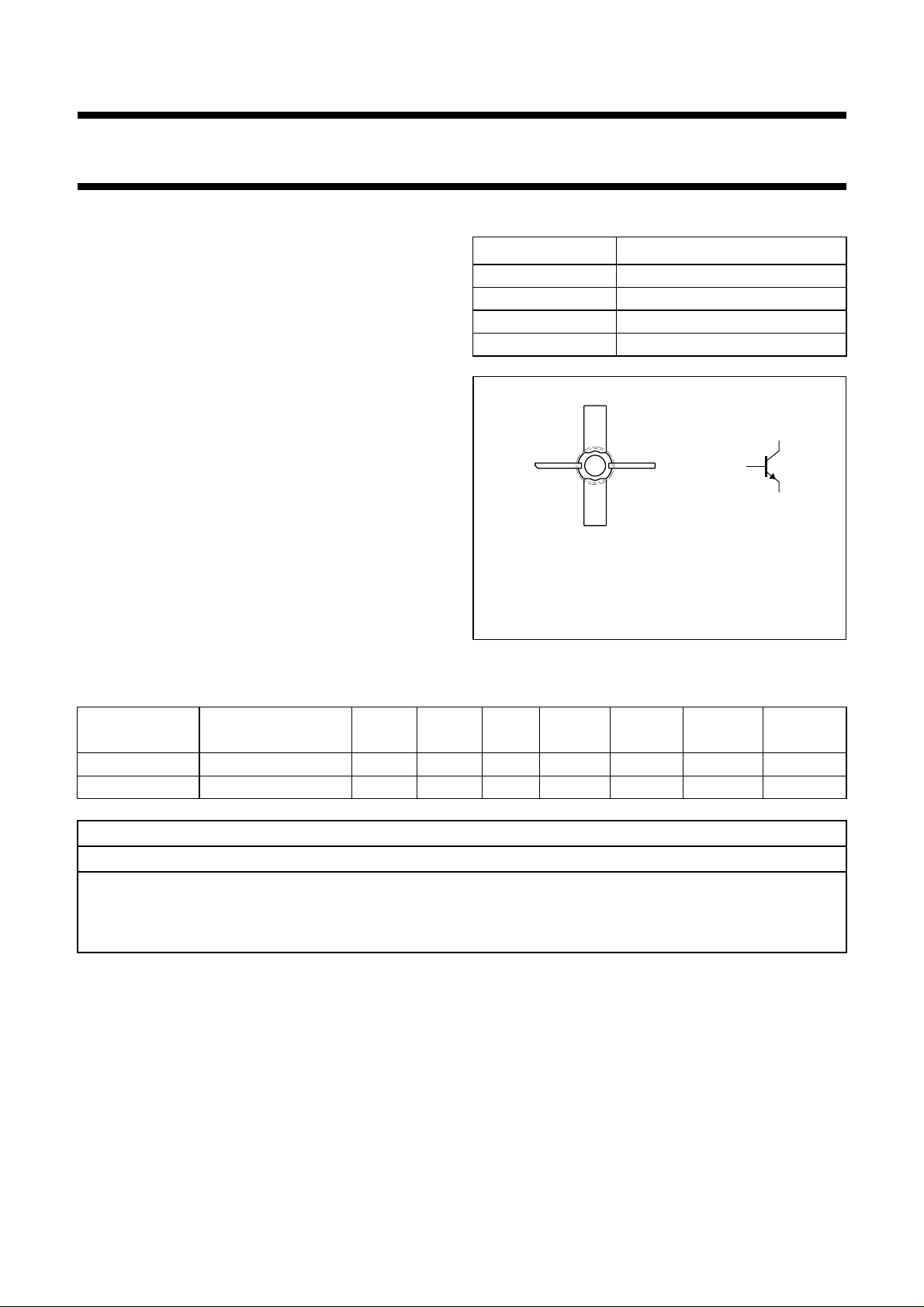
PINNING
PIN DESCRIPTION
1 collector
2 emitter
3 base
4 emitter
handbook, halfpage
Marking code: LBE2003S = 407; LBE2009S = 409.
1
Top view
4
3
b
2
Fig.1 Simplified outline and symbol (SOT441A).
c
e
MAM329
QUICK REFERENCE DATA
Microwave performance up to T
TYPE NUMBER
MODE OF
OPERATION
=25°C in a common emitter class-A amplifier.
mb
f
(GHz)
V
(V)
CE
I
C
(mA)
P
L1
(mW)
G
po
(dB)
Z
(Ω)
i
Z
L
(Ω)
LBE2003S Class-A (CW) linear 2 18 30 ≥200 ≥10 6.2 + j30 17.5 + j7
LBE2009S Class-A (CW) linear 2 18 110 ≥700 ≥9 7.5 + j15 17.5 + j39
WARNING
Product and environmental safety - toxic materials
This product contains beryllium oxide. The product is entirely safe provided that the BeO disc is not damaged.
All persons who handle, use or dispose of this product should be aware of its nature and of the necessary safety
precautions. After use, dispose of as chemical or special waste according to the regulations applying at the location of
the user. It must never be thrown out with the general or domestic waste.
1998 Feb 16 2
Page 3
Philips Semiconductors Product specification
NPN microwave power transistors LBE2003S; LBE2009S
LIMITING VALUES
In accordance with the Absolute Maximum Rating System (IEC 134).
SYMBOL PARAMETER CONDITIONS MIN. MAX. UNIT
V
CBO
V
CER
V
CEO
V
EBO
I
C
P
tot
T
stg
T
j
T
sld
collector-base voltage open emitter 40 V
collector-emitter voltage
LBE2003S R
LBE2009S R
= 220 Ω−35 V
BE
= 100 Ω−35 V
BE
collector-emitter voltage open base − 16 V
emitter-base voltage open collector − 3V
collector current (DC)
LBE2003S − 90 mA
LBE2009S − 250 mA
total power dissipation Tmb≤ 75 °C
LBE2003S − 1.4 W
LBE2009S − 3.5 W
storage temperature −65 +150 °C
operating junction temperature − 200 °C
soldering temperature at 0.3 mm from case; t = 10 s − 235 °C
2
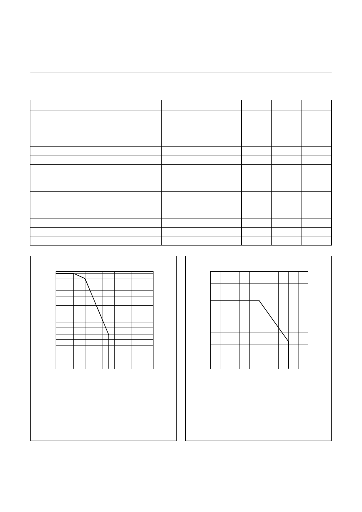
10
handbook, halfpage
I
C
(mA)
(2)
(1)
10
1
10
15 20
Tmb≤ 75°C.
(1) Region of permissible DC operation.
(2) Permissible extension provided RBE≤ 220 Ω.
(3) Second breakdown limit (independent of temperature).
(3)
40 60 100
30
Fig.2 DC SOAR; LBE2003S.
MGD996
VCE (V)
handbook, halfpage
2
P
tot
(W)
1.5
1
0.5
0
−50 0 200
50 100 150
MGD989
Tmb (oC)
Fig.3 Power dissipation derating as a function of
mounting-base temperature; LBE2003S.
1998 Feb 16 3
Page 4
Philips Semiconductors Product specification
NPN microwave power transistors LBE2003S; LBE2009S
3
10
handbook, halfpage
I
C
(mA)
2
10
(1)
10
1
10 20 40
Tmb≤ 75 °C.
(1) Region of permissible DC operation.
(2) Permissible extension provided RBE≤ 100 Ω.
(3) Second breakdown limit (independant of temperature).
(3)
(2)
VCE (V)
Fig.4 DC SOAR; LBE2009S.
MGD990
handbook, halfpage
2
10
4
P
tot
(W)
3
2
1
0
−50 0
50 100 150
MGD991
Tmb (
200
o
C)
Fig.5 Power dissipation derating as a function of
mounting-base temperature; LBE2009S.
THERMAL CHARACTERISTICS
SYMBOL PARAMETER CONDITIONS MAX. UNIT
R
th j-mb
thermal resistance from junction to mounting-base Tj=75°C
LBE2003S 65 K/W
LBE2009S 36 K/W
R
th mb-h
thermal resistance from mounting-base to heatsink Tj=75°C 1.5 K/W
1998 Feb 16 4
Page 5

Philips Semiconductors Product specification
NPN microwave power transistors LBE2003S; LBE2009S
CHARACTERISTICS
T
=25°C unless otherwise specified.
mb
SYMBOL PARAMETER CONDITIONS MIN. TYP. MAX. UNIT
I
CBO
I
CBO
I
CER
I
EBO
h
C
C
C
FE
cb
ce
eb
collector cut-off current VCB= 20 V; IE=0 −−0.1 µA
collector cut-off current VCB= 40 V; IE=0
LBE2003S −−150 µA
LBE2009S −−250 µA
collector cut-off current
LBE2003S V
LBE2009S V
= 35 V; RBE= 220 Ω− − 500 µA
CB
= 35 V; RBE= 100 Ω− − 1000 µA
CB
emitter cut-off current VEB= 1.5 V; IC=0
LBE2003S −−0.05 µA
LBE2009S −−0.2 µA
DC current gain VCE=5V; IC=30mA 15 − 150
V
=5V; IC= 110 mA 15 − 150
CE
collector-base capacitance VCB= 18 V; VEB= 1.5 V;
IE=IC= 0; f = 1 MHz
LBE2003S − 0.3 − pF
LBE2009S − 0.6 − pF
collector-emitter capacitance VCE= 18 V; VEB= 1.5 V;
IE=IC= 0; f = 1 MHz
LBE2003S − 0.45 − pF
LBE2009S − 0.6 − pF
emitter-base capacitance VCB= 10 V; VEB=1V;
IE=IC= 0; f = 1 MHz
LBE2003S − 1.7 − pF
LBE2009S − 3.3 − pF
1998 Feb 16 5
Page 6

Philips Semiconductors Product specification
NPN microwave power transistors LBE2003S; LBE2009S
Table 1 Scattering parameters LBE2003S: VCE= 18 V; IC= 30 mA (VCE and IC regulated); Tmb=25°C; Zo=50Ω;
typical values. (The figures given between brackets are values in dB).
f
(MHz)
S
MAGNITUDE
(ratio)
11
ANGLE
(deg)
S
MAGNITUDE
(ratio)
21
ANGLE
(deg)
MAGNITUDE
(ratio)
S
12
ANGLE
MAGNITUDE
(deg)
(ratio)
S
22
ANGLE
(deg)
500 0.56 −143 0.037 (−28.6) 41 9.50 (19.6) 101 0.56 −34
600 0.55 −154 0.040 (−28.0) 39 8.28 (18.4) 93 0.51 −35
700 0.55 −164 0.040 (−27.9) 40 7.13 (17.1) 88 0.50 −36
800 0.55 −171 0.041 (−27.7) 40 6.35 (16.1) 82 0.49 −37
900 0.55 −178 0.043 (−27.4) 41 5.69 (15.1 77 0.47 −38
1000 0.55 176 0.045 (−26.9) 40 5.14 (14.2 72 0.46 −39
1100 0.55 170 0.048 (−26.4) 40 4.72 (13.5 68 0.46 −39
1200 0.55 165 0.051 (−25.9) 41 4.37 (12.8 64 0.45 −41
1300 0.56 159 0.056 (−25.1) 41 4.05 (12.2 60 0.44 −44
1400 0.55 158 0.060 (−24.5) 41 3.76 (11.5 57 0.45 −46
1500 0.55 149 0.062 (−24.2) 40 3.52 (10.9 53 0.43 −48
1600 0.55 146 0.065 (−23.8) 42 3.33 (10.5 50 0.43 −50
1700 0.56 142 0.068 (−23.3) 42 3.15 (10.0 46 0.43 −53
1800 0.57 137 0.070 (−23.1) 41 2.96 (9.4) 42 0.43 −54
1900 0.57 132 0.072 (−22.9) 40 2.80 (8.9) 39 0.43 −56
2000 0.58 128 0.074 (−22.7) 40 2.66 (8.5) 36 0.42 −57
2200 0.60 121 0.081 (−21.8) 39 2.43 (7.7) 28 0.41 −61
2400 0.62 114 0.091 (−20.8) 37 2.24 (7.0) 23 0.40 −67
2600 0.64 108 0.099 (−20.1) 36 2.08 (6.4) 16 0.39 −75
2800 0.66 102 0.105 (−19.6) 33 1.90 (5.6) 10 0.38 −82
3000 0.68 96 0.108 (−19.4) 31 1.79 (5.1) 4 0.39 −87
3200 0.71 92 0.124 (−18.7) 29 1.63 (4.3) −2 0.37 −94
3400 0.73 89 0.125 (−18.0) 27 1.58 (4.0) −7 0.40 −101
3600 0.75 86 0.137 (−17.3) 25 1.46 (3.3) −13 0.39 −112
3800 0.76 82 0.142 (−17.0) 23 1.40 (2.9) −18 0.38 −120
4000 0.77 79 0.149 (−16.6) 20 1.31 (2.3) −24 0.38 −128
4200 0.78 75 0.155 (−16.2) 17 1.25 (1.9) −28 0.38 −133
4400 0.80 73 0.167 (−15.5) 15 1.20 (1.6) −34 0.39 −142
4600 0.81 69 0.177 (−15.0) 12 1.14 (1.1) −38 0.39 −151
4800 0.81 68 0.187 (−14.6) 10 1.10 (0.8) −43 0.42 −159
5000 0.81 65 0.194 (−14.3) 6 1.04 (0.4) −47 0.44 −165
5200 0.80 60 0.203 (−13.8) 4 1.03 (0.3) −53 0.47 −169
5400 0.81 56 0.219 (−13.2) −1 0.98 (−0.2) −57 0.48 −175
5600 0.81 51 0.229 (−12.8) −3 0.97 (−0.3) −62 0.49 −178
5800 0.81 48 0.243 (−12.3) −8 0.92 (−0.7) −68 0.51 −171
6000 0.80 44 0.245 (−12.2) −12 0.90 (−0.9) −72 0.55 −165
1998 Feb 16 6
Page 7

Philips Semiconductors Product specification
NPN microwave power transistors LBE2003S; LBE2009S
Table 2 Scattering parameters LBE2009S: VCE= 18 V; IC= 110 mA (VCE and IC regulated); Tmb=25°C; Zo=50Ω;
typical values. (The figures given between brackets are values in dB).
f
(MHz)
S
MAGNITUDE
(ratio)
11
ANGLE
(deg)
S
MAGNITUDE
(ratio)
21
ANGLE
(deg)
MAGNITUDE
(ratio)
S
12
ANGLE
MAGNITUDE
(deg)
(ratio)
S
22
ANGLE
(deg)
500 0.70 177 0.029 (−30.7) 50 7.55 (17.6) 83 0.25 −48
600 0.70 171 0.033 (−29.6) 51 6.43 (16.2) 77 0.22 −50
700 0.70 168 0.036 (−29.0) 53 5.46 (14.6) 73 0.23 −52
800 0.70 163 0.039 (−28.4) 54 4.80 (13.6) 68 0.22 −54
900 0.71 159 0.041 (−27.8) 54 4.27 (12.6) 64 0.22 −56
1000 0.71 155 0.045 (−27.0) 55 3.84 (11.7) 60 0.21 −59
1100 0.71 151 0.049 (−26.2) 54 3.53 (11.0) 56 0.21 −62
1200 0.71 148 0.054 (−25.4) 54 3.27 (10.3) 52 0.21 −65
1300 0.71 144 0.060 (−24.5) 53 3.01 (9.6) 48 0.20 −74
1400 0.72 143 0.066 (−23.6) 54 2.80 (9.0) 45 0.20 −79
1500 0.72 136 0.070 (−23.1) 52 2.61 (8.3) 41 0.21 −80
1600 0.72 133 0.075 (−22.5) 53 2.47 (7.9) 38 0.21 −83
1700 0.72 130 0.080 (−21.9) 51 2.33 (7.3) 34 0.22 −87
1800 0.73 127 0.084 (−21.5) 49 2.18 (6.8) 30 0.22 −90
1900 0.73 123 0.087 (−21.2) 48 2.05 (6.3) 26 0.22 −94
2000 0.74 120 0.090 (−20.9) 46 1.97 (5.9) 23 0.22 −97
2200 0.75 114 0.100 (−20.0) 43 1.78 (5.0) 15 0.22 −109
2400 0.77 108 0.112 (−19.0) 40 1.63 (4.3) 10 0.21 −122
2600 0.79 103 0.123 (−18.2) 37 1.51 (3.6) 2 0.24 −133
2800 0.80 97 0.129 (−17.8) 33 1.36 (2.7) −4 0.25 −143
3000 0.81 92 0.134 (−17.5) 30 1.28 (2.1) −11 0.27 −151
3200 0.83 88 0.143 (−16.9) 26 1.15 (1.2) −17 0.28 −163
3400 0.85 85 0.152 (−16.4) 24 1.10 (0.9) −21 0.30 −173
3600 0.86 82 0.163 (−15.8) 20 1.00 (0) −28 0.34 178
3800 0.87 79 0.168 (−15.5) 17 0.96 (−0.4) −32 0.37 173
4000 0.88 75 0.175 (−15.2) 14 0.88 (−1.1) −39 0.41 168
4200 0.88 71 0.180 (−14.9) 11 0.83 (−1.6) −42 0.42 162
4400 0.89 69 0.193 (−14.3) 8 0.79 (−2.1) −48 0.45 155
4600 0.90 66 0.200 (−14.0) 5 0.74 (−2.6) −51 0.48 149
4800 0.90 64 0.211 (−13.5) 2 0.71 (−3.0) −56 0.52 145
5000 0.90 61 0.214 (−13.4) −2 0.66 (−3.6) −59 0.55 144
1998 Feb 16 7
Page 8

Philips Semiconductors Product specification
NPN microwave power transistors LBE2003S; LBE2009S
APPLICATION INFORMATION
Microwave performance for LBE2003S up to T
=25°C in a common emitter class-A test circuit; note 1.
mb
MODE OF OPERATION
f
(GHz)
Class-A (CW) 2 18 30 ≥200 (23)
V
(V)
CE
(2)
I
(mA)
C
(2)
P
(mW)
L1
(3)
typ. 250 (24)
G
po
(dB)
≥10
typ. 11
Z
(4)
i
(Ω)
6.2 + j30 17.5 + j7
Z
(Ω)
Notes
1. Circuit consists of prematching circuit boards in combination with complementary input and output slug tuners.
and VCE regulated.
2. I
C
3. Load power for 1 dB compressed power gain.
4. Low level power gain associated with PL1.
3.5
66.5
12.5
10.5
2
5
2
output
handbook, full pagewidth
input
7
10.5
2
2.5
3
2
12.5
1.2
6
1
0.5
621322
5
L
C
Dimensions in mm.
Striplines on a double copper-clad printed-circuit board with PTFE fibreglass dielectric (εr= 2.54); thickness: 0.8 mm.
Fig.6 Prematching test circuit board for 2 GHz.
1998 Feb 16 8
C
14.5
MCD635
Page 9

Philips Semiconductors Product specification
NPN microwave power transistors LBE2003S; LBE2009S
300
handbook, halfpage
P
L
(mW)
200
100
0
0
f = 2 GHz; Tmb=25°C.
VCE= 18 V; IC=30mA.
(1) Gpo=11dB.
10 30
(1)
typ
20
Pi (mW)
Fig.7 Load power as a function of input power.
MGD992
P
L1
10
handbook, halfpage
S
12
(dB)
5
0
0
Class-A operation.
f = 2 GHz; Tmb=25°C; VCE=18V.
20 40 80
typ
60
Fig.8 s12 as a function of collector current.
MGD993
IC (mA)
1998 Feb 16 9
Page 10

Philips Semiconductors Product specification
NPN microwave power transistors LBE2003S; LBE2009S
Microwave performance for LBE2009S up to Tmb=75°C in a common emitter class-A test circuit; note 1.
MODE OF OPERATION
f
(GHz)
Class-A (CW) 2 18 110 ≥700 (28.5)
V
(V)
CE
(2)
I
(mA)
C
(2)
P
(mW)
L1
(3)
G
(dB)
po
(4)
Z
(Ω)
i
Z
L
(Ω)
7.5 + j14.5 17.5 + j38.5
typ. 900 (29.5)≥9typ. 9.8
Notes
1. Circuit consists of prematching circuit boards in combination with complementary input and output slug tuners.
and VCE regulated.
2. I
C
3. Load power for 1 dB compressed power gain.
4. Low level power gain associated with PL1.
handbook, full pagewidth
input
VSWR < 3.5
Zo = 50 Ω
1.2
12.426.4
2
0.8
6.8
13 25
2 2
5.2
2
output
VSWR < 3
Zo = 50 Ω
MGD999
Dimensions in mm.
Striplines on a double copper-clad printed-circuit board with PTFE fibreglass dielectric (εr= 2.54); thickness: 0.8 mm.
Fig.9 Prematching test circuit board for 2 GHz.
1998 Feb 16 10
Page 11

Philips Semiconductors Product specification
NPN microwave power transistors LBE2003S; LBE2009S
handbook, halfpage
1
P
L
(W)
0.5
0
0
f = 2 GHz; Tmb=25°C.
VCE= 18 V; IC= 110 mA.
(1) Gpo= 9.8 dB.
100
P
L1
Pi (mW)
(1)
50 150
Fig.10 Load power as a function of input power.
MGD994
handbook, halfpage
8
S
12
(dB)
4
0
0
Class-A operation.
f = 2 GHz; Tmb=25°C; VCE=18V.
50 150
typ
100
Fig.11 S12 as a function of collector current.
MGD995
IC (mA)
1998 Feb 16 11
Page 12

Philips Semiconductors Product specification
NPN microwave power transistors LBE2003S; LBE2009S
PACKAGE OUTLINE
Studless ceramic package; 4 leads SOT441A
D
A
Q
D
1
b
4
L
1
L
2
AI2O
3
BeO
seating plane
α
c
3
b
1
0 5 10 mm
scale
DIMENSIONS (mm are the original dimensions)
mm
OUTLINE
VERSION
SOT441A
A
max.
2.4
b
3.2
b
1
0.75c0.125
IEC JEDEC EIAJ
D
3.38
3.08
5.28
5.12
UNIT
Note
1. This device corporates naked beryllium oxide, the dust of witch is toxic.
L
D
1
min.
6
REFERENCES
Q α
1.3
1.0
1998 Feb 16 12
90°
EUROPEAN
PROJECTION
ISSUE DATE
97-02-28
Page 13

Philips Semiconductors Product specification
NPN microwave power transistors LBE2003S; LBE2009S
DEFINITIONS
Data Sheet Status
Objective specification This data sheet contains target or goal specifications for product development.
Preliminary specification This data sheet contains preliminary data; supplementary data may be published later.
Product specification This data sheet contains final product specifications.
Limiting values
Limiting values given are in accordance with the Absolute Maximum Rating System (IEC 134). Stress above one or
more of the limiting values may cause permanent damage to the device. These are stress ratings only and operation
of the device at these or at any other conditions above those given in the Characteristics sections of the specification
is not implied. Exposure to limiting values for extended periods may affect device reliability.
Application information
Where application information is given, it is advisory and does not form part of the specification.
LIFE SUPPORT APPLICATIONS
These products are not designed for use in life support appliances, devices, or systems where malfunction of these
products can reasonably be expected to result in personal injury. Philips customers using or selling these products for
use in such applications do so at their own risk and agree to fully indemnify Philips for any damages resulting from such
improper use or sale.
1998 Feb 16 13
Page 14

Philips Semiconductors Product specification
NPN microwave power transistors LBE2003S; LBE2009S
NOTES
1998 Feb 16 14
Page 15

Philips Semiconductors Product specification
NPN microwave power transistors LBE2003S; LBE2009S
NOTES
1998 Feb 16 15
Page 16

Philips Semiconductors – a worldwide company
Argentina: see South America
Australia: 34 Waterloo Road, NORTH RYDE, NSW 2113,
Tel. +61 2 9805 4455, Fax. +61 2 9805 4466
Austria: Computerstr. 6, A-1101 WIEN, P.O. Box 213, Tel. +43 160 1010,
Fax. +43 160 101 1210
Belarus: Hotel Minsk Business Center, Bld. 3, r. 1211, Volodarski Str. 6,
220050 MINSK, Tel. +375 172 200 733, Fax. +375 172 200 773
Belgium: see The Netherlands
Brazil: seeSouth America
Bulgaria: Philips Bulgaria Ltd., Energoproject, 15thfloor,
51 James Bourchier Blvd., 1407 SOFIA,
Tel. +359 2 689 211, Fax. +359 2 689 102
Canada: PHILIPS SEMICONDUCTORS/COMPONENTS,
Tel. +1 800 234 7381
China/Hong Kong: 501 Hong Kong Industrial Technology Centre,
72 Tat Chee Avenue, Kowloon Tong, HONG KONG,
Tel. +852 2319 7888, Fax. +852 2319 7700
Colombia: see South America
Czech Republic: see Austria
Denmark: Prags Boulevard 80, PB 1919, DK-2300 COPENHAGEN S,
Tel. +45 32 88 2636, Fax. +45 31 57 0044
Finland: Sinikalliontie 3, FIN-02630 ESPOO,
Tel. +358 9 615800, Fax. +358 9 61580920
France: 51 Rue Carnot, BP317, 92156 SURESNES Cedex,
Tel. +33 1 40 99 6161, Fax. +33 1 40 99 6427
Germany: Hammerbrookstraße 69, D-20097 HAMBURG,
Tel. +49 40 23 53 60, Fax. +49 40 23 536 300
Greece: No. 15, 25th March Street, GR 17778 TAVROS/ATHENS,
Tel. +30 1 4894 339/239, Fax. +30 1 4814 240
Hungary: seeAustria
India: Philips INDIA Ltd, Band Box Building, 2nd floor,
254-D, Dr. Annie Besant Road, Worli, MUMBAI 400 025,
Tel. +91 22 493 8541, Fax. +91 22 493 0966
Indonesia: see Singapore
Ireland: Newstead, Clonskeagh, DUBLIN 14,
Tel. +353 1 7640 000, Fax. +353 1 7640 200
Israel: RAPAC Electronics, 7 Kehilat Saloniki St, PO Box 18053,
TEL AVIV 61180, Tel. +972 3 645 0444, Fax. +972 3 649 1007
Italy: PHILIPS SEMICONDUCTORS, Piazza IV Novembre 3,
20124 MILANO, Tel. +39 2 6752 2531, Fax. +39 2 6752 2557
Japan: Philips Bldg 13-37, Kohnan 2-chome, Minato-ku, TOKYO 108,
Tel. +81 3 3740 5130, Fax. +81 3 3740 5077
Korea: Philips House, 260-199 Itaewon-dong, Yongsan-ku, SEOUL,
Tel. +82 2 709 1412, Fax. +82 2 709 1415
Malaysia: No. 76 Jalan Universiti, 46200 PETALING JAYA, SELANGOR,
Tel. +60 3 750 5214, Fax. +60 3 757 4880
Mexico: 5900 Gateway East, Suite 200, EL PASO, TEXAS 79905,
Tel. +9-5 800 234 7381
Middle East: see Italy
Netherlands: Postbus 90050, 5600 PB EINDHOVEN, Bldg. VB,
Tel. +31 40 27 82785, Fax. +31 40 27 88399
New Zealand: 2 Wagener Place, C.P.O. Box 1041, AUCKLAND,
Tel. +64 9 849 4160, Fax. +64 9 849 7811
Norway: Box 1, Manglerud 0612, OSLO,
Tel. +47 22 74 8000, Fax. +47 22 74 8341
Philippines: Philips Semiconductors Philippines Inc.,
106 Valero St. Salcedo Village, P.O. Box 2108 MCC, MAKATI,
Metro MANILA, Tel. +63 2 816 6380, Fax. +63 2 817 3474
Poland: Ul. Lukiska 10, PL 04-123 WARSZAWA,
Tel. +48 22 612 2831, Fax. +48 22 612 2327
Portugal: see Spain
Romania: see Italy
Russia: Philips Russia, Ul. Usatcheva 35A, 119048 MOSCOW,
Tel. +7 095 755 6918, Fax. +7 095 755 6919
Singapore: Lorong 1, Toa Payoh, SINGAPORE 1231,
Tel. +65 350 2538, Fax. +65 251 6500
Slovakia: see Austria
Slovenia: see Italy
South Africa: S.A. PHILIPS Pty Ltd., 195-215 Main Road Martindale,
2092 JOHANNESBURG, P.O. Box 7430 Johannesburg 2000,
Tel. +27 11 470 5911, Fax. +27 11 470 5494
South America: Al. Vicente Pinzon, 173, 6th floor,
04547-130 SÃO PAULO, SP, Brazil,
Tel. +55 11 821 2333, Fax. +55 11 821 2382
Spain: Balmes 22, 08007 BARCELONA,
Tel. +34 3 301 6312, Fax. +34 3 301 4107
Sweden: Kottbygatan 7, Akalla, S-16485 STOCKHOLM,
Tel. +46 8 632 2000, Fax. +46 8 632 2745
Switzerland: Allmendstrasse 140, CH-8027 ZÜRICH,
Tel. +41 1 488 2686, Fax. +41 1 488 3263
Taiwan: Philips Semiconductors, 6F, No. 96, Chien Kuo N. Rd., Sec. 1,
TAIPEI, Taiwan Tel. +886 2 2134 2865, Fax. +886 2 2134 2874
Thailand: PHILIPS ELECTRONICS (THAILAND) Ltd.,
209/2 Sanpavuth-Bangna Road Prakanong, BANGKOK 10260,
Tel. +66 2 745 4090, Fax. +66 2 398 0793
Turkey: Talatpasa Cad. No. 5, 80640 GÜLTEPE/ISTANBUL,
Tel. +90 212 279 2770, Fax. +90 212 282 6707
Ukraine: PHILIPS UKRAINE, 4 Patrice Lumumba str., Building B, Floor 7,
252042 KIEV, Tel. +380 44 264 2776, Fax. +380 44 268 0461
United Kingdom: Philips Semiconductors Ltd., 276 Bath Road, Hayes,
MIDDLESEX UB3 5BX, Tel. +44 181 730 5000, Fax. +44 181 754 8421
United States: 811 East Arques Avenue, SUNNYVALE, CA 94088-3409,
Tel. +1 800 234 7381
Uruguay: see South America
Vietnam: see Singapore
Yugoslavia: PHILIPS, Trg N. Pasica 5/v, 11000 BEOGRAD,
Tel. +381 11 625 344, Fax.+381 11 635 777
For all other countries apply to: Philips Semiconductors,
International Marketing & Sales Communications, Building BE-p, P.O. Box 218,
5600 MD EINDHOVEN, The Netherlands, Fax. +31 40 27 24825
© Philips Electronics N.V. 1998 SCA57
All rights are reserved. Reproduction in whole or in part is prohibited without the prior written consent of the copyright owner.
The information presented in this document does not form part of any quotation or contract, is believed to be accurate and reliable and may be changed
without notice. No liability will be accepted by the publisher for any consequence of its use. Publication thereof does not convey nor imply any license
under patent- or other industrial or intellectual property rights.
Internet: http://www.semiconductors.philips.com
Printed in The Netherlands 125108/00/03/pp16 Date of release: 1998 Feb 16 Document order number: 9397 750 03309
 Loading...