

Page 1
Ordering number: EN4186B
Monolithic Linear IC
L88MS00T Series
4 to 12 V, 0.5 A Low Dropout Voltage
Regulator with On/Off Function
Overview
The L88MS00T Series has an on-chip on/off function to
maximize equipment power saving effectiveness. Because it
can operate with a low input-output voltage difference, it
contributes to smaller and more efficient set power supplies,
optimum for audio-visual and office automation equipment.
Functions
.
Output voltage L88MS04T: 4 V L88MS05T: 5 V
L88MS06T: 6 V L88MS08T: 8 V
.
On/off control of output voltage by strobe pin (active low)
.
500 mA output current
L88MS09T: 9 V L88MS12T: 12 V
Features
.
Low minimum input-output voltage differential (0.4 V typ)
enables to save energy and miniaturize transformer size.
.
Quiescent current is low with output off (L88MS05T/IQOFF
= 40 µA typ, except I
.
Set size can be miniaturized with compact TP-5H power
package.
.
Surface mounting on board permits allowable power
dissipation to be raised.
.
Enhanced mount flexibility with range of formed products.
.
On-chip protective circuitry (fold back short circuit, thermal
over load).
.
External noise suppression pin provided.
STB
).
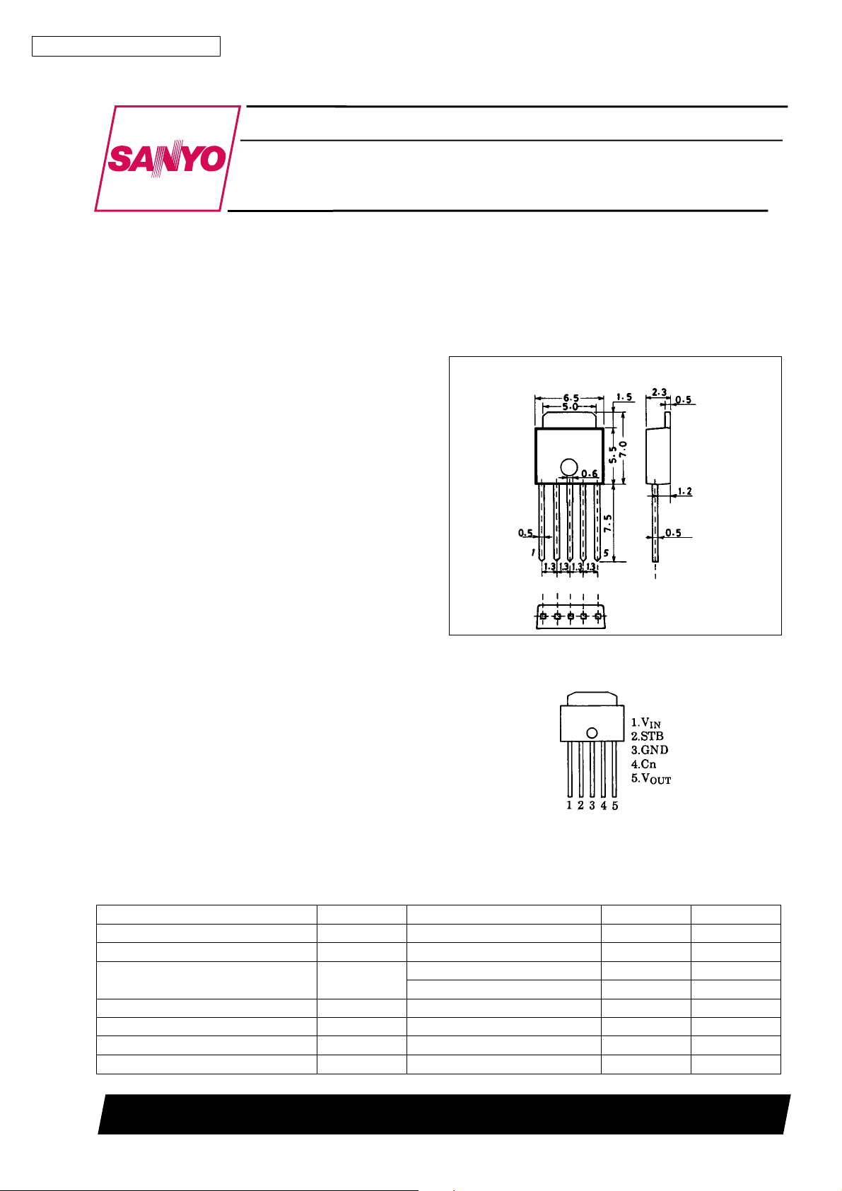
Package Dimensions
unit : mm
3103-TP-5H
[L88MS00T Series]
SANYO : TP-5H
Pin Assignment
Specifications
Maximum Ratings at Ta = 25°C (common to L88MS00T series)
Parameter Symbol Conditions Ratings Unit
Input voltage V
Strobe pin input voltage V
Allowable power dissipation Pd max Ta % 25°C, no heat sink 1 W
Thermal resistance (junction-atmosphere) θj-a 125 °C/W
Thermal resistance (junction-to-case) θj-c 20 °C/W
Operating temperature Topr –20 to +85 °C
Storage temperature Tstg –55 to +150 °C
ST
max
IN
max
Tc = 25°C, with infinite heat sink 6.25 W
18 V
VINmax V
SANYO Electric Co.,Ltd. Semiconductor Bussiness Headquarters
TOKYO OFFICE Tokyo Bldg., 1-10, 1 Chome, Ueno, Taito-ku, TOKYO, 110 JAPAN
31097HA(II)/9302TS No.4186-1/11
Top view
Page 2
[L88MS04T]
Operating Conditions atTa=25°C
Parameter Symbol Conditions Ratings Unit
Input voltage
Output current
Output on control voltage
Output off control voltage
L88MS00T Series
V
IN
l
OUT
V
STL
V
STH
4.7 to 17 V
0 to 500 mA
–0.3 to +0.8 V
2.0 to V
IN
V
Operating Characteristics at Tj = 25 °C, VIN=7V,IO= 500 mA, C
see specified Test Circuit.
Parameter Symbol Conditions min typ max Unit
[Output on, V
Output voltage V
Dropout voltage
Line regulation ∆V
Load regulation ∆V
Peak output current l
Output short-circuit current l
Quiescent current
Output noise voltage V
Temperature coefficient of
output voltage
Ripple rejection Rrej f = 120 Hz, 5 V % V
Output on control voltage V
[Output off, V
Low output voltage V
Static current I
Output off control voltage V
ST
ST
= ‘‘L’’]
= ‘‘H’’ ]
OUT
V
DROP1
V
DROP2lO
OLN
OLD
OP
OSC
I
Q1
I
Q2
NO
∆V
/∆Tj Tj = 25 to 125 °C ±0.4 mV/°C
OUT
STL
OFF VST= 5 V 20 200 mV
O
OFF VST= 5 V, Except I
Q
STH
= 150 mA 0.2 0.3 V
4.7 V % VIN% 17 V 10 50 mV
5mA%I
I
= 0 1.9 5.0 mA
OUT
% 500 mA 24 80 mV
OUT
10 Hz % f % 100 kHz 30 µVrms
% 17 V 72 dB
IN
STB
[L88MS05T]
Operating Conditions atTa=25°C
= 100 µF, CIN, Cn=1µF,
OUT
3.88 4.0 4.12 V
0.4 0.6 V
600 900 mA
100 300 mA
24 50 mA
35 70 µA
2.0 V
0.8 V
IN
V
Parameter Symbol Conditions Ratings Unit
Input voltage
Output current
Output on control voltage
Output off control voltage
l
V
V
V
IN
OUT
STL
STH
5.8 to 17 V
0 to 500 mA
–0.3 to +0.8 V
2.0 to V
IN
V
No.4186-2/11
Page 3
L88MS00T Series
Operating Characteristics at Tj = 25 °C, VIN=8V,IO= 500 mA, C
see specified Test Circuit.
Parameter Symbol Conditions min typ max Unit
[Output on, V
Output voltage V
Dropout voltage
Line regulation ∆V
Load regulation ∆V
Peak output current l
Output short-circuit current l
Quiescent current
Output noise voltage V
Temperature coefficient of
output voltage
Ripple rejection Rrej f = 120 Hz, 6 V % V
Output on control voltage V
[Output off, V
Low output voltage V
Static current I
Output off control voltage V
ST
ST
= ‘‘L’’]
= ‘‘H’’ ]
OUT
V
DROP1
V
DROP2lO
OLN
OLD
OP
OSC
I
Q1
I
Q2
NO
∆V
/∆Tj Tj = 25 to 125 °C ±0.5 mV/°C
OUT
STL
OFF VST= 5 V 20 200 mV
O
OFF VST= 5 V, Except I
Q
STH
= 150 mA 0.2 0.3 V
5.8 V % VIN% 17 V 10 50 mV
5mA%I
I
= 0 2.0 5.0 mA
OUT
% 500 mA 30 100 mV
OUT
10 Hz % f % 100 kHz 40 µVrms
% 17 V 74 dB
IN
STB
[L88MS06T]
Operating Conditions atTa=25°C
= 100 µF, CIN,Cn=1µF,
OUT
4.85 5.0 5.15 V
0.4 0.6 V
600 900 mA
100 300 mA
24 50 mA
40 80 µA
2.0 V
0.8 V
IN
V
Parameter Symbol Conditions Ratings Unit
Input voltage
Output current
Output on control voltage
Output off control voltage
l
V
V
V
IN
OUT
STL
STH
Operating Characteristics at Tj = 25 °C, VIN=9V,IO= 500 mA, C
see specified Test Circuit.
Parameter Symbol Conditions min typ max Unit
[Output on, V
Output voltage V
Dropout voltage
Line regulation ∆V
Load regulation ∆V
Peak output current l
Output short-circuit current l
Quiescent current
Output noise voltage V
Temperature coefficient of
output voltage
Ripple rejection Rrej f = 120 Hz, 7 V % V
Output on control voltage V
[Output off, V
Low output voltage V
Static current I
Output off control voltage V
ST
ST
= ‘‘L’’]
= ‘‘H’’ ]
OUT
V
DROP1
V
DROP2lO
OLN
OLD
OP
OSC
I
Q1
I
Q2
NO
∆V
/∆Tj Tj = 25 to 125 °C ±0.6 mV/°C
OUT
STL
OFF VST= 5 V 20 200 mV
O
OFF VST= 5 V, Except I
Q
STH
= 150 mA 0.2 0.3 V
6.8 V % VIN% 17 V 10 50 mV
5mA%I
I
= 0 2.1 5.0 mA
OUT
% 500 mA 36 120 mV
OUT
10 Hz % f % 100 kHz 40 µVrms
% 17 V 76 dB
IN
STB
6.8 to 17 V
0 to 500 mA
–0.3 to +0.8 V
2.0 to V
IN
= 100 µF, CIN,Cn=1µF,
OUT
5.82 6.0 6.18 V
0.4 0.6 V
600 900 mA
100 300 mA
24 50 mA
60 120 µA
2.0 V
V
0.8 V
IN
V
No.4186-3/11
Page 4

[L88MS08T]
Operating Conditions atTa=25°C
Parameter Symbol Conditions Ratings Unit
Input voltage
Output current
Output on control voltage
Output off control voltage
L88MS00T Series
V
IN
l
OUT
V
STL
V
STH
8.8 to 17 V
0 to 500 mA
–0.3 to +0.8 V
2.0 to V
IN
V
Operating Characteristics at Tj = 25 °C, VIN=11V,IO= 500 mA, C
see specified Test Circuit.
Parameter Symbol Conditions min typ max Unit
[Output on, V
Output voltage V
Dropout voltage
Line regulation ∆V
Load regulation ∆V
Peak output current l
Output short-circuit current l
Quiescent current
Output noise voltage V
Temperature coefficient of
output voltage
Ripple rejection Rrej f = 120 Hz, 9 V % V
Output on control voltage V
[Output off, V
Low output voltage V
Static current I
Output off control voltage V
ST
ST
= ‘‘L’’]
= ‘‘H’’ ]
OUT
V
DROP1
V
DROP2lO
OLN
OLD
OP
OSC
I
Q1
I
Q2
NO
∆V
/∆Tj Tj = 25 to 125 °C ±0.8 mV/°C
OUT
STL
OFF VST= 5 V 20 200 mV
O
OFF VST= 5 V, Except I
Q
STH
= 150 mA 0.2 0.3 V
8.8 V % VIN% 17 V 10 50 mV
5mA%I
I
= 0 2.2 5.0 mA
OUT
% 500 mA 48 160 mV
OUT
10 Hz % f % 100 kHz 40 µVrms
% 17 V 76 dB
IN
STB
[L88MS09T]
Operating Conditions atTa=25°C
= 100 µF, CIN,Cn=1µF,
OUT
7.76 8.0 8.24 V
0.4 0.6 V
600 900 mA
100 300 mA
24 50 mA
150 300 µA
2.0 V
0.8 V
IN
V
Parameter Symbol Conditions Ratings Unit
Input voltage
Output current
Output on control voltage
Output off control voltage
l
V
V
V
IN
OUT
STL
STH
9.9 to 17 V
0 to 500 mA
–0.3 to +0.8 V
2.0 to V
IN
V
No.4186-4/11
Page 5

L88MS00T Series
Operating Characteristics at Tj = 25 °C, VIN=12V,IO= 500 mA, C
see specified Test Circuit.
Parameter Symbol Conditions min typ max Unit
[Output on, V
Output voltage V
Dropout voltage
Line regulation ∆V
Load regulation ∆V
Peak output current l
Output short-circuit current l
Quiescent current
Output noise voltage V
Temperature coefficient of
output voltage
Ripple rejection Rrej f = 120 Hz, 10 V % V
Output on control voltage V
[Output off, V
Low output voltage V
Static current I
Output off control voltage V
ST
ST
= ‘‘L’’]
= ‘‘H’’ ]
OUT
V
DROP1
V
DROP2lO
OLN
OLD
OP
OSC
I
Q1
I
Q2
NO
∆V
/∆Tj Tj =25 to 125 °C ±0.9 mV/°C
OUT
STL
OFF VST= 5 V 20 200 mV
O
OFF VST= 5 V, Except I
Q
STH
= 150 mA 0.2 0.3 V
9.9 V % VIN% 17 V 10 50 mV
5mA%I
I
= 0 2.3 5.0 mA
OUT
% 500 mA 54 180 mV
OUT
10 Hz % f % 100 kHz 40 µVrms
% 17 V 76 dB
IN
STB
[L88MS12T]
Operating Conditions atTa=25°C
= 100 µF, CIN,Cn=1µF,
OUT
8.73 9.0 9.27 V
0.4 0.6 V
600 900 mA
100 300 mA
24 50 mA
200 400 µA
2.0 V
0.8 V
IN
V
Parameter Symbol Conditions Ratings Unit
Input voltage
Output current
Output on control voltage
Output off control voltage
l
V
V
V
IN
OUT
STL
STH
Operating Characteristics at Tj = 25 °C, VIN=15V,IO= 500 mA, C
see specified Test Circuit.
Parameter Symbol Conditions min typ max Unit
[Output on, V
Output voltage V
Dropout voltage
Line regulation ∆V
Load regulation ∆V
Peak output current l
Output short-circuit current l
Quiescent current
Output noise voltage V
Temperature coefficient of
output voltage
Ripple rejection Rrej f = 120 Hz, 13 V % V
Output on control voltage V
[Output off, V
Low output voltage V
Static current V
Output off control voltage V
ST
ST
= ‘‘L’’]
= ‘‘H’’ ]
OUT
V
DROP1
V
DROP2lO
OLN
OLD
OP
OSC
I
Q1
I
Q2
NO
∆V
/∆Tj Tj = 25 to 125 °C ±1.2 mV/°C
OUT
STL
OFF VST= 5 V 20 200 mV
O
OFF VST= 5 V, Except I
Q
STH
= 150 mA 0.2 0.3 V
13 V % VIN% 17 V 10 50 mV
5mA%I
I
= 0 2.6 5.0 mA
OUT
% 500 mA 70 240 mV
OUT
10 Hz % f % 100 kHz 40 µVrms
% 17 V 76 dB
IN
STB
13 to 17 V
0 to 500 mA
–0.3 to +0.8 V
2.0 to V
IN
= 100 µF, CIN,Cn=1µF,
OUT
11.64 12.0 12.36 V
0.4 0.6 V
600 900 mA
100 300 mA
24 50 mA
500 1000 µA
2.0 V
V
0.8 V
IN
V
No.4186-5/11
Page 6

L88MS00T Series
Equivalent Circuit Block Diagram
Error
amp
Start-up circuit
Test Circuit (Common to L88MS00T Series)
Reference voltage
ON/OFF
Control
Thermal protector
Short circuit
protector
L88MS00T
Notes: 1. Because the output capacitor C
exhibits little change in capacity with temperature variations should be used (such as a tantalum capacitor).
2. Adding capacitor Cn enables external noise suppression and ripple rejection to be improved. However, attention should
be given to system stability (phase margin).
3. To ensure operational stability, C
4. When the strobe (STB) pin is open, output is turned on by internal bias. When the strobe function is not used, the STB
pin should be connected to GND to complete strobe operation.
5. When V
is minus (–) and GND is plus (+) (reversed connection), excessive current flow will occur.
IN
is set at over 100 µF to prevent oscillation at low temperatures, a capacitor that
OUT
IN,COUT
, and Cn should be placed as close to the IC as possible.
No.4186-6/11
Page 7

L88MS00T Series
Function Table On/off Control Input Equivalent Circuit
V
STB
V
OUT
LH
HL
Sample Application Circuit
Adjustment of output voltage V
(1) Reducing V
V
OUT
R
A
(2) Increasing V
V
OUT
OUT
can be lowered by externally connecting a resistor
between the Cn and V
OUT
can be raised by externally connecting a resistor R
between the Cn and GND pins.
OUT
OUT
pins.
Control
signal
B
Pd max – Ta
Common for L88MS00T Series
With infinite heat sink
Mounted on copper-clad
area of 2,000mm
Mounted on copper-clad
area 740 mm
Mounted on copper-clad
area 180 mm
Mounted on copper-clad
area 36 mm
No heat sink
Allowable power dissipation, Pd max – W
2
2
2
2
Ambient temperature, Ta – °C
The allowable power dissipation is 1.0 W (Ta = 25°C) with no fin attached, but when mounted on a hybrid IC board or printed
circuit board, high allowable power dissipation is achieved, despite the compact package. The graph below depicts the relationship
between the copper-clad area and allowable power dissipation when mounted on a glass epoxy board (50 × 50×0.8 tmm
3
) with a
copper thickness of 18 µm.
No.4186-7/11
Page 8

L88MS00T Series
Pd max – S
Common for L88MS00T series
Allowable power dissipation, Pd max – W
Copper-clad area,S–mm
2
* Pd is the value for when the solder on the surface of the IC heat sink has melted completely and the surface mount is
horizontal.
* Please be advised that the flow solder application system (full-heat method) cannot be recommended.
Lead Formings
MA forming
LR forming
FA forming
–V
O
Output voltage, V
VO–V
IN
Input voltage, VIN–V
–V
O
Output voltage, V
VO–V
Input voltage, V
IN
–V
IN
No.4186-8/11
Page 9

L88MS00T Series
–V
O
Output voltage, V
–V
O
VO–V
IN
Input voltage, VIN–V
VO–I
O
–V
DROP
Dropout voltage, V
–V
O
V
DROP–IO
Common for L88MS00T Series
Output current, IO–A
VO–I
O
Output voltage, V
–V
O
Output voltage, V
–mA
Q
Output current, IO–A
VO–V
ST
Strobe voltage, VST–V
IQ–V
IN
–V
STH
Output off control voltage, V
Output voltage, V
–V
STL
Output on control voltage, V
–mA
Q
Output current, I
V
STH,VSTL
Common for L88MS00T Series
O
–Ta
–A
Ambient temperature, Ta – °C
IQ–V
IN
Quiescent current, I
Input voltage, VIN–V
Quiescent current, I
Input voltage, VIN–V
No.4186-9/11
Page 10

L88MS00T Series
–mA
Q
Quiescent current, I
–V
O
I
Q–IO
Output current, IO–A
V
–Ta
O
–mA
Q OFF
Quiescent current during strobe, I
–mA
Q
I
Q OFF (ST ON)–VIN
(except IST)
Input voltage, V
IQ–Ta
–V
IN
Output voltage, V
–A
OP
Peak output current, I
–A
OSC
Output short-circuit current, I
Ambient temperature, Ta – °C
IOP,I
–Ta
OSC
Common for L88MS00T Series
Ambient temperature, Ta – °C
Rrej – f
Quiescent current, I
–mA
Q OFF
Quiescent current during strobe, I
Ambient temperature, Ta – °C
I
Q OFF (ST ON)
–Ta
Ambient temperature, Ta – °C
(except I
ST
)
Ripple rejection, Rrej – dB
Frequency,f–Hz
No.4186-10/11
Page 11

L88MS00T Series
No products described or contained herein are intended for use in surgical implants, life-support systems, aerospace equipment,
nuclear power control systems, vehicles, disaster/crime-prevention equipment and the like, the failure of which may directly or
indirectly cause injury, death or property loss.
Anyone purchasing any products described or contained herein for an above-mentioned use shall:
1 Accept full responsibility and indemnify and defend SANYO ELECTRIC CO., LTD., its affiliates, subsidiaries and distributors
and all their officers and employees, jointly and severally, against any and all claims and litigation and all damages, cost and
expenses associated with such use:
2 Not impose any responsibility for any fault or negligence which may be cited in any such claim or litigation on SANYO
ELECTRIC CO., LTD., its affiliates, subsidiaries and distributors or any of their officers and employees jointly or severally.
Information (including circuit diagrams and circuit parameters) herein is for example only; it is not guaranteed for volume
production. SANYO believes information herein is accurate and reliable, but no guarantees are made or implied regarding its use
or any infringements of intellectual property rights or other rights of third parties.
This catalog provides information as of March, 1997. Specifications and information herein are subject to change without notice.
No.4186-11/11
 Loading...