

Page 1
General Description
KSZ8893FQL
Single-Chip 3-Port Switch
with Fiber Support
Rev. 1.3
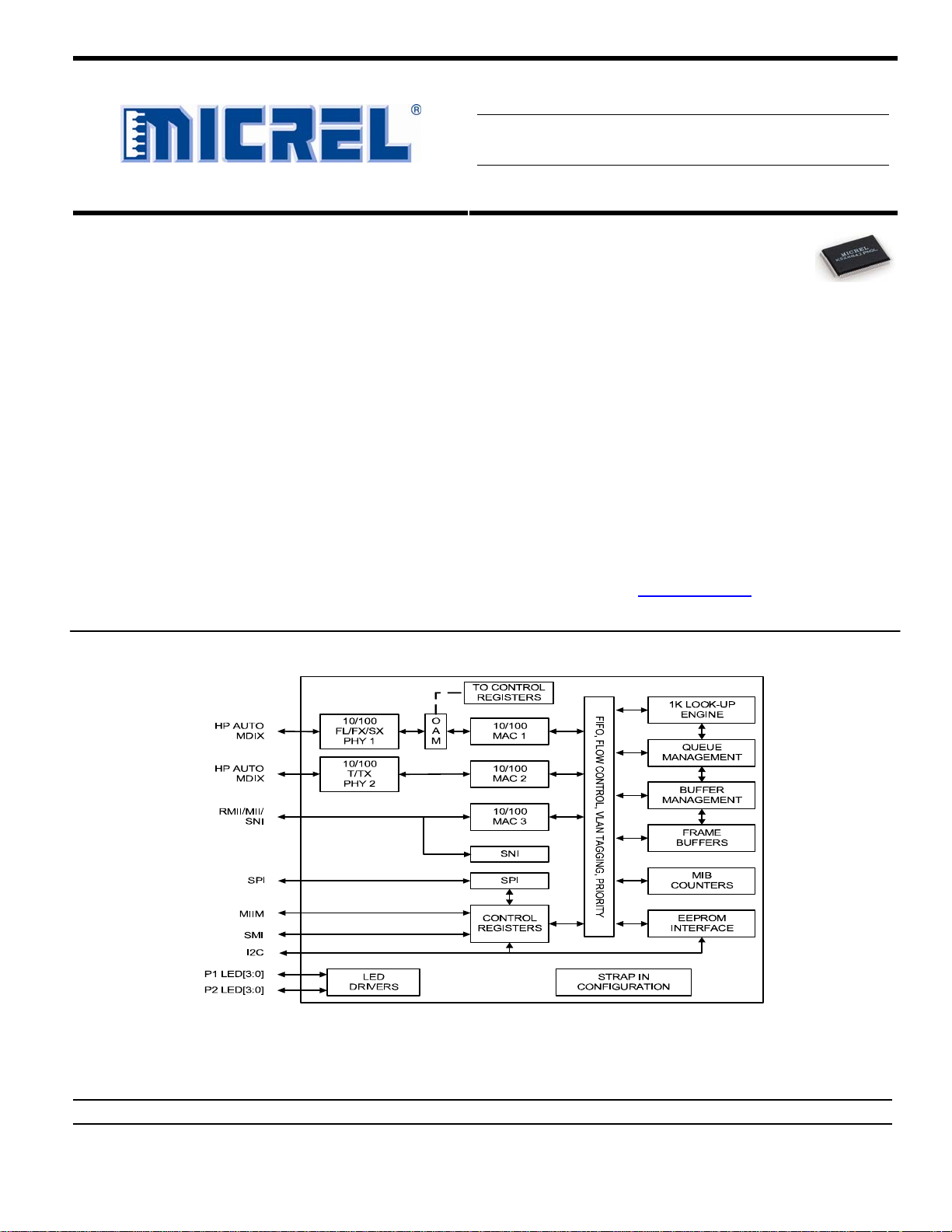
The KSZ8893FQL, a highly integrated single-chip 3 port
Fast Ethernet switch is designed for applications with
fiber support such as media converter. It provides two
10/100 transceivers with patented mixed-signal lowpower technology, three media access control (MAC)
units, a high-speed non-blocking switch fabric, a Layer-2
managed switch and TS-1000 OAM (Operations,
Administration and Management) V2 in a compact
solution. Backwards compatible to the TS-1000 (2002)
specification, TS-1000 V2 is an OAM sub-layer that
provides communication between CO (central office) and
CPE (customer premises equipment).
In fiber mode, one PHY unit can be configurable to
100Base-FX, 100Base-SX, or 10Base-FL fiber for
conversion to 10Base-T and 100Base-TX copper. A fiber
LED driver and post amplifier are also included for
10Base-FL and 100Base-SX applications.
Functional Diagram
LinkMD®
In copper mode, both PHY units support 10Base-T and
100Base-TX with HP Auto MDI/MDI-X for reliable
detection of and correction for straight-through and
crossover cables, and LinkMD
diagnostics for identification of faulty cabling.
The high performance switching engine features an
extensive feature set that includes programmable rate
limiting, tag/port-based VLAN, 4 priority class,
RMII/MII/SNI and CPU control/data interfaces to
effectively address both current and emerging Fast
Ethernet applications.
The KSZ8893FQL comes in a lead-free package (see
Ordering Information).
Data sheets and support documentation can be found on
Micrel’s web site at: www.micrel.com
®
TDR-based cable
.
KSZ8893FQL
LinkMD is a registered trademark of Micrel, Inc
Product/Application names used in this datasheet are for identification purposes only and may be trademarks of their respective companies.
Micrel Inc. • 2180 Fortune Drive • San Jose, CA 95131 • USA • tel +1 (408) 944-0800 • fax + 1 (408) 474-1000 • http://www.micrel.com
October 2007
M9999-101607-1.3
Page 2

Micrel, Inc. KSZ8893FQL
Features
Integrated 3-Port 10/100 Ethernet Switch
• Three MACs and two PHYs fully compliant with IEEE
802.3u standard
• Non-blocking switch fabric assures fast packet
delivery by utilizing an 1K MAC address lookup table
• Control registers configurable on the fly (port-priority,
802.1p/d/q, AN…)
QoS/CoS Packet Prioritization Support
• Per port, 802.1p and DiffServ-based
• Re-mapping of 802.1p priority field per port basis
• Four priority levels
and a store-and-forward architecture
• Full duplex IEEE 802.3x flow control (PAUSE) with
force mode option
• Half-duplex back pressure flow control
• HP Auto MDI-X for reliable detection of and correction
for straight-through and crossover cables with disable
and enable option
®
• Micrel LinkMD
TDR-based cable diagnostics permit
identification of faulty copper cabling
• 100Base-FX, 100Base-SX and 10Base-FL fiber
support on port 1
• MII interface supports both MAC mode and PHY mode
• RMII interface support with external 50MHz system
clock
• 7-wire serial network interface (SNI) support for legacy
MAC
• Comprehensive LED Indicator support for link, activity,
full/half duplex and 10/100 speed
Fiber Support
• Integrated LED driver and post amplifier for 10BaseFL and 100Base-SX optical modules
TTC TS-1000 OAM
• Supports OAM sub-layer which conforms to TS-1000
V2 specification from TTC (Telecommunication
Technology Committee)
• Sends and receives OAM frames to Center or
Terminal side
Advanced Switch Features
• IEEE 802.1q VLAN support for up to 16 groups (fullrange of VLAN IDs)
• VLAN ID tag/untag options, per port basis
• IEEE 802.1p/q tag insertion or removal on a per port
basis (egress)
• Programmable rate limiting at the ingress and egress
on a per port basis
• Broadcast storm protection with % control (global and
per port basis)
• IEEE 802.1d spanning tree protocol support
• Special tagging mode to inform the processor which
ingress port receives the packet
• IGMP snooping (Ipv4) and MLD snooping (Ipv6)
support for multicast packet filtering
• MAC filtering function to forward unknown unicast
packets to specified port
• Double-tagging support
Low Latency Support
• Repeater mode
Switch Monitoring Features
• Port mirroring/monitoring/sniffing: ingress and/or
egress traffic to any port or MII
• MIB counters for fully compliant statistics gathering, 34
MIB counters per port
• Loopback modes for remote diagnostic of failure
• Loop back mode to support loop back packet from
Center side to Terminal side
• Far-end fault detection with disable and enable
• Link Transparency to indicate link down from link
partner
• Unique User Defined Register (UDR) feature brings
OAM to low cost/complexity nodes
Comprehensive Configuration Register Access
2
• SMI, SPI and I
C management interfaces to all 8-bit
internal registers
Low Power Dissipation
• Full-chip hardware power-down (register configuration
not saved)
• Per port based software power-save on PHY (idle link
detection, register configuration preserved)
• Voltages:
– Core 1.2V
– I/O and Transceiver 3.3V
Available in 128-Pin PQFP, Lead-free package
• MII management (MIIM) interface to PHY registers
• I/O pins strapping and EEPROM to program selective
registers in unmanaged switch mode
October 2007
2
M9999-101607-1.3
Page 3

Micrel, Inc. KSZ8893FQL
Applications
• Media Conversion Modules:
– 10Base-FL <=> 10Base-T
– 100Base-SX <=> 100Base-TX
– 100Base-FX <=> 100Base-TX
• FTTx Managed/Unmanaged Media Converters
• Fiber Broadband Gateways
Ordering Information
Part Number Temp. Range Package Lead Finish Description
KSZ8893FQL 0°C to 70°C 128-Pin PQFP Pb-Free
KSZ8893FQL-FX 0°C to 70°C 128-Pin PQFP Pb-Free Port 1 supports 100Base-FX with TS-1000 OAM V2
Port 1 supports 10Base-FL and 100Base-SX with LED
driver and post amp
October 2007
3
M9999-101607-1.3
Page 4

Micrel, Inc. KSZ8893FQL
Revision History
Revision Date Summary of Changes
1.0 07/05/06 Data sheet created.
1.1 02/08/07 Modify Table 10. RMII Signal Connections
Add TLA-6T718 to Table 37. Qualified Single Port Magnetics
Remove KSZ8893FQLI from the datasheet
1.2 06/19/07 Update Ordering Information
Add Thermal Resistance (θ
1.3 10/16/07 Recommend connecting a 100ohm resistor between VDDC and 3.3V power rail.
) to Operating Rating
JC
October 2007
4
M9999-101607-1.3
Page 5

Micrel, Inc. KSZ8893FQL
Contents
Pin Configuration............................................................................................................................................................12
Pin Description................................................................................................................................................................13
Functional Description ...................................................................................................................................................22
Functional Overview: Media Conversion......................................................................................................................22
TS-1000 OAM Operation............................................................................................................................................ 22
OAM Frame Format .............................................................................................................................................22
Media Converter Modes.......................................................................................................................................24
MC Loop Back Operation.....................................................................................................................................25
Dedicated TS-1000 Registers & Pins...................................................................................................................26
10Base-FL Operation .................................................................................................................................................27
Physical Interface.................................................................................................................................................27
Enabling 10Base-FL Mode...................................................................................................................................27
100Base-SX Operation............................................................................................................................................... 27
Physical Interface.................................................................................................................................................27
Enabling 100Base-SX Mode................................................................................................................................27
100Base-TX Transmit................................................................................................................................................. 28
100Base-TX Receive.................................................................................................................................................. 28
PLL Clock Synthesizer................................................................................................................................................ 28
Scrambler/De-scrambler (100Base-TX Only)............................................................................................................. 28
100Base-FX Operation ............................................................................................................................................... 29
100Base-FX Signal Detection.....................................................................................................................................29
100Base-FX Far-End Fault.........................................................................................................................................29
10Base-T Transmit ..................................................................................................................................................... 29
10Base-T Receive ...................................................................................................................................................... 29
Fiber LED Driver .........................................................................................................................................................29
Post Amplifier.............................................................................................................................................................. 30
Power Management.................................................................................................................................................... 30
MDI/MDI-X Auto Crossover ........................................................................................................................................ 30
Straight Cable.......................................................................................................................................................30
Crossover Cable...................................................................................................................................................31
Auto-Negotiation .........................................................................................................................................................32
LinkMD Cable Diagnostics.......................................................................................................................................... 33
Access..................................................................................................................................................................33
Usage...................................................................................................................................................................33
Functional Overview: MAC and Switch.........................................................................................................................34
Address Lookup.......................................................................................................................................................... 34
Learning...................................................................................................................................................................... 34
Migration .....................................................................................................................................................................34
Aging...........................................................................................................................................................................34
Forwarding.................................................................................................................................................................. 34
Switching Engine ........................................................................................................................................................ 37
MAC Operation ...........................................................................................................................................................37
Inter Packet Gap (IPG).........................................................................................................................................37
Back-Off Algorithm...............................................................................................................................................37
Late Collision........................................................................................................................................................37
Illegal Frames.......................................................................................................................................................37
Full Duplex Flow Control......................................................................................................................................37
Half-Duplex Backpressure ...................................................................................................................................37
Broadcast Storm Protection.................................................................................................................................38
MII Interface Operation ............................................................................................................................................... 38
RMII Interface Operation ............................................................................................................................................39
SNI (7-Wire) Operation ............................................................................................................................................... 40
MII Management (MIIM) Interface .............................................................................................................................. 41
Serial Management Interface (SMI)............................................................................................................................ 41
October 2007
5
M9999-101607-1.3
Page 6

Micrel, Inc. KSZ8893FQL
Repeater Mode ...........................................................................................................................................................42
Advanced Switch Functions..........................................................................................................................................42
Spanning Tree Support............................................................................................................................................... 42
Special Tagging Mode ................................................................................................................................................ 43
IGMP Support .............................................................................................................................................................44
IGMP Snooping....................................................................................................................................................44
Multicast Address Insertion in the Static MAC Table...........................................................................................44
IPv6 MLD Snooping.................................................................................................................................................... 44
Port Mirroring Support ................................................................................................................................................44
IEEE 802.1Q VLAN Support....................................................................................................................................... 45
QoS Priority Support................................................................................................................................................... 46
Port-Based Priority...................................................................................................................................................... 46
802.1p-Based Priority ................................................................................................................................................. 46
DiffServ-Based Priority ...............................................................................................................................................47
Rate Limiting Support ................................................................................................................................................. 47
Unicast MAC Address Filtering................................................................................................................................... 47
Configuration Interface ...............................................................................................................................................47
I2C Master Serial Bus Configuration....................................................................................................................47
I2C Slave Serial Bus Configuration......................................................................................................................48
SPI Slave Serial Bus Configuration......................................................................................................................49
Loopback Support....................................................................................................................................................... 52
Far-end Loopback................................................................................................................................................52
Near-end (Remote) Loopback..............................................................................................................................53
MII Management (MIIM) Registers .................................................................................................................................54
PHY1 Register 0 (PHYAD = 0x1, REGAD = 0x0): MII Basic Control......................................................................... 55
PHY2 Register 0 (PHYAD = 0x2, REGAD = 0x0): MII Basic Control......................................................................... 55
PHY1 Register 1 (PHYAD = 0x1, REGAD = 0x1): MII Basic Status ..........................................................................56
PHY2 Register 1 (PHYAD = 0x2, REGAD = 0x1): MII Basic Status ..........................................................................56
PHY1 Register 2 (PHYAD = 0x1, REGAD = 0x2): PHYID High................................................................................. 56
PHY2 Register 2 (PHYAD = 0x2, REGAD = 0x2): PHYID High................................................................................. 56
PHY1 Register 3 (PHYAD = 0x1, REGAD = 0x3): PHYID Low..................................................................................56
PHY2 Register 3 (PHYAD = 0x2, REGAD = 0x3): PHYID Low..................................................................................56
PHY1 Register 4 (PHYAD = 0x1, REGAD = 0x4): Auto-Negotiation Advertisement Ability.......................................57
PHY2 Register 4 (PHYAD = 0x2, REGAD = 0x4): Auto-Negotiation Advertisement Ability.......................................57
PHY1 Register 5 (PHYAD = 0x1, REGAD = 0x5): Auto-Negotiation Link Partner Ability ..........................................57
PHY2 Register 5 (PHYAD = 0x2, REGAD = 0x5): Auto-Negotiation Link Partner Ability ..........................................57
PHY1 Register 29 (PHYAD = 0x1, REGAD = 0x1D): LinkMD Control/Status ...........................................................58
PHY2 Register 29 (PHYAD = 0x2, REGAD = 0x1D): LinkMD Control/Status ...........................................................58
PHY1 Register 31 (PHYAD = 0x1, REGAD = 0x1F): PHY Special Control/Status.................................................... 58
PHY2 Register 31 (PHYAD = 0x2, REGAD = 0x1F): PHY Special Control/Status.................................................... 58
Global Registers ......................................................................................................................................................... 60
Register 0 (0x00): Chip ID0..................................................................................................................................60
Register 1 (0x01): Chip ID1 / Start Switch ...........................................................................................................60
Register 2 (0x02): Global Control 0......................................................................................................................61
Register 3 (0x03): Global Control 1......................................................................................................................61
Register 4 (0x04): Global Control 2......................................................................................................................62
Register 5 (0x05): Global Control 3......................................................................................................................63
Register 6 (0x06): Global Control 4......................................................................................................................63
Register 7 (0x07): Global Control 5......................................................................................................................64
Register 8 (0x08): Global Control 6......................................................................................................................64
Register 9 (0x09): Global Control 7......................................................................................................................64
Register 10 (0x0A): Global Control 8...................................................................................................................65
Register 11 (0x0B): Global Control 9...................................................................................................................65
Register 12 (0x0C): Global Control 10.................................................................................................................65
Register 13 (0x0D): Global Control 11.................................................................................................................66
October 2007
6
M9999-101607-1.3
Page 7

Micrel, Inc. KSZ8893FQL
Register 14 (0x0E): Global Control 12.................................................................................................................66
Register 15 (0x0F): Global Control 13 .................................................................................................................66
Port Registers .............................................................................................................................................................67
Register 16 (0x10): Port 1 Control 0 ....................................................................................................................67
Register 32 (0x20): Port 2 Control 0 ....................................................................................................................67
Register 48 (0x30): Port 3 Control 0 ....................................................................................................................67
Register 17 (0x11): Port 1 Control 1 ....................................................................................................................68
Register 33 (0x21): Port 2 Control 1 ....................................................................................................................68
Register 49 (0x31): Port 3 Control 1 ....................................................................................................................68
Register 18 (0x12): Port 1 Control 2 ....................................................................................................................69
Register 34 (0x22): Port 2 Control 2 ....................................................................................................................69
Register 50 (0x32): Port 3 Control 2 ....................................................................................................................69
Register 19 (0x13): Port 1 Control 3 ....................................................................................................................69
Register 35 (0x23): Port 2 Control 3 ....................................................................................................................69
Register 51 (0x33): Port 3 Control 3 ....................................................................................................................69
Register 20 (0x14): Port 1 Control 4 ....................................................................................................................70
Register 36 (0x24): Port 2 Control 4 ....................................................................................................................70
Register 52 (0x34): Port 3 Control 4 ....................................................................................................................70
Register 21 (0x15): Port 1 Control 5 ....................................................................................................................70
Register 37 (0x25): Port 2 Control 5 ....................................................................................................................70
Register 53 (0x35): Port 3 Control 5 ....................................................................................................................70
Register 22 (0x16): Port 1 Control 6 ....................................................................................................................71
Register 38 (0x26): Port 2 Control 6 ....................................................................................................................71
Register 54 (0x36): Port 3 Control 6 ....................................................................................................................71
Register 23 (0x17): Port 1 Control 7 ....................................................................................................................72
Register 39 (0x27): Port 2 Control 7 ....................................................................................................................72
Register 55 (0x37): Port 3 Control 7 ....................................................................................................................72
Register 24 (0x18): Port 1 Control 8 ....................................................................................................................73
Register 40 (0x28): Port 2 Control 8 ....................................................................................................................73
Register 56 (0x38): Port 3 Control 8 ....................................................................................................................73
Register 25 (0x19): Port 1 Control 9 ....................................................................................................................74
Register 41 (0x29): Port 2 Control 9 ....................................................................................................................74
Register 57 (0x39): Port 3 Control 9 ....................................................................................................................74
Register 26 (0x1A): Port 1 PHY Special Control/Status ......................................................................................75
Register 42 (0x2A): Port 2 PHY Special Control/Status ......................................................................................75
Register 58 (0x3A): Reserved, not applied to port 3............................................................................................75
Register 27 (0x1B): Port 1 LinkMD Result...........................................................................................................75
Register 43 (0x2B): Port 2 LinkMD Result...........................................................................................................75
Register 59 (0x3B): Reserved, not applied to port 3............................................................................................75
Register 28 (0x1C): Port 1 Control 12..................................................................................................................76
Register 44 (0x2C): Port 2 Control 12..................................................................................................................76
Register 60 (0x3C): Reserved, not applied to port 3............................................................................................76
Register 29 (0x1D): Port 1 Control 13..................................................................................................................77
Register 45 (0x2D): Port 2 Control 13..................................................................................................................77
Register 61 (0x3D): Reserved, not applied to port 3............................................................................................77
Register 30 (0x1E): Port 1 Status 0 .....................................................................................................................77
Register 46 (0x2E): Port 2 Status 0 .....................................................................................................................77
Register 62 (0x3E): Reserved, not applied to port 3............................................................................................77
Register 31 (0x1F): Port 1 Status 1......................................................................................................................78
Register 47 (0x2F): Port 2 Status 1......................................................................................................................78
Register 63 (0x3F): Port 3 Status 1......................................................................................................................78
TS-1000 Media Converter Registers ..........................................................................................................................79
Register 64 (0x40): PHY Address........................................................................................................................79
Register 65 (0x41): Center Side Status ...............................................................................................................79
Register 66 (0x42): Center Side Command.........................................................................................................80
October 2007
7
M9999-101607-1.3
Page 8

Micrel, Inc. KSZ8893FQL
Register 67 (0x43): PHY-SW Initialize.................................................................................................................80
Register 68 (0x44): Loop Back Setup1................................................................................................................81
Register 69 (0x45): Loop Back Setup2................................................................................................................82
Register 70 (0x46): Loop Back Result Counter for CRC Error ............................................................................82
Register 71 (0x47): Loop Back Result Counter for Timeout................................................................................82
Register 72 (0x48): Loop Back Result Counter for Good Packet........................................................................83
Register 73 (0x49): Additional Status (Center and Terminal side) ......................................................................83
Register 74 (0x4A): Remote Command 1............................................................................................................84
Register 75 (0x4B): Remote Command 2............................................................................................................84
Register 76 (0x4C): Remote Command 3............................................................................................................85
Register 77 (0x4D): Valid MC Packet Transmitted Counter ................................................................................85
Register 78 (0x4E): Valid MC Packet Received Counter.....................................................................................85
Register 79 (0x4F): Shadow of 0x58h Register...................................................................................................85
Register 80 (0x50): My Status 1 (Terminal and Center side) ..............................................................................86
Register 81 (0x51): My Status 2...........................................................................................................................86
Register 82 (0x52): My Vendor Info (1)................................................................................................................87
Register 83 (0x53): My Vendor Info (2)................................................................................................................87
Register 84 (0x54): My Vendor Info (3)................................................................................................................87
Register 85 (0x55): My Model Info (1)..................................................................................................................87
Register 86 (0x56): My Model Info (2)..................................................................................................................87
Register 87 (0x57): My Model Info (3)..................................................................................................................87
Register 88 (0x58): LNK Partner Status (1).........................................................................................................88
Register 89 (0x59): LNK Partner Status (2).........................................................................................................88
Register 90 (0x5A): LNK Partner Vendor Info (1)................................................................................................88
Register 91 (0x5B): LNK Partner Vendor Info (2)................................................................................................88
Register 92 (0x5C): LNK Partner Vendor Info (3)................................................................................................88
Register 93 (0x5D): LNK Partner Model Info (1)..................................................................................................88
Register 94 (0x5E): LNK Partner Model Info (2)..................................................................................................88
Register 95 (0x5F): LNK Partner Model Info (3)..................................................................................................88
Advanced Control Registers ....................................................................................................................................... 89
Register 96 (0x60): TOS Priority Control Register 0............................................................................................89
Register 97 (0x61): TOS Priority Control Register 1............................................................................................89
Register 98 (0x62): TOS Priority Control Register 2............................................................................................89
Register 99 (0x63): TOS Priority Control Register 3............................................................................................89
Register 100 (0x64): TOS Priority Control Register 4..........................................................................................90
Register 101 (0x65): TOS Priority Control Register 5..........................................................................................90
Register 102 (0x66): TOS Priority Control Register 6..........................................................................................90
Register 103 (0x67): TOS Priority Control Register 7..........................................................................................90
Register 104 (0x68): TOS Priority Control Register 8..........................................................................................91
Register 105 (0x69): TOS Priority Control Register 9..........................................................................................91
Register 106 (0x6A): TOS Priority Control Register 10 .......................................................................................91
Register 107 (0x6B): TOS Priority Control Register 11 .......................................................................................91
Register 108 (0x6C): TOS Priority Control Register 12.......................................................................................92
Register 109 (0x6D): TOS Priority Control Register 13.......................................................................................92
Register 110 (0x6E): TOS Priority Control Register 14 .......................................................................................92
Register 111 (0x6F): TOS Priority Control Register 15........................................................................................92
Switch MAC Address Registers.................................................................................................................................. 93
Register 112 (0x70): MAC Address Register 0....................................................................................................93
Register 113 (0x71): MAC Address Register 1....................................................................................................93
Register 114 (0x72): MAC Address Register 2....................................................................................................93
Register 115 (0x73): MAC Address Register 3....................................................................................................93
Register 116 (0x74): MAC Address Register 4....................................................................................................93
Register 117 (0x75): MAC Address Register 5....................................................................................................93
User Defined Registers............................................................................................................................................... 93
Register 118 (0x76): User Defined Register 1.....................................................................................................93
October 2007
8
M9999-101607-1.3
Page 9

Micrel, Inc. KSZ8893FQL
Register 119 (0x77): User Defined Register 2.....................................................................................................93
Register 120 (0x78): User Defined Register 3.....................................................................................................93
Indirect Access Registers ........................................................................................................................................... 94
Register 121 (0x79): Indirect Access Control 0 ...................................................................................................94
Register 122 (0x7A): Indirect Access Control 1...................................................................................................94
Register 123 (0x7B): Indirect Data Register 8.....................................................................................................94
Register 124 (0x7C): Indirect Data Register 7.....................................................................................................94
Register 125 (0x7D): Indirect Data Register 6.....................................................................................................94
Register 126 (0x7E): Indirect Data Register 5.....................................................................................................94
Register 127 (0x7F): Indirect Data Register 4 .....................................................................................................94
Register 128 (0x80): Indirect Data Register 3......................................................................................................95
Register 129 (0x81): Indirect Data Register 2......................................................................................................95
Register 130 (0x82): Indirect Data Register 1......................................................................................................95
Register 131 (0x83): Indirect Data Register 0......................................................................................................95
Reserved Registers .................................................................................................................................................... 95
Register 132 (0x84): Digital Testing Status 0 ......................................................................................................95
Register 133 (0x85): Digital Testing Control 0.....................................................................................................95
Register 134 (0x86): Analog Testing Control 0....................................................................................................95
Register 135 (0x87): Analog Testing Control 1....................................................................................................95
Register 136 (0x88): Analog Testing Control 2....................................................................................................95
Register 137 (0x89): Analog Testing Control 3....................................................................................................96
Register 138 (0x8A): Analog Testing Status........................................................................................................96
Register 139 (0x8B): Analog Testing Control 4 ...................................................................................................96
Register 140 (0x8C): QM Debug 1.......................................................................................................................96
Register 141 (0x8D): QM Debug 2.......................................................................................................................96
Static MAC Address Table.......................................................................................................................................... 97
VLAN Table.................................................................................................................................................................99
Dynamic MAC Address Table................................................................................................................................... 100
MIB (Management Information Base) Counters....................................................................................................... 101
Additional MIB Counter Information...................................................................................................................103
Absolute Maximum Ratings
Operating Ratings
(2)
......................................................................................................................................................104
Electrical Characteristics
(1)
......................................................................................................................................104
(4)
..........................................................................................................................................104
Timing Diagrams...........................................................................................................................................................106
EEPROM Timing ......................................................................................................................................................106
SNI Timing ................................................................................................................................................................107
MII Timing .................................................................................................................................................................108
RMII Timing...............................................................................................................................................................109
SPI Input Timing .......................................................................................................................................................110
SPI Output Timing ....................................................................................................................................................111
Auto-Negotiation Timing ...........................................................................................................................................112
October 2007
9
M9999-101607-1.3
Page 10

Micrel, Inc. KSZ8893FQL
List of Figures
Figure 1. TS-1000 OAM Frame Format ...........................................................................................................................23
Figure 2. Typical TS-1000 Media Converter Application .................................................................................................24
Figure 3. KSZ8893FQL MC Loop Back Paths .................................................................................................................25
Figure 4. Typical Straight Cable Connection ................................................................................................................... 31
Figure 5. Typical Crossover Cable Connection ...............................................................................................................31
Figure 6. Auto-Negotiation and Parallel Operation. ......................................................................................................... 32
Figure 7. Destination Address Lookup Flow Chart, Stage 1............................................................................................ 35
Figure 8. Destination Address Resolution Flow Chart, Stage 2....................................................................................... 36
Figure 9. 802.1p Priority Field Format..............................................................................................................................46
Figure 10. KSZ8893FQL EEPROM Configuration Timing Diagram. ............................................................................... 48
Figure 11. SPI Write Data Cycle. ..................................................................................................................................... 50
Figure 12. SPI Read Data Cycle. ..................................................................................................................................... 50
Figure 13. SPI Multiple Write. ..........................................................................................................................................51
Figure 14. SPI Multiple Read. .......................................................................................................................................... 51
Figure 15. Far-End Loopback Path. ................................................................................................................................. 52
Figure 16. Near-end (Remote) Loopback Path................................................................................................................ 53
Figure 17. EEPROM Interface Input Timing Diagram.................................................................................................... 106
Figure 18. EEPROM Interface Output Timing Diagram ................................................................................................. 106
Figure 19. SNI Timing – Data Received from SNI ......................................................................................................... 107
Figure 20. SNI Timing – Data Input-to-SNI ....................................................................................................................107
Figure 21. MII Timing – Data Received from MII ........................................................................................................... 108
Figure 22. MII Timing – Data Input-to-MII ......................................................................................................................108
Figure 23. RMII Timing – Data Received from RMII ......................................................................................................109
Figure 24. RMII Timing – Data Input-to-RMII................................................................................................................. 109
Figure 25. SPI Input Timing ...........................................................................................................................................110
Figure 26. SPI Output Timing......................................................................................................................................... 111
Figure 27. Auto-Negotiation Timing ...............................................................................................................................112
Figure 28. Reset Timing ................................................................................................................................................. 113
Figure 29. Recommended Reset Circuit........................................................................................................................ 114
Figure 30. Recommended Reset Circuit for interfacing with CPU/FPGA Reset Output................................................ 114
October 2007
10
M9999-101607-1.3
Page 11

Micrel, Inc. KSZ8893FQL
List of Tables
Table 1. TS-1000 Media Converter Mode Selection........................................................................................................ 24
Table 2. Dedicated TS-1000 Pins ....................................................................................................................................26
Table 3. 10Base-FL Configuration ................................................................................................................................... 27
Table 4. 100Base-SX Configuration................................................................................................................................. 28
Table 5. FX and TX Mode Selection ................................................................................................................................ 29
Table 6. Programmable Current Values for Fiber LED Driver .........................................................................................30
Table 7. MDI/MDI-X Pin Definitions .................................................................................................................................30
Table 8. MII Signals.......................................................................................................................................................... 38
Table 9. RMII Signal Description...................................................................................................................................... 39
Table 10. RMII Signal Connections.................................................................................................................................. 40
Table 11. SNI Signals....................................................................................................................................................... 40
Table 12. MII Management Interface Frame Format .......................................................................................................41
Table 13. Serial Management Interface (SMI) Frame Format .........................................................................................41
Table 14. Spanning Tree States ......................................................................................................................................42
Table 15. Special Tagging Mode Format ......................................................................................................................... 43
Table 16. STPID Egress Rules (Processor to Switch Port 3) .......................................................................................... 43
Table 17. STPID Egress Rules (Switch Port 3 to Processor) ..........................................................................................44
Table 18. FID+DA Lookup in VLAN Mode .......................................................................................................................45
Table 19. FID+SA Lookup in VLAN Mode .......................................................................................................................45
Table 20. KSZ8893FQL SPI Connections ....................................................................................................................... 49
Table 21. Format of Static MAC Table (8 Entries) ...........................................................................................................97
Table 22. Format of Static VLAN Table (16 Entries)........................................................................................................ 99
Table 23. Format of Dynamic MAC Address Table (1K Entries) ...................................................................................100
Table 24. Format of “Per Port” MIB Counters ................................................................................................................101
Table 25. Port 1’s “Per Port” MIB Counters Indirect Memory Offsets............................................................................ 102
Table 26. Format of “All Port Dropped Packet” MIB Counters....................................................................................... 102
Table 27. “All Port Dropped Packet” MIB Counters Indirect Memory Offsets................................................................ 102
Table 28. EEPROM Timing Parameters ........................................................................................................................106
Table 29. SNI Timing Parameters.................................................................................................................................. 107
Table 30. MII Timing Parameters................................................................................................................................... 108
Table 31. RMII Timing Parameters ................................................................................................................................ 109
Table 32. SPI Input Timing Parameters......................................................................................................................... 110
Table 33. SPI Output Timing Parameters ......................................................................................................................111
Table 34. Auto-Negotiation Timing Parameters............................................................................................................. 112
Table 35. Reset Timing Parameters ..............................................................................................................................113
Table 36. Transformer Selection Criteria ....................................................................................................................... 115
Table 37. Qualified Single Port Magnetics..................................................................................................................... 115
Table 38. Typical Reference Crystal Characteristics ......................................................................................................115
October 2007
11
M9999-101607-1.3
Page 12

Micrel, Inc. KSZ8893FQL
Pin Configuration
UNUSED
PS1
SDA
SCL
SPIQ
MDC
PS0
MDIO
UNUSED
UNUSED
SPIS_N
VDDC
SCOL
SMRXD1
SMRXDV
SMTXC / REFCLK
DGND
SCONF0
SCONF1
SCRS
SMRXD0
SMRXD2
SMRXD3
SMRXC
VDDIO
DGND
SMTXER
SMTXD0
SMTXD1
SMTXD2
UNUSED
RST_N
SMTXD3
SMTXEN
X2
LEDSEL0
X1
UNUSED
UNUSED
UNUSED
UNUSED
DGND
VDDIO
UNUSED
UNUSED
UNUSED
UNUSED
UNUSED
UNUSED
UNUSED
UNUSED
UNUSED
UNUSED
UNUSED
UNUSED
UNUSED
UNUSED
DGND
VDDC
UNUSED
UNUSED
UNUSED
TESTEN
SCANEN
102
101
100
103
104
105
106
107
108
109
110
111
112
113
114
115
116
117
118
119
120
121
122
123
124
125
126
127
128
123456789
P1LED1
P1LED2
P1LED0
999897969594939291
1011121314151617181920212223242526272829303132333435363738
PDD#
MCCs
DGND
MCHS
VDDIO
P2LED1
P2LED2
P2LED0
90898887868584838281807978777675747372717069686766
NC
VDDC
DGND
P1FST
P2FFC
P2SPD
P2DPX
ADVFC
P2ANEN
P1LPBM
P1CRCD
128-Pin PQFP (Q)
(Top View)
P2LED3
LEDSEL1
P1LED3
RMII_EN
HWPOVR
P2MDIXDIS
P2MDIX
P1ANEN
P1SPD
P1DPX
P1FFC
ML_EN
DIAGF
PWRDN
AGND
65
64
63
62
61
60
59
58
57
56
55
54
53
52
51
50
49
48
47
46
45
44
43
42
41
40
39
VDDA
AGND
VDDAP
AGND
ISET
TEST2
TEST1
AGND
VDDA
TXP2
TXM2
AGND
RXP2
RXM2
VDDARX
VDDATX
TXM1
TXP1
AGND
RXM1
RXP1
FXSD1
VDDA
AGND
MUX2
MUX1
AGND
October 2007
12
M9999-101607-1.3
Page 13

Micrel, Inc. KSZ8893FQL
Pin Description
Pin
Number
1
2
3
Pin Name Type
P1LED2
P1LED1
P1LED0
(1)
Pin Function
Ipu/O
Ipu/O
Ipu/O
Port 1LED indicators
(apply to all modes of operation, except Repeater Mode)
[LEDSEL1, LEDSEL0]
[0,0] Default [0,1]
P1LED3 — —
P1LED2 Link/Act 100Link/Act
P1LED1 Full duplex/Col 10Link/Act
P1LED0 Speed Full duplex
[LEDSEL1, LEDSEL0]
[1,0] [1,1]
P1LED3 Act —
P1LED2 Link —
P1LED1 Full duplex/Col —
P1LED0 Speed —
Link/Act, 100Link/Act, 10Link/Act:
Low (link), High (no link), Toggle (transmit / receive activity)
Full duplex/Col:
Low (full duplex), High (half duplex), Toggles (collision)
Speed:
Low (100Base-TX), High (10Base-T)
Full duplex:
Low (full duplex), High (half duplex)
Act:
Toggles (transmit / receive activity)
Link:
Low (link), High (no link)
Repeater Mode (only)
[LEDSEL1, LEDSEL0]
[0,0]
P1LED3 RPT_COL
P1LED2 RPT_LINK3/RX
P1LED1 RPT_LINK2/RX
P1LED0 RPT_LINK1/RX
RPT_COL:
Low (collision)
RPT_LINK#/RX (# = port):
Low (link), High (no link), Toggles (receive activity)
Notes:
LEDSEL0 is external strap-in pin 70.
LEDSEL1 is external strap-in pin 23.
P1LED3 is pin 25.
During reset, P1LED[2:0] are inputs for internal testing.
(active low)
October 2007
13
M9999-101607-1.3
Page 14
Micrel, Inc. KSZ8893FQL
Pin
Number
4
5
6
7 DGND Gnd Digital ground
8 VDDIO P 3.3V digital VDD
Pin Name Type
P2LED2
P2LED1
P2LED0
(1)
Pin Function
Ipu/O
Ipu/O
Ipu/O
Port 2 LED indicators
(apply to all modes of operation, except Repeater Mode)
[LEDSEL1, LEDSEL0]
[0,0] Default [0,1]
P2LED3 — —
P2LED2 Link/Act 100Link/Act
P2LED1 Full duplex/Col 10Link/Act
P2LED0 Speed Full duplex
[LEDSEL1, LEDSEL0]
[1,0] [1,1]
P2LED3 Act —
P2LED2 Link —
P2LED1 Full duplex/Col —
P2LED0 Speed —
Link/Act, 100Link/Act, 10Link/Act:
Low (link), High (no link), Toggles (transmit / receive activity)
Full duplex/Col:
Low (full duplex), High (half duplex), Toggles (collision)
Speed:
Low (100Base-TX), High (10Base-T)
Full duplex:
Low (full duplex), High (half duplex)
Act:
Toggles (transmit / receive activity)
Link:
Low (link), High (no link)
Repeater Mode (only)
[LEDSEL1, LEDSEL0]
[0,0]
P2LED3 RPT_ACT
P2LED2 RPT_ERR3
P2LED1 RPT_ERR2
P2LED0 RPT_ERR1
RPT_ACT:
Low (activity)
RPT_ERR# (# = port):
Low (error status due to either isolation, partition, jabber, or JK error)
Notes:
LEDSEL0 is external strap-in pin 70.
LEDSEL1 is external strap-in pin 23.
P2LED3 is pin 20.
During reset, P2LED[2:0] are inputs for internal testing.
(active low)
October 2007
14
M9999-101607-1.3
Page 15

Micrel, Inc. KSZ8893FQL
Pin
Number
9
10
11 PDD# Ipu Power Down Detect
12 ADVFC Ipu 1 = Advertise the switch’s flow control capability via auto-negotiation.
13 P2ANEN Ipu 1 = Enable auto-negotiation on port 2.
14 P2SPD Ipd 1 = Force port 2 to 100BT if P2ANEN = 0.
15 P2DPX Ipd 1 = Port 2 default to full duplex mode if P2ANEN = 1 and auto-negotiation fails. Force
16 P2FFC Ipd 1 = Always enable (force) port 2 flow control feature.
Pin Name Type
MCHS
MCCS
(1)
Pin Function
Ipd
Ipd
KSZ8893FQL operating modes (defined below):
(MCHS, MCCS) Description
1 = Normal operation.
0 = Power down detected.
In Terminal MC mode (pin MCHS is ‘1’), a high to low transition to this pin will cause
port 1 (fiber) to generate and send out an “Indicate Terminal MC Condition” OAM
frame with the S0 status bit set to ‘1’.
0 = Will not advertise the switch’s flow control capability via auto-negotiation.
0 = Disable auto-negotiation on port 2.
0 = Force port 2 to 10BT if P2ANEN = 0.
port 2 in full duplex mode if P2ANEN = 0.
0 = Port 2 default to half duplex mode if P2ANEN = 1 and auto-negotiation fails. Force
port 2 in half duplex mode if P2ANEN = 0.
0 = Port 2 flow control feature enable is determine by the auto-negotiation result.
Normal 3 port switch mode (3 MAC + 2 PHY)
MC mode is disabled.
(0, 0)
(0, 1)
(1, 0)
(1, 1)
Port 1 is either Fiber or UTP.
Port 2 is UTP.
Port 3 (MII) is enabled.
Center MC mode (3 MAC + 2 PHY)
MC mode is enabled.
Port 1 is Fiber and has Center MC enabled.
Port 2 is UTP.
Port 3 (MII) is enabled.
Terminal MC mode (2 MAC + 2 PHY)
MC mode is enabled.
Port 1 is Fiber and has Terminal MC
enabled.
Port 2 is UTP.
Port 3 (MII) is disabled.
Terminal MC mode (3 MAC + 2 PHY)
MC mode is enabled.
Port 1 Fiber and has Terminal MC
enabled.
Port 2 is UTP.
Port 3 (MII) is enabled.
October 2007
15
M9999-101607-1.3
Page 16

Micrel, Inc. KSZ8893FQL
Pin
Pin Name Type
(1)
Pin Function
Number
17 P1FST Opu 1 = Normal function.
0 = MC in loopback mode, or MC abnormal conditions occur.
18 P1LCRCD Ipd In MC loopback mode,
1 = Drop OAM frames and Ethernet frames with the following errors – CRS, undersize,
oversize. Loopback Ethernet frames with only good CRC and valid length.
0 = Drop OAM frames only. Loopback all Ethernet frames including those with errors.
19 P1LPBM Ipd 1 = Perform MC loopback at PHY of port 1.
0 = Perform MC loopback at MAC of port 2
20 P2LED3 Opd Port 2 LED indicator
Note: An external 1K pull-down is needed on this pin if it is connected to an LED. The
1K resistor will not turn ON the LED.
See description in pin 4.
21 DGND Gnd Digital ground
22 VDDC /
VOUT_1V2
P 1.2V digital VDD
Provides V
OUT_1V2
and 123), and V
to KSZ8893FQL’s input power pins: V
(pins 38, 43, and 57). It is recommended the pin should be
DDA
connected to 3.3V power rail by a 100ohm resistor for the internal LDO application.
23 LEDSEL1 Ipd LED display mode select.
See description in pins 1 and 4.
24 NC O No connect
25 P1LED3 Opd Port 1 LED indicator
Note: An external 1K pull-down is needed on this pin if it is connected to an LED. The
1K resistor will not turn ON the LED.
See description in pin 1.
26 RMII_EN Opd Strap pin for RMII Mode
1 = Enable
0 = Disable
After reset, this pin has no meaning and is a no connect.
27 HWPOVR Ipd Hardware pin overwrite
1 = Enable: All strap-in pin configurations are overwritten by the EEPROM
configuration data, except for P2ANEN (pin 13), P2SPD (pin 14), P2DPX (pin 15) and
ML_EN (pin 34). After reset, the pin state for P2ANEN, P2SPD and P2DPX is polled by
the KSZ8893FQL.
0 = Disable: All strap-in pin configurations are overwritten by the EEPROM
configuration data.
28 P2MDIXDIS Ipd
Port 2 Auto MDI/MDI-X
PD (default) = enable
PU = disable
29 P2MDIX Ipd
Port 2 MDI/MDI-X setting when auto MDI/MDI-X is disabled.
PD (default) = MDI-X (transmit on TXP2 / TXM2 pins)
PU = MDI, (transmit on RXP2 / RXM2 pins)
30 P1ANEN Ipu
1 = Enable auto-negotiation on port 1
0 = Disable auto-negotiation on port 1
31 P1SPD Ipd
1 = Force port 1 to 100BT if P1ANEN = 0
0 = Force port 1 to 10BT if P1ANEN = 0
(pin 63), V
DDAP
(pins 91
DDC
October 2007
16
M9999-101607-1.3
Page 17

Micrel, Inc. KSZ8893FQL
Pin
Number
32 P1DPX Ipd
33 P1FFC Ipd
34 ML_EN Ipd
35 DIAGF Ipd
36 PWRDN Ipu
37 AGND Gnd Analog ground
38 VDDA P 1.2V analog VDD
39 AGND Gnd Analog ground
40 MUX1 I No connect
41 MUX2 I 10Base-FL/100Base-SX Enable. Active low.
42 AGND Gnd Analog ground
43 VDDA P 1.2V analog VDD
44 FXSD1 I Fiber signal detect / factory test pin
45 RXP1 I/O Physical receive or transmit signal (+ differential)
46 RXM1 I/O Physical receive or transmit signal (– differential)
47 AGND Gnd Analog ground
48 TXP1 I/O Physical transmit or receive signal (+ differential)
49 TXM1 I/O Physical transmit or receive signal (– differential)
50 VDDATX P 3.3V analog VDD
51 VDDARX P 3.3V analog VDD
52 RXM2 I/O Physical receive or transmit signal (– differential)
53 RXP2 I/O Physical receive or transmit signal (+ differential)
54 AGND Gnd Analog ground
55 TXM2 I/O Physical transmit or receive signal (– differential)
56 TXP2 I/O Physical transmit or receive signal (+ differential)
57 VDDA P 1.2 analog VDD
58 AGND Gnd Analog ground
59 TEST1 I Factory test pin – float for normal operation
60 TEST2 I Factory test pin – float for normal operation
61 ISET O Set physical transmit output current
62 AGND Gnd Analog ground
63 VDDAP P 1.2V analog VDD for PLL
64 AGND Gnd Analog ground
Pin Name Type
(1)
Pin Function
1 = Port 1 default to full duplex mode if P1ANEN = 1 and auto-negotiation fails. Force
port 1 in full-duplex mode if P1ANEN = 0.
0 = Port 1 default to half duplex mode if P1ANEN = 1 and auto-negotiation fails. Force
port 1 in half duplex mode if P1ANEN = 0.
1 = Always enable (force) port 1 flow control feature
0 = Port 1 flow control feature enable is determined by auto-negotiation result.
1 = Enable missing link
0 = Disable missing link
1 = Diagnostic fail
0 = Diagnostic normal
Chip power down input (active low)
1 = Normal operation
0 = The chip is powered down
Pull-down this pin with a 3.01K 1% resistor to ground.
October 2007
17
M9999-101607-1.3
Page 18

Micrel, Inc. KSZ8893FQL
Pin
Number
65 X1 I
66 X2 O
67 RST_N Ipu Hardware Reset (active low)
68 UNUSED I Unused pin – externally pull down for normal operation
69 UNUSED I Unused pin – externally pull down for normal operation
70 LEDSEL0 I
71 SMTXEN I Switch MII transmit enable
72 SMTXD3 I Switch MII transmit data bit 3
73 SMTXD2 I Switch MII transmit data bit 2
74 SMTXD1 I Switch MII transmit data bit 1
75 SMTXD0 I Switch MII transmit data bit 0
76 SMTXER I Switch MII transmit error
77 SMTXC /
78 DGND Gnd Digital ground
79 VDDIO P 3.3V digital VDD
80 SMRXC I/O
81 SMRXDV O Switch MII receive data valid
82 SMRXD3 Ipd/O
83 SMRXD2 Ipd/O
84 SMRXD1 Ipd/O
85 SMRXD0 I/O
86 SCOL I/O Switch MII collision detect
Pin Name Type
REFCLK
(1)
Pin Function
25MHz crystal/oscillator clock connections
Pins (X1, X2) connect to a crystal. If an oscillator is used, X1 connects to a 3.3V
tolerant oscillator and X2 is no connected.
Note: Clock is ±50ppm for both crystal and oscillator.
LED display mode select
See description in pins 1 and 4.
I/O
Switch MII transmit clock (MII and SNI modes only)
Output in PHY MII mode and SNI mode
Input in MAC MII mode
Reference Clock (RMII mode only)
Input for 50MHz ±50ppm system clock
Note: In RMII mode, pin X1 is pulled up to VDDIO supply with a 10K resistor and pin
X2 is a no connect.
Switch MII receive clock.
Output in PHY MII mode
Input in MAC MII mode
Switch MII receive data bit 3
Strap option: switch MII full-duplex flow control
PD (default) = disable
PU = enable
Switch MII receive data bit 2
Strap option: switch MII is in
PD (default) = full-duplex mode
PU = half-duplex mode
Switch MII receive data bit 1
Strap option: Switch MII is in
PD (default) = 100Mbps mode
PU = 10Mbps mode
Switch MII receive data bit 0
Strap option: switch will accept packet size up to
PD = 1536 bytes (inclusive)
PU = 1522 bytes (tagged), 1518 bytes (untagged)
October 2007
18
M9999-101607-1.3
Page 19

Micrel, Inc. KSZ8893FQL
Pin
Pin Name Type
(1)
Pin Function
Number
87 SCRS I/O Switch MII carrier sense
88
SCONF1
89 SCONF0 I
I
Switch MII interface configuration
(SCONF1,
SCONF0)
Description
(0,0) disable, outputs tri-stated
(0,1) PHY mode MII
(1,0) MAC mode MII
(1,1) PHY mode SNI
90 DGND Gnd Digital core ground
91 VDDC P 1.2V digital VDD
92 UNUSED I Unused pin – externally pull down for normal operation
93 UNUSED I Unused pin – externally pull down for normal operation
94 MDC I MII management interface: clock input
95 MDIO I/O
MII management interface: data input/output
Note: an external pull-up is needed on this pin when it is in use.
96 SPIQ O
SPI slave mode: serial data output
See description in pins 100 and 101.
Note: an external pull-up is needed on this pin when it is in use.
97 SCL I/O
SPI slave mode / I
2
I
C master mode: clock output
2
C slave mode: clock input
See description in pins 100 and 101.
98 SDA I/O
SPI slave mode: serial data input
2
I
C master/slave mode: serial data input/output
See description in pins 100 and 101.
Note: an external pull-up is needed on this pin when it is in use.
99 SPIS_N I
SPI slave mode: chip select (active low)
When SPIS_N is high, the KSZ8893FQL is deselected and SPIQ is held in high
impedance state.
A high-to-low transition is used to initiate SPI data transfer.
See description in pins 100 and 101.
Note: an external pull-up is needed on this pin when it is in use.
100 PS1 I
Serial bus configuration pins to select mode of access to KSZ8893FQL internal
October 2007
19
M9999-101607-1.3
Page 20

Micrel, Inc. KSZ8893FQL
Pin
Number
101 PS0 I
Pin Name Type
(1)
Pin Function
registers.
[PS1, PS0] = [0, 0] — I2C master (EEPROM) mode
(If EEPROM is not detected, the KSZ8893FQL will be configured with the default
values of its internal registers and the values of its strap-in pins.)
Interface
Signals
SPIQ O Not used (tri-stated)
SCL O I2C clock
SDA I/O I2C data I/O
SPIS_N I Not used
[PS1, PS0] = [0, 1] — I2C slave mode
The external I
The KSZ8893FQL device addresses are:
1011_1111 <read>
1011_1110 <write>
Interface
Signals
SPIQ O Not used (tri-stated)
SCL I I2C clock
SDA I/O I2C data I/O
SPIS_N I Not used
Type Description
2
C master will drive the SCL clock.
Type Description
[PS1, PS0] = [1, 0] — SPI slave mode
Interface
Signals
SPIQ O SPI data out
SCL I SPI clock
SDA I SPI data In
SPIS_N I SPI chip select
[PS1, PS0] = [1, 1] – SMI-mode
In this mode, the KSZ8893FQL provides access to all its internal 8-bit registers through
its MDC and MDIO pins.
Note:
When (PS1, PS0) ≠ (1,1), the KSZ8893FQL provides access to its 16-bit MIIM
registers through its MDC and MDIO pins.
102 UNUSED I Unused pin – externally pull up for normal operation
103 UNUSED I Unused pin – externally pull up for normal operation
104 UNUSED I Unused pin – externally pull up for normal operation
105 UNUSED I Unused pin – externally pull up for normal operation
106 DGND Gnd Digital ground
107 VDDIO P 3.3V digital VDD
108 UNUSED I Unused pin – externally pull up for normal operation
109 UNUSED I Unused pin – externally pull up for normal operation
110 UNUSED I Unused pin – externally pull down for normal operation
Type Description
October 2007
20
M9999-101607-1.3
Page 21

Micrel, Inc. KSZ8893FQL
Pin
Pin Name Type
(1)
Pin Function
Number
111 UNUSED I Unused pin – externally pull down for normal operation
112 UNUSED I Unused pin – externally pull down for normal operation
113 UNUSED I Unused pin – externally pull down for normal operation
114 UNUSED I Unused pin – externally pull down for normal operation
115 UNUSED I Unused pin – externally pull down for normal operation
116 UNUSED I Unused pin – externally pull down for normal operation
117 UNUSED I Unused pin – externally pull down for normal operation
118 UNUSED I Unused pin – externally pull down for normal operation
119 UNUSED I Unused pin – externally pull down for normal operation
120 UNUSED I Unused pin – externally pull down for normal operation
121 UNUSED I Unused pin – externally pull down for normal operation
122 DGND Gnd Digital ground
123 VDDC P 1.2V digital VDD
124 UNUSED I Unused pin – externally pull down for normal operation
125 UNUSED I Unused pin – externally pull down for normal operation
126 UNUSED I Unused pin – externally pull down for normal operation
127 TESTEN Ipd
Scan Test Enable
For normal operation, pull-down this pin to ground.
128 SCANEN Ipd
Scan Test Scan Mux Enable
For normal operation, pull-down this pin to ground.
Notes:
1. P = Power supply.
Gnd = Ground.
I = Input.
O = Output.
I/O = Bi-directional.
Ipd = Input with internal pull-down.
Ipu = Input with internal pull-up.
Opd = Output with internal pull-down.
Opu = Output with internal pull-up.
Ipd/O = Input with internal pull-down during reset; output pin otherwise.
Ipu/O = Input with internal pull-up during reset; output pin otherwise.
October 2007
21
M9999-101607-1.3
Page 22

Micrel, Inc. KSZ8893FQL
Functional Description
The KSZ8893FQL is a single-chip Fast Ethernet media converter. It contains two 10/100 physical layer transceivers
and three Media Access Control (MAC) units with an integrated Layer 2 managed switch.
On the media side, the KSZ8893FQL supports IEEE 802.3 10Base-T and 100Base-TX on both PHY ports. In Media
Converter (MC) applications, PHY port 1 is the fiber port and supports 100Base-FX, 100Base-SX and 10Base-FL.
The KSZ8893FQL has the flexibility to reside in either a managed or unmanaged design. In a managed design, the
host processor has complete control of the KSZ8893FQL via the SMI interface, MIIM interface, SPI bus, or I
2
C bus. An
unmanaged design is achieved through I/O strapping and/or EEPROM programming at system reset time.
Physical signal transmission and reception are enhanced through the use of patented analog circuitries that make the
design more efficient and allow for lower power consumption and smaller chip die size.
Functional Overview: Media Conversion
TS-1000 OAM Operation
The KSZ8893FQL implements Japan’s TTC (TELECOMMUNICATION TECHNOLOGY COMMITTEE) TS-1000 version
2, OAM sub-layer, which resides between RS and PCS layer in the IEEE 802.3 Standard. The OAM sub-layer is
provided in 100Base-FX mode, and is used by the KSZ8893FQL to send and receive OAM frames. These special
frames are used for the transmission of OAM (Operations, Administration, Management) information between center
MC and terminal MC. Key TS-1000 OAM features include:
• Private point-to-point communication between two TS-1000 compliant devices
• 96 bits (12 bytes) frames for the transmission of OAM information between center MC and terminal MC
• Transmission of MC status between center MC and terminal MC
• Automatic generation of OAM frame to inform MC link partner of local MC’s status change
• Transmission of vendor code and model number information between center MC and terminal MC for device
identification
• Inquisition of terminal MC status by center MC
• Remote loop back for diagnostic by center MC
OAM Frame Format
The TS-1000 OAM (Operations, Administration, and Management) Frame Format is shown on the following page.
October 2007
22
M9999-101607-1.3
Page 23

Micrel, Inc. KSZ8893FQL
Bit Command Description
F0–F7 Preamble 1010 1010
C0 Conservation Delimiter 0
C1 Direction Delimiter 0: Upstream (from terminal MC to center MC)
1: Downstream (from center MC to terminal MC)
C2–C3 Configuration Delimiter 10: request 11:reponse
01: indication 00:reserved
C4–C7 Version 0000
C8–C15 Control signal 1000 0000: Start loop back test
0000 0000: Stop loop back test
0100 0000: Notify status
S0 Power 0: normal operation 1: power down
S1 Optical 0: normal 1:abnormal
S2 UTP link 0: link up 1: link down
S3 MC 0: normal 1:brake
S4 Way for information 0: use conservation frame 1: use FEFI
S5 Loop mode 0: normal operation 1: in loop mode
S6 Terminal MC Link option 0: Center side MC have to set always “0”
1: Terminal side MC have to set always “1”
S7 Terminal MC Link Speed1 This bit must be set “0”
S8 Terminal MC Link Speed2 0: 10Mbps
1: 100Mbps
Status
S9 Terminal MC Link Duplex 0: Half Duplex
S10
S11 Multiple link partner 0: one link partner on UTP side
S12–S15
M0–M23 Vendor code
M24–M47 Model number
E0–E7 FCS Create FCS at this sub-layer (C0-M47)
Terminal MC Auto-Negotiation
capability
Reserve All bits must be set “0”
These bits have to be set “0”, if S2 is “1”
(Center side MC have to set always “0”)
1: Full Duplex
This bit have to be set “0”, if S2 is “1”
(Center side MC have to set always “0”)
0: Not Support Auto-Negotiation
1: Support Auto-Negotiation
(Center side MC have to set always “0”)
1: multiple link partner on UTP side
October 2007
Figure 1. TS-1000 OAM Frame Format
23
M9999-101607-1.3
Page 24
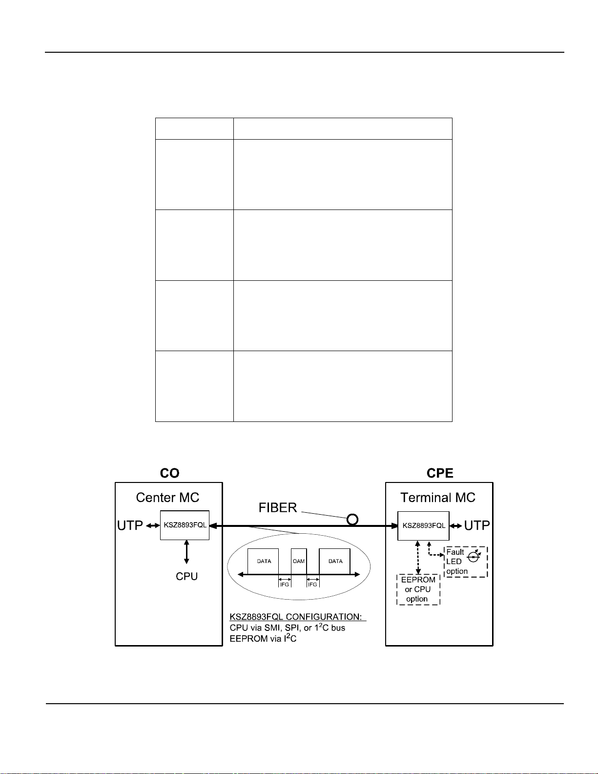
Micrel, Inc. KSZ8893FQL
Media Converter Modes
TS-1000 Media Converter (MC) modes are selected and configured using hardware pins: MCHS and MCCS. The MC
modes are summarized in the following table and are also shown in the Pin Description and I/O Assignment section.
(MCHS, MCCS) Description
Normal 3 port switch mode (3 MAC + 2 PHY)
MC mode is disabled.
(0, 0)
(0, 1)
(1, 0)
(1, 1)
Port 1 is either Fiber or UTP.
Port 2 is UTP.
Port 3 (MII) is enabled.
Center MC mode (3 MAC + 2 PHY)
MC mode is enabled.
Port 1 is Fiber & has Center MC enabled.
Port 2 is UTP.
Port 3 (MII) is enabled.
Terminal MC mode (2 MAC + 2 PHY)
MC mode is enabled.
Port 1 is Fiber & has Terminal MC enabled.
Port 2 is UTP.
Port 3 (MII) is disabled.
Terminal MC mode (3 MAC + 2 PHY)
MC mode is enabled.
Port 1 is Fiber & has Terminal MC enabled.
Port 2 is UTP.
Port 3 (MII) is enabled.
Table 1. TS-1000 Media Converter Mode Selection
The following figure shows two KSZ8893FQLs connected in a typical center MC to terminal MC application.
Figure 2. Typical TS-1000 Media Converter Application
October 2007
24
M9999-101607-1.3
Page 25
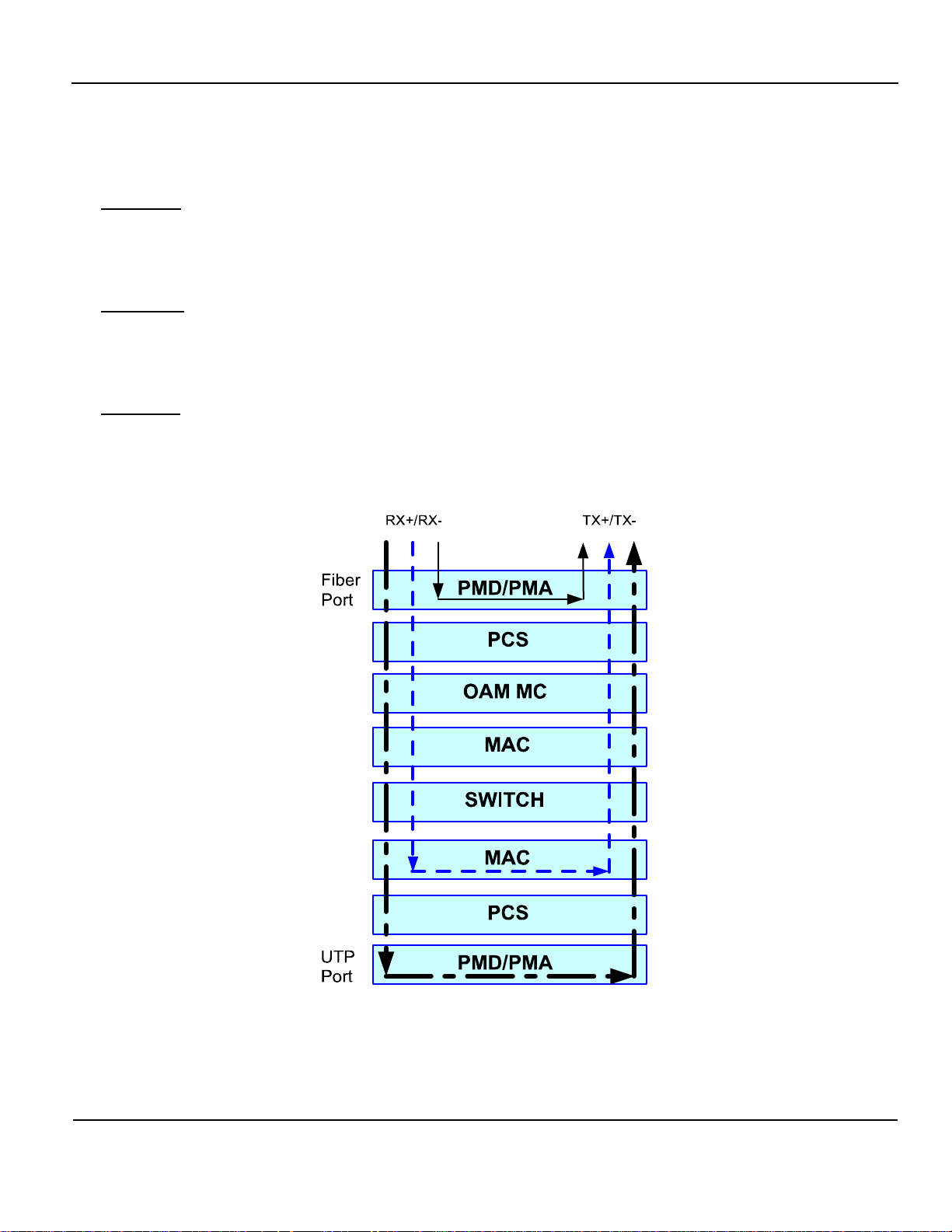
Micrel, Inc. KSZ8893FQL
MC Loop Back Operation
TS-1000 MC loop back operation is initiated and enabled by the center MC. The terminal MC provides the loop back
path to return the loop back packet back to the center MC. The KSZ8893FQL in terminal MC mode provides three loop
back path options:
Port 1 OPT
Port 2 MAC
Port 2 UTP
• Receive loop back packet from center MC at RXP1/RXM1 input pins of port 1 (fiber).
• Turn around loop back packet at PMD/PMA of port 1 (fiber).
• Transmit loop back packet back to center MC from TXP1/TXM1 output pins of port 1 (fiber).
• Receive loop back packet from center MC at RXP1/RXM1 input pins of port 1 (fiber).
• Turn around loop back packet at MAC of port 2 (copper).
• Transmit loop back packet back to center MC from TXP1/TXM1 output pins of port 1 (fiber).
• Receive loop back packet from center MC at RXP1/RXM1 input pins of port 1 (fiber).
• Turn around loop back packet at PMD/PMA of port 2 (copper).
• Transmit loop back packet back to center MC from TXP1/TXM1 output pins of port 1 (fiber).
October 2007
Figure 3. KSZ8893FQL MC Loop Back Paths
25
M9999-101607-1.3
Page 26

Micrel, Inc. KSZ8893FQL
Dedicated TS-1000 Registers & Pins
The KSZ8893FQL provides 32 dedicated registers to support TS-1000 OAM communication in center MC and terminal
MC modes. The TS-1000 MC registers are located at 64 to 95 (0x40 to 0x5F), and provide the following functions:
• PHY address configuration
• Center MC and Terminal MC configuration
• OAM frame selection and execution
• MC loop back setup
• MC loop back counters for CRC error, timeout, good packet
• Remote command access
• Counters for valid MC packet transmitted and received
• MC (local) - status, vendor code, and model number
• Link Partner (remote) - status, vendor code, and model number
The following table lists the dedicated KSZ8893FQL pins used in center MC and terminal MC modes.
Pin Signal Name Type Description
9 MCHS Ipd
10 MCCS Ipd
11 PDD# Ipu
17 P1FST Opu
18 P1CRCD Ipd
19 P1LPBM Ipd
34 ML_EN Ipd
35 DIAGF Ipd
Selects center MC and terminal MC modes. See “Media Converter
Modes” subsection for details.
Power Down Detect – Use by terminal MC to detect a power-down
condition or indicate a failure has occurred.
1 = Normal operation
0 = Power down detected
After detecting a high-to-low transition on this pin, the KSZ8893FQL then
sends out an “Indicate Terminal MC Condition” OAM frame with the S0
status bit set to ‘1’ to inform the center MC that a power down condition
or failure has occurred on the terminal MC side.
If this pin is implemented, PWRDN (pin 36) needs to be de-asserted
(pulled up).
Drives low to indicate fault conditions (far-end fault detected, link
partner’s fiber or UTP port down), or MC loop back mode. This pin has
8mA drive and can directly drive a LED.
Used by terminal MC for MC loop back – strap-in pin to select:
1 = Drop OAM frames and Ethernet frames with the following errors –
CRC, undersize, oversize. Loop back Ethernet frames with only good
CRC and valid length.
0 = Drop OAM frames only. Loop back all Ethernet frames including
those with errors.
Used by terminal MC for MC loop back – strap-in pin to select:
1 = Perform MC loop back at PHY of port 1
0 = Perform MC loop back at MAC of port 2
See also register 11 (0x0B) bits[3:2].
Used by terminal MC for Missing Link Indication – strap-in pin to select:
1 = Enable Missing Link feature
0 = Disable Missing Link feature
Used by terminal MC for Diagnostic status
1 = Diagnostic fail
0 = Diagnostic normal
After detecting a change of state on this pin, the KSZ8893FQL sends out
an “Indicate Terminal MC Condition” OAM frame with the S3 status bit
set to the state of this pin to inform the center MC that a diagnostic status
change has occurred on the terminal MC side.
October 2007
Table 2. Dedicated TS-1000 Pins
26
M9999-101607-1.3
Page 27

Micrel, Inc. KSZ8893FQL
10Base-FL Operation
10Base-FL operation is supported on port 1 of the KSZ8893FQL. It conforms to clause 15 and 18 of the IEEE802.3
Standard for 10Base-FL fiber operation. Refer to the Standard for details.
In a typical application, the KSZ8893FQL provides media conversion from 10Base-FL fiber on port 1 to 10Base-T
copper on port 2. Alternatively, port 2 can be substituted with port 3 to directly connect to an external MAC.
Physical Interface
For 10Base-FL operation, port 1 interfaces with an external fiber module to drive 850nm fiber optic links. The interface
connections between the KSZ8893FQL and fiber module are single-ended (common mode). 10Base-FL signal
transmission and reception are done on TXM1 (pin 49) and RXM1 (pin 46), respectively. Refer to Micrel reference
schematic for recommended interface circuit and termination.
Enabling 10Base-FL Mode
To enable 10Base-FL mode, tie FXSD1 (pin 44) high to +3.3V and MUX2 (pin 41) low-to-ground. Port 1 should also be
configured with auto-negotiation disabled, forced to 10Mbps for the speed, and set to either half or full duplex.
Optionally, flow control can be enabled to send out PAUSE frames in full duplex mode.
The 10Base-FL settings use the same strapping pins, MIIM registers and port registers as 10Base-T copper. These
settings are summarized in the following table.
Strapping Pin (#) MIIM Register #, Bit[#] Port Register #, Bit[#]
10Base-FL Settings
Auto-Negotiation (disable only) P1ANEN (30) Reg. 0, Bit[12] Reg. 28, Bit[7]
Speed (10Mbps only) P1SPD (31) Reg. 0, Bit[13] Reg. 28, Bit[6]
Duplex (half or full) P1DPX (32) Reg. 0, Bit[8] Reg. 28, Bit[5]
Forced Flow Control (option) P1FFC (33) --- Reg. 18, Bit[4]
Table 3. 10Base-FL Configuration
100Base-SX Operation
100Base-SX operation is supported on port 1 of the KSZ8893FQL. It conforms to the TIA/EIA-785 Standard for
100Base-SX fiber operation. Refer to the Standard for details.
In a typical application, the KSZ8893FQL provides media conversion from 100Base-SX fiber on port 1 to 100Base-TX
copper on port 2. Alternatively, port 2 can be substituted with port 3 to directly connect to an external MAC.
Physical Interface
For 100Base-SX operation, port 1 interfaces with an external fiber module to drive 850nm fiber optic links. The interface
connections between the KSZ8893FQL and fiber module are single-ended (common mode). 100Base-SX signal
transmission and reception are done on TXM1 (pin 49) and RXM1 (pin 46), respectively. Refer to Micrel’s reference
schematic for recommended interface circuit and termination.
Enabling 100Base-SX Mode
To enable 100Base-SX mode, tie FXSD1 (pin 44) high to +3.3V and MUX2 (pin 41) low-to-ground. Port 1 should also
be configured with auto-negotiation disabled, forced to 100Mbps for the speed, and set to either half or full duplex.
Optionally, flow control can be enabled to send out PAUSE frames in full duplex mode.
The 100Base-SX settings use the same strapping pins, MIIM registers and port registers as 100Base-TX copper. These
settings are summarized in the following table.
October 2007
27
M9999-101607-1.3
Page 28

Micrel, Inc. KSZ8893FQL
Strapping Pin (#) MIIM Register #, Bit[#] Port Register #, Bit[#]
100Base-SX Settings
Auto-Negotiation (disable only) P1ANEN (30) Reg. 0, Bit[12] Reg. 28, Bit[7]
Speed (100Mbps only) P1SPD (31) Reg. 0, Bit[13] Reg. 28, Bit[6]
Duplex (half or full) P1DPX (32) Reg. 0, Bit[8] Reg. 28, Bit[5]
Forced Flow Control (option) P1FFC (33) --- Reg. 18, Bit[4]
Table 4. 100Base-SX Configuration
Functional Overview: Physical Layer Transceiver
100Base-TX Transmit
The 100Base-TX transmit function performs parallel-to-serial conversion, 4B/5B coding, scrambling, NRZ-to-NRZI
conversion, and MLT3 encoding and transmission.
The circuitry starts with a parallel-to-serial conversion, which converts the MII data from the MAC into a 125MHz serial
bit stream. The data and control stream is then converted into 4B/5B coding, followed by a scrambler. The serialized
data is further converted from NRZ-to-NRZI format, and then transmitted in MLT3 current output. The output current is
set by an external 1% 3.01KΩ resistor for the 1:1 transformer ratio.
The output signal has a typical rise/fall time of 4ns and complies with the ANSI TP-PMD standard regarding amplitude
balance, overshoot, and timing jitter. The wave-shaped 10Base-T output is also incorporated into the 100Base-TX
transmitter.
100Base-TX Receive
The 100Base-TX receiver function performs adaptive equalization, DC restoration, MLT3-to-NRZI conversion, data and
clock recovery, NRZI-to-NRZ conversion, de-scrambling, 4B/5B decoding, and serial-to-parallel conversion.
The receiving side starts with the equalization filter to compensate for inter-symbol interference (ISI) over the twisted
pair cable. Since the amplitude loss and phase distortion is a function of the cable length, the equalizer must adjust its
characteristics to optimize performance. In this design, the variable equalizer makes an initial estimation based on
comparisons of incoming signal strength against some known cable characteristics, and then tunes itself for
optimization. This is an ongoing process and self-adjusts against environmental changes such as temperature
variations.
Next, the equalized signal goes through a DC restoration and data conversion block. The DC restoration circuit is used
to compensate for the effect of baseline wander and to improve the dynamic range. The differential data conversion
circuit converts the MLT3 format back to NRZI. The slicing threshold is also adaptive.
The clock recovery circuit extracts the 125MHz clock from the edges of the NRZI signal. This recovered clock is then
used to convert the NRZI signal into the NRZ format. This signal is sent through the de-scrambler followed by the 4B/5B
decoder. Finally, the NRZ serial data is converted to the MII format and provided as the input data to the MAC.
PLL Clock Synthesizer
The KSZ8893FQL generates 125MHz, 31.25MHz, 25MHz, and 10MHz clocks for system timing. Internal clocks are
generated from an external 25MHz crystal or oscillator. In RMII mode, these internal clocks are generated from an
external 50MHz oscillator or system clock.
Scrambler/De-scrambler (100Base-TX Only)
The purpose of the scrambler is to spread the power spectrum of the signal to reduce electromagnetic interference
(EMI) and baseline wander. Transmitted data is scrambled through the use of an 11-bit wide linear feedback shift
register (LFSR). The scrambler generates a 2047-bit non-repetitive sequence, and the receiver then de-scrambles the
incoming data stream using the same sequence as at the transmitter.
October 2007
28
M9999-101607-1.3
Page 29

Micrel, Inc. KSZ8893FQL
100Base-FX Operation
100Base-FX operation is similar to 100Base-TX operation with the differences being that the scrambler/de-scrambler
and MLT3 encoder/decoder are bypassed on transmission and reception. In addition, auto-negotiation is bypassed and
auto MDI/MDI-X is disabled.
100Base-FX Signal Detection
In 100Base-FX operation, FXSD1 (fiber signal detect), input pin 44, is usually connected to the fiber transceiver SD
(signal detect) output pin. 100Base-FX mode is activated when the FXSD1 input pin is greater than 1V. When FXSD1 is
between 1V and 1.8V, no fiber signal is detected and a far-end fault (FEF) is generated. When FXSD1 is over 2.2V, the
fiber signal is detected.
Alternatively, the designer may choose not to implement the FEF feature. In this case, the FXSD1 input pin is tied high
to force 100Base-FX mode.
100Base-FX signal detection is summarized in the following table:
FXSD1 Input Voltage Mode
Less than 0.2V TX mode
Greater than 1V, but less than 1.8V FX mode
No signal detected
Far-end fault generated
Greater than 2.2V FX mode
Signal detected
Table 5. FX and TX Mode Selection
To ensure proper operation, a resistive voltage divider is recommended to adjust the fiber transceiver SD output voltage
swing to match the FXSD1 pin’s input voltage threshold.
100Base-FX Far-End Fault
A far-end fault (FEF) occurs when the signal detection is logically false on the receive side of the fiber transceiver. The
KSZ8893FQL detects a FEF when its FXSD1 input is between 1V and 1.8V. When a FEF is detected, the
KSZ8893FQL signals its fiber link partner that a FEF has occurred by sending 84 1’s followed by a zero in the idle
period between frames.
By default, FEF is enabled. FEF can be disabled through register setting.
10Base-T Transmit
The 10Base-T driver is incorporated with the 100Base-TX driver to allow for transmission using the same magnetics.
They are internally wave-shaped and pre-emphasized into outputs with typical 2.3V amplitude. The harmonic contents
are at least 27dB below the fundamental frequency when driven by an all-ones Manchester-encoded signal.
10Base-T Receive
On the receive side, input buffers and level detecting squelch circuits are employed. A differential input receiver circuit
and a phase-locked loop (PLL) perform the decoding function. The Manchester-encoded data stream is separated into
clock signal and NRZ data. A squelch circuit rejects signals with levels less than 400mV or with short pulse widths to
prevent noise at the RXP-or-RXM input from falsely triggering the decoder. When the input exceeds the squelch limit,
the PLL locks onto the incoming signal and the KSZ8893FQL decodes a data frame. The receiver clock is maintained
active during idle periods in between data reception.
Fiber LED Driver
The device provides a current mode fiber LED driver. The edge enhanced current mode does not require any output
wave shaping. The drive current of the fiber LED driver is programmable thru register 138 (0x8A) bit[7:6]. The
programmable current values are as follow:
October 2007
29
M9999-101607-1.3
Page 30

Micrel, Inc. KSZ8893FQL
Reg. 138 (0x8A) bit[7:6] Current Value
00 60mA
01 80mA
10 90mA
11 40mA
Table 6. Programmable Current Values for Fiber LED Driver
Post Amplifier
The KSZ8893FQL also includes a post amplifier. The post amplifier is intended for interfacing the output of the preamplifier of the PIN diode module. The minimum sensitivity of the post amplifier is 2.5mV
rms
.
Power Management
The KSZ8893FQL features a per-port power down mode. To save power, a PHY port that is not in use can be powered
down via port control register, or via MIIM PHY register.
In addition, there is a full chip power down mode. When activated, the entire chip is powered down.
MDI/MDI-X Auto Crossover
To eliminate the need for crossover cables between similar devices, the KSZ8893FQL offers HP Auto MDI/MDI-X and
Micrel Auto MDI/MDI-X crossover. HP Auto MDI/MDI-X is the default.
The auto-sense function detects remote transmit and receive pairs and correctly assigns transmit and receive pairs for
the KSZ8893FQL device. This feature is extremely useful when end users are unaware of cable types, and also, saves
on an additional uplink configuration connection. The auto-crossover feature can be disabled through the port control
registers, or MIIM PHY registers.
The IEEE 802.3u standard MDI and MDI-X definitions are:
MDI MDI-X
RJ-45 Pins Signals RJ-45 Pins Signals
1 TD+ 1 RD+
2 TD- 2 RD-
3 RD+ 3 TD+
6 RD- 6 TD-
Table 7. MDI/MDI-X Pin Definitions
Straight Cable
A straight cable connects an MDI device to an MDI-X device, or an MDI-X device to an MDI device. The following
diagram depicts a typical straight cable connection between a NIC card (MDI) and a switch, or hub (MDI-X).
October 2007
30
M9999-101607-1.3
Page 31

Micrel, Inc. KSZ8893FQL
10/100 Ethernet
Media Dependent Interface
10/100 Ethernet
Media Dependent Interface
Receive Pair
Modular Connector
(RJ-45)
NIC
1
2
3
4
5
6
7
8
Straight
Cable
1
Receive PairTransmit Pair
2
3
4
Transmit Pair
5
6
7
8
Modular Connector
(RJ-45)
HUB
(Repeater or Switch)
Figure 4. Typical Straight Cable Connection
Crossover Cable
A crossover cable connects an MDI device to another MDI device, or an MDI-X device to another MDI-X device. The
following diagram shows a typical crossover cable connection between two switches or hubs (two MDI-X devices).
10/100 Ethernet
Media Dependent Interface
1
Receive Pair Receive Pair
2
3
4
Transmit Pair
5
6
7
8
Modular Connector (RJ-45)
HUB
(Repeater or Switch)
Crossover
Cable
10/100 Ethernet
Media Dependent Interface
1
2
3
4
Transmit Pair
5
6
7
8
Modular Connector (RJ-45)
HUB
(Repeater or Switch)
Figure 5. Typical Crossover Cable Connection
October 2007
31
M9999-101607-1.3
Page 32

Micrel, Inc. KSZ8893FQL
Auto-Negotiation
The KSZ8893FQL conforms to the auto-negotiation protocol, as defined in Clause 28 of the IEEE 802.3u specification.
Auto-negotiation allows unshielded twisted pair (UTP) link partners to select the best common mode of operation. In
auto-negotiation, link partners advertise their capabilities across the link to each other. If auto-negotiation is not
supported or the KSZ8893FQL link partner is forced to bypass auto-negotiation, then the KSZ8893FQL sets its
operating mode by observing the signal at its receiver. This is known as parallel detection, and allows the KSZ8893FQL
to establish link by listening for a fixed signal protocol in the absence of auto-negotiation advertisement protocol.
The link up process is shown in the following flow diagram.
October 2007
Figure 6. Auto-Negotiation and Parallel Operation
32
M9999-101607-1.3
Page 33

Micrel, Inc. KSZ8893FQL
LinkMD Cable Diagnostics
The LinkMD feature utilizes time domain reflectometry (TDR) to analyze the cabling plant for common cabling problems
such as open circuits, short circuits and impedance mismatches.
LinkMD works by sending a pulse of known amplitude and duration down the MDI and MDI-X pairs and then analyzes
the shape of the reflected signal. Timing the pulse duration gives an indication of the distance to the cabling fault with
maximum distance of 200m and accuracy of +/- 2m. Internal circuitry displays the TDR information in a user-readable
digital format.
Note: Cable diagnostics are only valid for copper connections and do not support fiber optic operation.
Access
LinkMD is initiated by accessing registers {26,27} and {42,43}, the LinkMD Control/Status registers, for ports 1 and 2,
respectively; and in conjunction with registers 29 and 45, Port Control Register 13, for ports 1 and 2, respectively.
Alternatively, the MIIM PHY registers 0 and 29 can be used for LinkMD access.
Usage
The following is a sample procedure for using LinkMD with registers {26,27,29} on port 1.
1. Disable auto MDI/MDI-X by writing a ‘1’ to register 29, bit [2] to enable manual control over the differential pair
used to transmit the LinkMD pulse.
2. Start cable diagnostic test by writing a ‘1’ to register 26, bit [4]. This enable bit is self-clearing.
3. Wait (poll) for register 26, bit [4] to return a ‘0’; indicating cable diagnostic test is completed.
4. Read cable diagnostic test results in register 26, bits [6:5]. The results are as follows:
00 = normal condition (valid test)
01 = open condition detected in cable (valid test)
10 = short condition detected in cable (valid test)
11 = cable diagnostic test failed (invalid test)
The ‘11’ case, invalid test, occurs when the KSZ8893FQL is unable to shut down the link partner. In this
instance, the test is not run, since it would be impossible for the KSZ8893FQL to determine if the detected
signal is a reflection of the signal generated or a signal from another source.
5. Get distance to fault by concatenating register 26, bit [0] and register 27, bits [7:0], and multiplying the result by
a constant of 0.4. The distance to the cable fault can be determined by the following formula:
D (distance to cable fault) = 0.4 x {(register 26, bit [0]),(register 27, bits [7:0])}
D (distance to cable fault) is expressed in meters.
Concatenated value of registers 26 and 27 is converted to decimal before multiplying by 0.4.
The constant (0.4) may be calibrated for different cabling conditions, including cables with a velocity of
propagation that varies significantly from the norm.
For port 2 and for the MIIM PHY registers, LinkMD usage is similar.
October 2007
33
M9999-101607-1.3
Page 34

Micrel, Inc. KSZ8893FQL
Functional Overview: MAC and Switch
Address Lookup
The internal lookup table stores MAC addresses and their associated information. It contains a 1K unicast address
table plus switching information.
The KSZ8893FQL is guaranteed to learn 1K addresses and distinguishes itself from hash-based look-up tables, which
depending upon the operating environment and probabilities, may not guarantee the absolute number of addresses it
can learn.
Learning
The internal look-up engine updates its table with a new entry if the following conditions are met:
1. The received packet's Source Address (SA) does not exist in the lookup table.
2. The received packet is good; the packet has no receiving errors, and is of legal length.
The lookup engine inserts the qualified SA into the table, along with the port number and time stamp. If the table is full,
then the last entry of the table is deleted to make room for the new entry.
Migration
The internal look-up engine also monitors whether a station has moved. If a station has moved, it will update the table
accordingly. Migration occurs when the following conditions are met:
1. The received packet's SA is in the table but the associated source port information is different.
2. The received packet is good; the packet has no receiving errors, and is of legal length.
The lookup engine will update the existing record in the table with the new source port information.
Aging
The look-up engine updates the time stamp information of a record whenever the corresponding SA appears. The time
stamp is used in the aging process. If a record is not updated for a period of time, the look-up engine removes the
record from the table. The look-up engine constantly performs the aging process and will continuously remove aging
records. The aging period is about 200 seconds. This feature can be enabled or disabled through register 3 (0x03) bit
[2].
Forwarding
The KSZ8893FQL forwards packets using the algorithm that is depicted in the following flowcharts. Figure 7 shows
stage one of the forwarding algorithm where the search engine looks up the VLAN ID, static table, and dynamic table
for the destination address, and comes up with “port to forward 1” (PTF1). PTF1 is then further modified by spanning
tree, IGMP snooping, port mirroring, and port VLAN processes to come up with “port-to-forward 2” (PTF2), as shown in
Figure 8. The packet is sent to PTF2.
October 2007
34
M9999-101607-1.3
Page 35

Micrel, Inc. KSZ8893FQL
October 2007
Figure 7. Destination Address Lookup Flow Chart, Stage 1
35
M9999-101607-1.3
Page 36

Micrel, Inc. KSZ8893FQL
Figure 8. Destination Address Resolution Flow Chart, Stage 2
The KSZ8893FQL will not forward the following packets:
1. Error packets
These include framing errors, Frame Check Sequence (FCS) errors, alignment errors, and illegally sized packet
errors.
2. IEEE802.3x PAUSE frames
KSZ8893FQL intercepts these packets and performs full duplex flow control accordingly.
3. "Local" packets
Based on destination address (DA) lookup. If the destination port from the look-up table matches the port from
which the packet originated, the packet is defined as "local."
October 2007
36
M9999-101607-1.3
Page 37

Micrel, Inc. KSZ8893FQL
Switching Engine
The KSZ8893FQL features a high-performance switching engine that moves data to and from the MACs’ packet
buffers. It operates in store and forward mode, while the efficient switching mechanism reduces overall latency.
The switching engine has a 32kB internal frame buffer. This buffer pool is shared between all three ports. There are a
total of 256 buffers available. Each buffer is sized at 128 bytes.
MAC Operation
The KSZ8893FQL strictly abides by IEEE 802.3 standards to maximize compatibility.
Inter Packet Gap (IPG)
If a frame is successfully transmitted, the 96 bits time IPG is measured between the two consecutive MTXEN. If the
current packet is experiencing collision, the 96 bits time IPG is measured from MCRS and the next MTXEN.
Back-Off Algorithm
The KSZ8893FQL implements the IEEE 802.3 standard for the binary exponential back-off algorithm, and optional
"aggressive mode" back-off. After 16 collisions, the packet is optionally dropped depending upon the switch
configuration for register 4 (0x04) bit [3].
Late Collision
If a transmit packet experiences collisions after 512 bit times of the transmission, the packet is dropped.
Illegal Frames
The KSZ8893FQL discards frames less than 64 bytes, and can be programmed to accept frames up to 1518 bytes,
1536 bytes or 1916 bytes. These maximum frame size settings are programmed in register 4 (0x04). Since the
KSZ8893FQL supports VLAN tags, the maximum sizing is adjusted when these tags are present.
Full Duplex Flow Control
The KSZ8893FQL supports standard IEEE 802.3x flow control frames on both the transmit and the receive sides.
On the receive side, if the KSZ8893FQL receives a pause control frame, then the KSZ8893FQL will not transmit the
next normal frame until the timer, specified in the pause control frame, expires. If another pause frame is received
before the current timer expires, then the timer will be updated with the new value in the second pause frame. During
this period (while it is flow controlled), only flow control packets from the KSZ8893FQL are transmitted.
On the transmit side, the KSZ8893FQL has intelligent and efficient ways to determine when to invoke flow control. The
flow control is based upon availability of the system resources, including available buffers, available transmit queues
and available receive queues.
The KSZ8893FQL will flow control a port that has just received a packet if the destination port resource is busy. The
KSZ8893FQL issues a flow control frame (XOFF), containing the maximum pause time defined by the IEEE 802.3x
standard. Once the resource is freed up, the KSZ8893FQL then sends out the other flow control frame (XON) with zero
pause time to turn off the flow control (turn on transmission to the port). A hysteresis feature is provided to prevent the
flow control mechanism from being constantly activated and deactivated.
The KSZ8893FQL flow controls all ports if the receive queue becomes full.
Half-Duplex Backpressure
A half-duplex backpressure option (not in IEEE 802.3 standards) is also provided. The activation and deactivation
conditions are the same as full duplex flow control. If backpressure is required, then the KSZ8893FQL sends preambles
to defer the other stations' transmission (carrier sense deference).
To avoid jabber and excessive deference (as defined in the 802.3 standard), after a certain time, the KSZ8893FQL
discontinues the carrier sense and then raises it again quickly. This short silent time (no carrier sense) prevents other
stations from sending out packets thereby keeping other stations in a ‘carrier sense’ deferred state. If the port has
packets to send during a backpressure situation, then the carrier sense type backpressure is interrupted and those
packets are transmitted instead. If there are no additional packets to send, carrier sense type backpressure is
reactivated again until switch resources free up. If a collision occurs, the binary exponential back-off algorithm is
October 2007
37
M9999-101607-1.3
Page 38

Micrel, Inc. KSZ8893FQL
skipped and carrier sense is generated immediately, thereby reducing the chance of further collisions and carrier sense
is maintained to prevent packet reception.
To ensure no packet loss in 10 Base-T or 100 Base-TX half duplex modes, the user must enable the following:
1. Aggressive back-off (register 3 (0x03), bit [0])
2. No excessive collision drop (register 4 (0x04), bit [3])
Note: These bits are not set as defaults, as this is not the IEEE standard.
Broadcast Storm Protection
The KSZ8893FQL has an intelligent option to protect the switch system from receiving too many broadcast packets. As
the broadcast packets are forwarded to all ports except the source port, an excessive number of switch resources
(bandwidth and available space in transmit queues) may be utilized. The KSZ8893FQL has the option to include
“multicast packets” for storm control. The broadcast storm rate parameters are programmed globally, and can be
enabled or disabled on a per port basis. The rate is based upon a 67ms interval for 100BT and a 500ms interval for
10BT. At the beginning of each interval, the counter is cleared to zero, and the rate limit mechanism starts to count the
number of bytes during the interval. The rate definition is described in register 6 (0x06) and 7 (0x07). The default setting
is 0x63 (99 decimal). This is equal to a rate of 1%, calculated as follows:
148,800 frames/sec * 67ms/interval * 1% = 99 frames/interval (approx.) = 0x63
Note: 148,800 frames/sec is based on 64-byte block of packets in 100Base-TX with 12 bytes of IPG and 8 bytes of
preamble between two packets.
MII Interface Operation
The Media Independent Interface (MII) is specified in Clause 22 of the IEEE 802.3u Standard. It provides a common
interface between physical layer and MAC layer devices. The MII provided by the KSZ8893FQL is connected to the
device’s third MAC. The interface contains two distinct groups of signals: one for transmission and the other for
reception. The following table describes the signals used by the MII bus.
PHY-Mode Connections MAC-Mode Connections
External MAC
Controller Signals
MTXEN SMTXEN Transmit enable MTXEN SMRXDV
MTXER SMTXER Transmit error MTXER (not used)
MTXD3 SMTXD[3] Transmit data bit 3 MTXD3 SMRXD[3]
MTXD2 SMTXD[2] Transmit data bit 2 MTXD2 SMRXD[2]
MTXD1 SMTXD[1] Transmit data bit 1 MTXD1 SMRXD[1]
MTXD0 SMTXD[0] Transmit data bit 0 MTXD0 SMRXD[0]
MTXC SMTXC Transmit clock MTXC SMRXC
MCOL SCOL Collision detection MCOL SCOL
MCRS SCRS Carrier sense MCRS SCRS
MRXDV SMRXDV Receive data valid MRXDV SMTXEN
MRXER (not used) Receive error MRXER SMTXER
MRXD3 SMRXD[3] Receive data bit 3 MRXD3 SMTXD[3]
MRXD2 SMRXD[2] Receive data bit 2 MRXD2 SMTXD[2]
MRXD1 SMRXD[1] Receive data bit 1 MRXD1 SMTXD[1]
MRXD0 SMRXD[0] Receive data bit 0 MRXD0 SMTXD[0]
MRXC SMRXC Receive clock MRXC SMTXC
KSZ8893FQL
PHY Signals
Pin
Descriptions
Table 8. MII Signals
External
PHY Signals
KSZ8893FQL
MAC Signals
October 2007
38
M9999-101607-1.3
Page 39

Micrel, Inc. KSZ8893FQL
The MII operates in either PHY mode or MAC mode. The data interface is a nibble wide and runs at one-quarter the
network bit rate (not encoded). Additional signals on the transmit side indicate when data is valid or when an error has
occurred during transmission. Similarly, the receive side has signals that convey when the data is valid and without
physical layer errors. For half-duplex operation, the SCOL signal indicates if a collision has occurred during
transmission.
The KSZ8893FQL does not provide the MRXER signal for PHY mode operation and the MTXER signal for MAC mode
operation. Normally, MRXER indicates a receive error coming from the physical layer device and MTXER indicates a
transmit error from the MAC device. Since the switch filters error frames, these MII error signals are not used by the
KSZ8893FQL. So, for PHY mode operation, if the device interfacing with the KSZ8893FQL has an MRXER input pin, it
needs to be tied low. And, for MAC mode operation, if the device interfacing with the KSZ8893FQL has an MTXER
input pin, it also needs to be tied low.
RMII Interface Operation
The Reduced Media Independent Interface (RMII) specifies a low pin count Media Independent Interface (MII). RMII
provides a common interface between physical layer and MAC layer devices, and has the following key characteristics:
1. Supports 10Mbps and 100Mbps data rates.
2. Uses a single 50 MHz clock reference (provided externally).
3. Provides independent 2-bit wide (di-bit) transmit and receive data paths.
4. Contains two distinct groups of signals: one for transmission and the other for reception
The RMII provided by the KSZ8893FQL is connected to the device’s third MAC. It complies with the RMII Specification.
The following table describes the signals used by the RMII bus. Refer to RMII Specification for full detail on the signal
description.
RMII
Signal Name
REF_CLK Input
CRS_DV Output Input
RXD1 Output Input Receive data bit 1 SMRXD[1] (output)
RXD0 Output Input Receive data bit 0 SMRXD[0] (output)
TX_EN Input Output Transmit enable SMTXEN (input)
TXD1 Input Output Transmit data bit 1 SMTXD[1] (input)
TXD0 Input Output Transmit data bit 0 SMTXD[0] (input)
RX_ER Output
--- --- --- ---
Direction
(with respect
to the PHY)
Direction
(with respect
to the MAC)
Input or
Output
Input
(not required)
Table 9. RMII Signal Description
RMII
Signal Description
Synchronous 50 MHz clock
reference for receive, transmit
and control interface
Carrier sense/
Receive data valid
Receive error (not used)
KSZ8893FQL RMII
Signal (direction)
REFCLK (input)
SMRXDV (output)
SMTXER* (input)
* Connects to RX_ER
signal of RMII PHY device
October 2007
39
M9999-101607-1.3
Page 40

Micrel, Inc. KSZ8893FQL
The KSZ8893FQL filters error frames, and thus does not implement the RX_ER output signal. To detect error frames
from RMII PHY devices, the SMTXER input signal of the KSZ8893FQL is connected to the RXER output signal of the
RMII PHY device.
Collision detection is implemented in accordance with the RMII Specification.
In RMII mode, tie MII signals, SMTXD[3:2] and SMTXER, to ground if they are not used.
The KSZ8893FQL RMII can interface with RMII PHY and RMII MAC devices. The latter allows two KSZ8893FQL
devices to be connected back-to-back. The following table shows the KSZ8893FQL RMII pin connections with an
external RMII PHY and an external RMII MAC, such as another KSZ8893FQL device.
KSZ8893FQL
PHY-MAC Connections
External
PHY Signals
REF_CLK REFCLK Reference Clock REFCLK REF_CLK
CRS_DV SMRXDV
RXD1 SMRXD[1]
RXD0 SMRXD[0]
TX_EN SMTXEN Transmit enable SMTXEN TX_EN
TXD1 SMTXD[1] Transmit data bit 1 SMTXD[1] TXD1
TXD0 SMTXD[0] Transmit data bit 0 SMTXD[0] TXD0
RX_ER SMTXER Receive error (not used) (not used)
KSZ8893FQL
MAC Signals
Pin
Descriptions
Carrier sense/
Receive data valid
Receive data bit 1
Receive data bit 0
Table 10. RMII Signal Connections
KSZ8893FQL
MAC Signals
SMRXDV CRS_DV
SMRXD[1] RXD1
SMRXD[0] RXD0
KSZ8893FQL
MAC-MAC Connections
External
MAC Signals
SNI (7-Wire) Operation
The serial network interface (SNI) or 7-wire is compatible with some controllers used for network layer protocol
processing. In SNI mode, the KSZ8893FQL acts like a PHY and the external controller functions as the MAC. The
KSZ8893FQL can interface directly with external controllers using the 7-wire interface. These signals are divided into
two groups, one for transmission and the other for reception. The signals involved are described in the following table.
Pin Descriptions External MAC
Controller Signals
Transmit enable TXEN SMTXEN
Serial transmit data TXD SMTXD[0]
Transmit clock TXC SMTXC
Collision detection COL SCOL
Carrier sense CRS SMRXDV
Serial receive data RXD SMRXD[0]
Receive clock RXC SMRXC
KSZ8893FQL
PHY Signals
Table 11. SNI Signals
The SNI interface is a bit wide data interface and therefore, runs at the network bit rate (not encoded). An additional
signal on the transmit side indicates when data is valid. Similarly, the receive side has an indicator that conveys when
the data is valid.
For half duplex operation, the SCOL signal is used to indicate that a collision has occurred during transmission.
October 2007
40
M9999-101607-1.3
Page 41

Micrel, Inc. KSZ8893FQL
MII Management (MIIM) Interface
The KSZ8893FQL supports the IEEE 802.3 MII Management Interface, also known as the Management Data
Input/Output (MDIO) Interface. This interface allows upper-layer devices to monitor and control the states of the
KSZ8893FQL. An external device with MDC/MDIO capability is used to read the PHY status or configure the PHY
settings. Further details on the MIIM interface can be found in Clause 22.2.4.5 of the IEEE 802.3u Specification.
The MIIM interface consists of the following:
• A physical connection that incorporates the data line (MDIO) and the clock line (MDC).
• A specific protocol that operates across the aforementioned physical connection that allows an external
controller to communicate with the KSZ8893FQL device.
• Access to a set of eight 16-bit registers, consisting of six standard MIIM registers [0:5] and two custom MIIM
registers [29, 31].
The MIIM Interface can operate up to a maximum clock speed of 5 MHz.
The following table depicts the MII Management Interface frame format.
Preamble
Read
Write
32 1’s 01 10 AAAAA RRRRR Z0 DDDDDDDD_DDDDDDDD Z
32 1’s 01 01 AAAAA RRRRR 10 DDDDDDDD_DDDDDDDD Z
Start of
Frame
Read/Write
OP Code
Table 12. MII Management Interface Frame Format
PHY
Address
Bits [4:0]
REG
Address
Bits [4:0]
TA Data
Idle
Bits [15:0]
Serial Management Interface (SMI)
The SMI is the KSZ8893FQL non-standard MIIM interface that provides access to all KSZ8893FQL configuration
registers. This interface allows an external device to completely monitor and control the states of the KSZ8893FQL.
The SMI interface consists of the following:
• A physical connection that incorporates the data line (MDIO) and the clock line (MDC).
• A specific protocol that operates across the aforementioned physical connection that allows an external
controller to communicate with the KSZ8893FQL device.
• Access to all KSZ8893FQL configuration registers. Register access includes the Global, Port and Advanced
Control Registers 0-141 (0x00 – 0x8D), and indirect access to the standard MIIM registers [0:5] and custom
MIIM registers [29, 31].
The following table depicts the SMI frame format.
Preamble
Read
Write
32 1’s 01 00 1xRRR RRRRR Z0 0000_0000_DDDD_DDDD Z
32 1’s 01 00 0xRRR RRRRR 10 xxxx_xxxx_DDDD_DDDD Z
Start of
Frame
Read/Write
OP Code
PHY
Address
Bits [4:0]
REG
Address
Bits [4:0]
TA Data
Bits [15:0]
Idle
Table 13. Serial Management Interface (SMI) Frame Format
SMI register read access is selected when OP Code is set to “00” and bit 4 of the PHY address is set to ‘1’. SMI register
write access is selected when OP Code is set to “00” and bit 4 of the PHY address is set to ‘0’. PHY address bit[3] is
undefined for SMI register access, and hence, can be set to either ‘0’ or ‘1’ in read/write operations.
To access the KSZ8893FQL registers 0-141 (0x00 – 0x8D), the following applies:
• PHYAD[2:0] and REGAD[4:0] are concatenated to form the 8-bit address; that is, {PHYAD[2:0], REGAD[4:0]} =
bits [7:0] of the 8-bit address.
• Registers are 8 data bits wide.
– For read operation, data bits [15:8] are read back as 0’s.
– For write operation, data bits [15:8] are not defined, and hence can be set to either ‘0’ or ‘1’.
October 2007
41
M9999-101607-1.3
Page 42

Micrel, Inc. KSZ8893FQL
SMI register access is the same as the MIIM register access, except for the register access requirements presented in
this section.
Repeater Mode
The KSZ8893FQL supports repeater mode in 100Base-TX Half Duplex mode. In repeater mode, all ingress packets are
broadcast to the other two ports. MAC address checking and learning are disabled.
Repeater mode is enabled by setting register 6 bit[7] to ‘1’. Prior to setting this bit, all three ports need to be configured
to 100Base-TX Half Duplex mode. Additionally, both PHY ports need to have auto-negotiation disabled.
The latency between the two PHY ports is 270 ns (minimum) and 310 ns (maximum). The 40 ns difference is one clock
skew (one 25 MHz clock period) between reception and transmission. Latency is defined as the time from the first bit of
the Destination Address (DA) entering the ingress port to the first bit of the DA exiting the egress port.
Advanced Switch Functions
Spanning Tree Support
To support spanning tree, port 3 is designated as the processor port.
The other ports (port 1 and port 2), can be configured in one of the five spanning tree states via “transmit enable”,
“receive enable” and “learning disable” register settings in registers 18 and 34 for ports 1 and 2, respectively. The
following table shows the port setting and software actions taken for each of the five spanning tree states.
Disable State Port Setting Software Action
The port should not
forward or receive
any packets.
Learning is
disabled.
Blocking State Port Setting Software Action
Only packets to the
processor are
forwarded.
Learning is
disabled.
Listening State Port Setting Software Action
Only packets to
and from the
processor are
forwarded.
Learning is
disabled.
Learning State Port Setting Software Action
Only packets to
and from the
processor are
forwarded.
Learning is
enabled.
Forwarding State Port Setting Software Action
Packets are
forwarded and
received normally.
Learning is
enabled.
“transmit
enable = 0,
receive
enable = 0,
learning
disable =1”
“transmit
enable = 0,
receive
enable = 0,
learning
disable =1”
“transmit
enable = 0,
receive
enable = 0,
learning
disable =1”
“transmit
enable = 0,
receive
enable = 0,
learning
disable = 0”
“transmit
enable = 1,
receive
enable = 1,
learning
disable = 0”
The processor should not send
specific packets to the processor (packets that match some entries in the “static
MAC table” with “overriding bit” set) and the processor should discard those
packets. Address learning is disabled on the port in this state.
The processor should not send any packets to the port(s) in this state. The
processor should program the “Static MAC table” with the entries that it needs to
receive (for example, BPDU packets). The “overriding” bit should also be set so that
the switch will forward those specific packets to the processor. Address learning is
disabled on the port in this state.
The processor should program the “Static MAC table” with the entries that it needs
to receive (for example, BPDU packets). The “overriding” bit should be set so that
the switch will forward those specific packets to the processor. The processor may
send packets to the port(s) in this state. See “Special Tagging Mode” for details.
Address learning is disabled on the port in this state.
The processor should program the “Static MAC table” with the entries that it needs
to receive (for example, BPDU packets). The “overriding” bit should be set so that
the switch will forward those specific packets to the processor. The processor may
send packets to the port(s) in this state. See “Special Tagging Mode” for details.
Address learning is enabled on the port in this state.
The processor programs the “Static MAC table” with the entries that it needs to
receive (for example, BPDU packets). The “overriding” bit is set so that the switch
forwards those specific packets to the processor. The processor can send packets
to the port(s) in this state. See “Special Tagging Mode” for details. Address learning
is enabled on the port in this state.
any packets to the port. The switch may still send
October 2007
Table 14. Spanning Tree States
42
M9999-101607-1.3
Page 43

Micrel, Inc. KSZ8893FQL
Special Tagging Mode
Special Tagging Mode is designed for spanning tree protocol IGMP snooping and is flexible for use in other
applications. Special Tagging, similar to 802.1Q Tagging, requires software to change network drivers to
insert/modify/strip/interpret the special tag. This mode is enabled by setting both register 11 bit [0] and register 48 bit [2]
to ‘1’.
802.1Q Tag Format Special Tag Format
TPID (tag protocol identifier, 0x8100) + TCI
Table 15. Special Tagging Mode Format
STPID (special tag identifier, 0x810 +
4 bit for “port mask”) + TCI
The STPID is only seen and used by the port 3 interface, which should be connected to a processor. Packets from the
processor to the switch’s port 3 should be tagged with the STPID and the port mask, defined as follows:
“0001”, forward packet to port 1 only
“0010”, forward packet to port 2 only
“0011”, broadcast packet to port 1 and port 2
Packets with normal tags (“0000” port masks) will use KSZ8893FQL internal MAC table look-up to determine the
forwarding port(s). Also, if packets from the processor are not tagged, the KSZ8893FQL will treat them as normal
packets and use internal MAC table lookup to determine the forwarding port(s).
The KSZ8893FQL uses a non-zero “port mask” to bypass the internal MAC table lookup result, and override any port
setting, regardless of port states (disable, blocking, listening, and learning). The table below shows the processor to
switch egress rules when dealing with STPID.
Ingress Tag Field
(0x810 + port mask) 0 0
(0x810 + port mask) 0 1
(0x810 + port mask) 1 0
(0x810 + port mask) 1 1
Not Tagged Don’t care Don’t care - Determined by the Dynamic MAC Address Table
TX port “tag
insertion”
Table 16. STPID Egress Rules (Processor to Switch Port 3)
TX port “tag
removal”
Egress Action to Tag Field
- Modify tag field to 0x8100
- Recalculate CRC
- No change to TCI if not null VID
- Replace VID with ingress (port 3) port VID if null VID
- (STPID + TCI) will be removed
- Padding to 64 bytes if necessary
- Recalculate CRC
- Modify tag field to 0x8100
- Recalculate CRC
- No change to TCI if not null VID
- Replace VID with ingress (port 3) port VID if null VID
- Modify tag field to 0x8100
- Recalculate CRC
- No change to TCI if not null VID
- Replace VID with ingress (port 3) port VID if null VID
October 2007
43
M9999-101607-1.3
Page 44

Micrel, Inc. KSZ8893FQL
For packets from regular ports (port 1 & port 2) to port 3, the port mask is used to tell the processor which port the
packets were received on, defined as follows:
“0001”, packet from port 1
“0010”, packet from port 2
No port mask values, other than the previous two defined ones, should be received in this direction in Special Tagging
Mode. The switch to processor egress rules are defined as follows:
Ingress Packets Egress Action to Tag Field
- Modify TPID to 0x810 + “port mask”, which indicates source port
Tagged with 0x8100 + TCI
Not tagged
Table 17. STPID Egress Rules (Switch Port 3 to Processor)
- No change to TCI if VID is not null
- Replace null VID with ingress port VID
- Recalculate CRC
- Insert TPID to 0x810 + “port mask”, which indicates source port
- Insert TCI with ingress port VID
- Recalculate CRC
IGMP Support
For Internet Group Management Protocol (IGMP) support in layer 2, the KSZ8893FQL provides two components:
IGMP Snooping
The KSZ8893FQL traps IGMP packets and forwards them only to the processor (port 3). The IGMP packets are
identified as IP packets (either Ethernet IP packets, or IEEE 802.3 SNAP IP packets) with IP version = 0x4 and protocol
version number = 0x2.
Multicast Address Insertion in the Static MAC Table
Once the multicast address is programmed in the Static MAC Table, the multicast session is trimmed to the subscribed
ports, instead of broadcasting to all ports.
To enable IGMP support, set register 5 bit [6] to ‘1’. Also, Special Tagging Mode needs to be enabled, so that the
processor knows which port the IGMP packet was received on. This is achieved by setting both register 11 bit [0] and
register 48 bit [2] to ‘1’.
IPv6 MLD Snooping
The KSZ8893FQL traps IPv6 Multicast Listener Discovery (MLD) packets and forwards them only to processor (port 3).
MLD snooping is controlled by register 5 bit 5 (MLD snooping enable) and register 5 bit 4 (MLD option).
With MLD snooping enabled, the KSZ8893FQL traps packets that meet all of the following conditions:
• IPv6 multicast packets
• Hop count limit = 1
• IPv6 next header = 1 or 58 (or = 0 with hop-by-hop next header = 1 or 58)
If the MLD option bit is set to “1”, the KSZ8893FQL traps packets with the following additional condition:
• IPv6 next header = 43, 44, 50, 51, or 60 (or = 0 with hop-by-hop next header = 43, 44, 50, 51, or 60)
For MLD snooping, Special Tagging Mode also needs to be enabled, so that the processor knows which port the MLD
packet was received on. This is achieved by setting both register 11 bit [0] and register 48 bit [2] to ‘1’.
Port Mirroring Support
KSZ8893FQL supports “Port Mirroring” comprehensively as:
“receive only” mirror on a port
All the packets received on the port are mirrored on the sniffer port. For example, port 1 is programmed to be
“receive sniff” and port 3 is programmed to be the “sniffer port”. A packet received on port 1 is destined to port 2
after the internal lookup. The KSZ8893FQL forwards the packet to both port 2 and port 3. The KSZ8893FQL
can optionally even forward “bad” received packets to the “sniffer port”.
October 2007
44
M9999-101607-1.3
Page 45

Micrel, Inc. KSZ8893FQL
“transmit only” mirror on a port
All the packets transmitted on the port are mirrored on the sniffer port. For example, port 1 is programmed to be
“transmit sniff” and port 3 is programmed to be the “sniffer port”. A packet received on port 2 is destined to port
1 after the internal lookup. The KSZ8893FQL forwards the packet to both port 1 and port 3.
“receive and transmit” mirror on two ports
All the packets received on port A and transmitted on port B are mirrored on the sniffer port. To turn on the
“AND” feature, set register 5 bit [0] to ‘1’. For example, port 1 is programmed to be “receive sniff”, port 2 is
programmed to be “transmit sniff”, and port 3 is programmed to be the “sniffer port”. A packet received on port
1 is destined to port 2 after the internal lookup. The KSZ8893FQL forwards the packet to both port 2 and port 3.
Multiple ports can be selected as “receive sniff” or “transmit sniff”. In addition, any port can be selected as the “sniffer
port”. All these per port features can be selected through registers 17, 33 and 49 for ports 1, 2 and 3, respectively.
IEEE 802.1Q VLAN Support
The KSZ8893FQL supports 16 active VLANs out of the 4096 possible VLANs specified in the IEEE 802.1Q
specification. KSZ8893FQL provides a 16-entry VLAN Table, which converts the 12-bits VLAN ID (VID) to the 4-bits
Filter ID (FID) for address lookup. If a non-tagged or null-VID-tagged packet is received, the ingress port default VID is
used for look-up. In VLAN mode, the look-up process starts with VLAN Table lookup to determine whether the VID is
valid. If the VID is not valid, the packet is dropped and its address is not learned. If the VID is valid, the FID is retrieved
for further lookup. The FID + Destination Address (FID+DA) are used to determine the destination port. The FID +
Source Address (FID+SA) are used for address learning.
DA found in
Static MAC
Table?
No Don’t care Don’t care No
No Don’t care Don’t care Yes
Yes 0 Don’t care Don’t care
Yes 1 No No
Yes 1 No Yes
Yes 1 Yes Don’t care
Use FID flag? FID match?
Table 18. FID+DA Lookup in VLAN Mode
DA+FID found
in Dynamic
MAC Table?
Action
Broadcast to the membership ports defined
in the VLAN Table bits [18:16]
Send to the destination port defined in the
Dynamic MAC Address Table bits [53:52]
Send to the destination port(s) defined in the
Static MAC Address Table bits [50:48]
Broadcast to the membership ports defined
in the VLAN Table bits [18:16]
Send to the destination port defined in the
Dynamic MAC Address Table bits [53:52]
Send to the destination port(s) defined in the
Static MAC Address Table bits [50:48]
FID+SA found in
Dynamic MAC Table?
No Learn and add FID+SA to the Dynamic MAC Address Table
Yes Update time stamp
Action
Table 19. FID+SA Lookup in VLAN Mode
Advanced VLAN features, such as “Ingress VLAN filtering” and “Discard Non PVID packets” are also supported by the
KSZ8893FQL. These features can be set on a per port basis, and are defined in register 18, 34 and 50 for ports 1, 2
and 3, respectively.
October 2007
45
M9999-101607-1.3
Page 46

Micrel, Inc. KSZ8893FQL
QoS Priority Support
The KSZ8893FQL provides Quality of Service (QoS) for applications such as VoIP and video conferencing. Offering
four priority queues per port, the per-port transmit queue can be split into four priority queues: Queue 3 is the highest
priority queue and Queue 0 is the lowest priority queue. Bit [0] of registers 16, 32 and 48 is used to enable split transmit
queues for ports 1, 2 and 3, respectively. If a port's transmit queue is not split, high priority and low priority packets
have equal priority in the transmit queue.
There is an additional option to either always deliver high priority packets first or use weighted fair queuing for the four
priority queues. This global option is set and explained in bit [3] of register 5.
Port-Based Priority
With port-based priority, each ingress port is individually classified as a high priority receiving port. All packets received
at the high priority receiving port are marked as high priority and are sent to the high-priority transmit queue if the
corresponding transmit queue is split. Bits [4:3] of registers 16, 32 and 48 are used to enable port-based priority for
ports 1, 2 and 3, respectively.
802.1p-Based Priority
For 802.1p-based priority, the KSZ8893FQL examines the ingress (incoming) packets to determine whether they are
tagged. If tagged, the 3-bit priority field in the VLAN tag is retrieved and compared against the “priority mapping” value,
as specified by the registers 12 and 13. The “priority mapping” value is programmable.
The following figure illustrates how the 802.1p priority field is embedded in the 802.1Q VLAN tag.
Figure 9. 802.1p Priority Field Format
802.1p-based priority is enabled by bit [5] of registers 16, 32 and 48 for ports 1, 2 and 3, respectively.
The KSZ8893FQL provides the option to insert or remove the priority tagged frame's header at each individual egress
port. This header, consisting of the 2 bytes VLAN Protocol ID (VPID) and the 2-byte Tag Control Information field (TCI),
is also referred to as the IEEE 802.1Q VLAN tag.
Tag Insertion is enabled by bit [2] of registers 16, 32 and 48 for ports 1, 2 and 3, respectively. At the egress port,
untagged packets are tagged with the ingress port’s default tag. The default tags are programmed in register sets
{19,20}, {35,36} and {51,52} for ports 1, 2 and 3, respectively. The KSZ8893FQL will not add tags to already tagged
packets.
Tag Removal is enabled by bit [1] of registers 16, 32 and 48 for ports 1, 2 and 3, respectively. At the egress port,
tagged packets will have their 802.1Q VLAN Tags removed. The KSZ8893FQL will not modify untagged packets.
The CRC is recalculated for both tag insertion and tag removal.
802.1p Priority Field Re-mapping is a QoS feature that allows the KSZ8893FQL to set the “User Priority Ceiling” at
any ingress port. If the ingress packet’s priority field has a higher priority value than the default tag’s priority field of the
ingress port, the packet’s priority field is replaced with the default tag’s priority field. The “User Priority Ceiling” is
enabled by bit [3] of registers 17, 33 and 49 for ports 1, 2 and 3, respectively.
October 2007
46
M9999-101607-1.3
Page 47

Micrel, Inc. KSZ8893FQL
DiffServ-Based Priority
DiffServ-based priority uses the ToS registers (registers 96 to 111) in the Advanced Control Registers section. The ToS
priority control registers implement a fully decoded, 64-bit Differentiated Services Code Point (DSCP) register to
determine packet priority from the 6-bit ToS field in the IP header. When the most significant 6 bits of the ToS field are
fully decoded, the resultant of the 64 possibilities is compared with the corresponding bits in the DSCP register to
determine priority.
Rate Limiting Support
The KSZ8893FQL supports hardware rate limiting from 64 Kbps to 88 Mbps, independently on the “receive side” and
on the “transmit side” on a per port basis. For 10Base-T, a rate setting above 10 Mbps means the rate is not limited. On
the receive side, the data receive rate for each priority at each port can be limited by setting up Ingress Rate Control
Registers. On the transmit side, the data transmit rate for each priority queue at each port can be limited by setting up
Egress Rate Control Registers. The size of each frame has options to include minimum IFG (Inter Frame Gap) or
Preamble byte, in addition to the data field (from packet DA to FCS).
For ingress rate limiting, KSZ8893FQL provides options to selectively choose frames from all types, multicast,
broadcast, and flooded unicast frames. The KSZ8893FQL counts the data rate from those selected type of frames.
Packets are dropped at the ingress port when the data rate exceeds the specified rate limit.
For egress rate limiting, the Leaky Bucket algorithm is applied to each output priority queue for shaping output traffic.
Inter frame gap is stretched on a per frame base to generate smooth, non-burst egress traffic. The throughput of each
output priority queue is limited by the egress rate specified.
If any egress queue receives more traffic than the specified egress rate throughput, packets may be accumulated in the
output queue and packet memory. After the memory of the queue or the port is used up, packet dropping or flow control
will be triggered. As a result of congestion, the actual egress rate may be dominated by flow control/dropping at the
ingress end, and may be therefore, slightly less than the specified egress rate.
To reduce congestion, it is a good practice to make sure the egress bandwidth exceeds the ingress bandwidth.
Unicast MAC Address Filtering
The unicast MAC address filtering function works in conjunction with the static MAC address table. First, the static MAC
address table is used to assign a dedicated MAC address to a specific port. If a unicast MAC address is not recorded in
the static table, it is also not learned in the dynamic MAC table. The KSZ8893FQL is then configured with the option to
either filter or forward unicast packets for an unknown MAC address. This option is enabled and configured in register
14.
This function is useful in preventing the broadcast of unicast packets that could degrade the quality of the port in
applications such as voice over Internet Protocol (VoIP).
Configuration Interface
The KSZ8893FQL can operate as both a managed switch and an unmanaged switch.
In unmanaged mode, the KSZ8893FQL is typically programmed using an EEPROM. If no EEPROM is present, the
KSZ8893FQL is configured using its default register settings. Some default settings are configured via strap-in pin
options. The strap-in pins are indicated in the “KSZ8893FQL Pin Description and I/O Assignment” table.
I2C Master Serial Bus Configuration
With an additional I
2
C (“2-wire”) EEPROM, the KSZ8893FQL can perform more advanced switch features like
“broadcast storm protection” and “rate control” without the need of an external processor.
For KSZ8893FQL I
2
C Master configuration, the EEPROM stores the configuration data for register 0 to register 120 (as
defined in the KSZ8893FQL register map) with the exception of the “Read Only” status registers. After the de-assertion
of reset, the KSZ8893FQL sequentially reads in the configuration data for all 121 registers, starting from register 0. The
configuration access time (t
) is less than 15 ms, as depicted in the following figure.
prgm
October 2007
47
M9999-101607-1.3
Page 48

Micrel, Inc. KSZ8893FQL
Figure 10. KSZ8893FQL EEPROM Configuration Timing Diagram.
The following is a sample procedure for programming the KSZ8893FQL with a pre-configured EEPROM:
1. Connect the KSZ8893FQL to the EEPROM by joining the SCL and SDA signals of the respective devices. For
the KSZ8893FQL, SCL is pin 97 and SDA is pin 98.
2. Enable I
2
C master mode by setting the KSZ8893FQL strap-in pins, PS[1:0] (pins 100 and 101, respectively) to
“00”.
3. Check to ensure that the KSZ8893FQL reset signal input, RST_N (pin 67), is properly connected to the external
reset source at the board level.
4. Program the desired configuration data into the EEPROM.
5. Place the EEPROM on the board and power up the board.
6. Assert an active-low reset to the RST_N pin of the KSZ8893FQL. After reset is de-asserted, the KSZ8893FQL
begins reading the configuration data from the EEPROM. The KSZ8893FQL checks that the first byte read from
the EEPROM is “88”. If this value is correct, EEPROM configuration continues. If not, EEPROM configuration
access is denied and all other data sent from the EEPROM is ignored by the KSZ8893FQL. The configuration
access time (t
) is less than 15ms.
prgm
Note: For proper operation, check to ensure that the KSZ8893FQL PWRDN input signal (pin 36) is not asserted during
the reset operation. The PWRDN input is active low.
I2C Slave Serial Bus Configuration
In managed mode, the KSZ8893FQL can be configured as an I
2
C slave device. In this mode, an I2C master device
(external controller/CPU) has complete programming access to the KSZ8893FQL’s 142 registers. Programming access
includes the Global Registers, Port Registers, Advanced Control Registers and indirect access to the “Static MAC
Table”, “VLAN Table”, “Dynamic MAC Table,” and “MIB Counters.” The tables and counters are indirectly accessed via
registers 121 to 131.
2
In I
C slave mode, the KSZ8893FQL operates like other I2C slave devices. Addressing the KSZ8893FQL’s 8-bit
registers is similar to addressing Atmel’s AT24C02 EEPROM’s memory locations. Details of I
2
C read/write operations
and related timing information can be found in the AT24C02 Datasheet.
2
Two fixed 8-bit device addresses are used to address the KSZ8893FQL in I
C slave mode. One is for read; the other is
for write. The addresses are as follow:
1011_1111 <read>
1011_1110 <write>
The following is a sample procedure for programming the KSZ8893FQL using the I
1. Enable I
2
C slave mode by setting the KSZ8893FQL strap-in pins PS[1:0] (pins 100 and 101, respectively) to
2
C slave serial bus:
“01”.
2. Power up the board and assert reset to the KSZ8893FQL. After reset, the “Start Switch” bit (register 1 bit [0]) is
set to ‘0’.
3. Configure the desired register settings in the KSZ8893FQL, using the I
October 2007
48
2
C write operation.
M9999-101607-1.3
Page 49

Micrel, Inc. KSZ8893FQL
4. Read back and verify the register settings in the KSZ8893FQL, using the I
2
C read operation.
5. Write a ‘1’ to the “Start Switch” bit to start the KSZ8893FQL with the programmed settings.
Note: The “Start Switch” bit cannot be set to ‘0’ to stop the switch after a ‘1’ is written to this bit. Thus, it is
recommended that all switch configuration settings are programmed before the “Start Switch” bit is set to ‘1’.
Some of the configuration settings, such as “Aging enable”, “Auto Negotiation Enable”, “Force Speed” and “Power
down” can be programmed after the switch has been started.
SPI Slave Serial Bus Configuration
In managed mode, the KSZ8893FQL can be configured as a SPI slave device. In this mode, a SPI master device
(external controller/CPU) has complete programming access to the KSZ8893FQL’s 142 registers. Programming access
includes the Global Registers, Port Registers, Advanced Control Registers and indirect access to the “Static MAC
Table”, “VLAN Table”, “Dynamic MAC Table” and “MIB Counters”. The tables and counters are indirectly accessed via
registers 121 to 131.
The KSZ8893FQL supports two standard SPI commands: ‘0000_0011’ for data read and ‘0000_0010’ for data write.
SPI multiple read and multiple write are also supported by the KSZ8893FQL to expedite register read back and register
configuration, respectively.
SPI multiple read is initiated when the master device continues to drive the KSZ8893FQL SPIS_N input pin (SPI Slave
Select signal) low after a byte (a register) is read. After the read, the KSZ8893FQL’s internal address counter
increments automatically to the next byte (next register). The next byte at the next register address is shifted out onto
the KSZ8893FQL SPIQ output pin. SPI multiple read continues until the SPI master device terminates it by de-asserting
the SPIS_N signal to the KSZ8893FQL.
Similarly, SPI multiple write is initiated when the master device continues to drive the KSZ8893FQL SPIS_N input pin
low after a byte (a register) is written. The KSZ8893FQL internal address counter increments automatically to the next
byte (next register) after the write. The next byte that is sent from the master device to the KSZ8893FQL SDA input pin
is written to the next register address. SPI multiple write continues until the SPI master device terminates it by deasserting the SPIS_N signal to the KSZ8893FQL.
For both SPI multiple read and multiple write, the KSZ8893FQL internal address counter wraps back to register address
zero once the highest register address is reached. This feature allows all 142 KSZ8893FQL registers to be read, or
written with a single SPI command from any initial register address.
The KSZ8893FQL is capable of supporting a 5MHz SPI bus.
The following is a sample procedure for programming the KSZ8893FQL using the SPI bus:
1. At the board level, connect the KSZ8893FQL pins as follows:
KSZ8893FQL Pin # KSZ8893FQL Signal Name External Processor Signal Description
99 SPIS_N SPI Slave Select
97
98
96 SPIQ
SCL
(SPIC)
SDA
(SPID)
SPI Clock
SPI Data
(Master output; Slave input)
SPI Data
(Master input; Slave output)
Table 20. KSZ8893FQL SPI Connections
2. Enable SPI slave mode by setting the KSZ8893FQL strap-in pins PS[1:0] (pins 100 and 101, respectively) to
“10”.
3. Power up the board and assert reset to the KSZ8893FQL.
After reset, the “Start Switch” bit (register 1 bit [0]) is set to ‘0’.
4. Configure the desired register settings in the KSZ8893FQL, using the SPI write or multiple write command.
5. Read back and verify the register settings in the KSZ8893FQL, using the SPI read or multiple read command.
6. Write a ‘1’ to the “Start Switch” bit to start the KSZ8893FQL with the programmed settings.
October 2007
49
M9999-101607-1.3
Page 50

Micrel, Inc. KSZ8893FQL
Note: The “Start Switch” bit cannot be set to ‘0’ to stop the switch after a ‘1’ is written to this bit. Thus, it is
recommended that all switch configuration settings are programmed before the “Start Switch” bit is set to ‘1’.
Some of the configuration settings, such as “Aging enable”, “Auto Negotiation Enable”, “Force Speed” and “Power
down” can be programmed after the switch has been started.
The following four figures illustrate the SPI data cycles for “Write”, “Read”, “Multiple Write” and “Multiple Read”. The
read data is registered out of SPIQ on the falling edge of SPIC, and the data input on SPID is registered on the rising
edge of SPIC.
Figure 11. SPI Write Data Cycle
Figure 12. SPI Read Data Cycle
October 2007
50
M9999-101607-1.3
Page 51

Micrel, Inc. KSZ8893FQL
Figure 13. SPI Multiple Write
October 2007
Figure 14. SPI Multiple Read
51
M9999-101607-1.3
Page 52

Micrel, Inc. KSZ8893FQL
Loopback Support
The KSZ8893FQL provides loopback support for remote diagnostic of failure. In loopback mode, the speed at both PHY
ports needs to be set to 100Base-TX. Two types of loopback are supported: Far-end Loopback and Near-end
(Remote) Loopback.
Far-end Loopback
Far-end loopback is conducted between the KSZ8893FQL’s two PHY ports. The loopback path starts at the
“Originating.” PHY port’s receive inputs (RXP/RXM), wraps around at the “loopback” PHY port’s PMD/PMA, and ends at
the “Originating” PHY port’s transmit outputs (TXP/TXM).
Bit [0] of registers 29 and 45 is used to enable far-end loopback for ports 1 and 2, respectively. Alternatively, the MII
Management register 0, bit [14] can be used to enable far-end loopback.
The far-end loopback path is illustrated in the following figure.
October 2007
Figure 15. Far-End Loopback Path
52
M9999-101607-1.3
Page 53

Micrel, Inc. KSZ8893FQL
Near-end (Remote) Loopback
Near-end (Remote) loopback is conducted at either PHY port 1 or PHY port 2.of the KSZ8893FQL. The loopback path
starts at the PHY port’s receive inputs (RXPx/RXMx), wraps around at the same PHY port’s PMD/PMA, and ends at the
PHY port’s transmit outputs (TXPx/TXMx).
Bit [1] of registers 26 and 42 is used to enable near-end loopback for ports 1 and 2, respectively. Alternatively, the MII
Management register 31, bit [1] can be used to enable near-end loopback.
The near-end loopback paths are illustrated in the following figure.
October 2007
Figure 16. Near-end (Remote) Loopback Path.
53
M9999-101607-1.3
Page 54

Micrel, Inc. KSZ8893FQL
MII Management (MIIM) Registers
The MIIM interface is used to access the MII PHY registers defined in this section. The SPI, I2C, and SMI interfaces can
also be used to access some of these registers. The latter three interfaces use a different mapping mechanism than the
MIIM interface.
The “PHYADs” by defaults are assigned “0x1” for PHY1 (port 1) and “0x2” for PHY2 (port 2). Additionally, these
“PHYADs” can be programmed to the PHY addresses specified in bits[7:3] of Register 15 (0x0F): Global Control 13.
The “REGAD” supported are 0x0-0x5, 0x1D and 0x1F.
Register Name Description
PHYAD = 0x1, REGAD = 0x0 PHY1 Basic Control Register
PHYAD = 0x1, REGAD = 0x1 PHY1 Basic Status Register
PHYAD = 0x1, REGAD = 0x2 PHY1 Physical Identifier I
PHYAD = 0x1, REGAD = 0x3 PHY1 Physical Identifier II
PHYAD = 0x1, REGAD = 0x4 PHY1 Auto-Negotiation Advertisement Register
PHYAD = 0x1, REGAD = 0x5 PHY1 Auto-Negotiation Link Partner Ability Register
PHYAD = 0x1, 0x6 – 0x1C PHY1 Not supported
PHYAD = 0x1, 0x1D PHY1 LinkMD Control/Status
PHYAD = 0x1, 0x1E PHY1 Not supported
PHYAD = 0x1, 0x1F PHY1 Special Control/Status
PHYAD = 0x2, REGAD = 0x0 PHY2 Basic Control Register
PHYAD = 0x2, REGAD = 0x1 PHY2 Basic Status Register
PHYAD = 0x2, REGAD = 0x2 PHY2 Physical Identifier I
PHYAD = 0x2, REGAD = 0x3 PHY2 Physical Identifier II
PHYAD = 0x2, REGAD = 0x4 PHY2 Auto-Negotiation Advertisement Register
PHYAD = 0x2, REGAD = 0x5 PHY2 Auto-Negotiation Link Partner Ability Register
PHYAD = 0x2, 0x6 – 0x1C PHY2 Not supported
PHYAD = 0x2, 0x1D PHY2 LinkMD Control/Status
PHYAD = 0x2, 0x1E PHY2 Not supported
PHYAD = 0x2, 0x1F PHY2 Special Control/Status
October 2007
54
M9999-101607-1.3
Page 55

Micrel, Inc. KSZ8893FQL
PHY1 Register 0 (PHYAD = 0x1, REGAD = 0x0): MII Basic Control
PHY2 Register 0 (PHYAD = 0x2, REGAD = 0x0): MII Basic Control
Bit Name R/W Description Default Reference
15 Soft reset RO NOT SUPPORTED 0
14 Loopback R/W 1 = Perform loopback, as indicated:
Port 1 Loopback (reg. 29, bit 0 = ‘1’)
Start: RXP2/RXM2 (port 2)
Loopback: PMD/PMA of port 1’s PHY
End: TXP2/TXM2 (port 2)
Port 2 Loopback (reg. 45, bit 0 = ‘1’)
Start: RXP1/RXM1 (port 1)
Loopback: PMD/PMA of port 2’s PHY
End: TXP1/TXM1 (port 1)
0 = Normal operation
13 Force 100 R/W 1 = 100 Mbps
0 = 10 Mbps
12 AN enable R/W 1 = Auto-negotiation enabled
0 = Auto-negotiation disabled
11 Power down R/W 1 = Power down
0 = Normal operation
10 Isolate RO NOT SUPPORTED 0
9 Restart AN R/W 1 = Restart auto-negotiation
0 = Normal operation
8 Force full duplex R/W 1 = Full duplex
0 = Half duplex
7 Collision test RO NOT SUPPORTED 0
6 Reserved RO 0
5 Hp_mdix R/W 1 = HP Auto MDI/MDI-X mode
0 = Micrel Auto MDI/MDI-X mode
4 Force MDI R/W 1 = Force MDI (transmit on RXP / RXM pins)
0 = Normal operation (transmit on TXP / TXM pins)
3 Disable MDIX R/W 1 = Disable auto MDI-X
0 = Enable auto MDI-X
2 Disable far-end fault R/W 1 = Disable far-end fault detection
0 = Normal operation
1 Disable transmit R/W 1 = Disable transmit
0 = Normal operation
0 Disable LED R/W 1 = Disable LED
0 = Normal operation
0 Reg. 29, bit 0
Reg. 45, bit 0
0 Reg. 28, bit 6
Reg. 44, bit 6
1 Reg. 28, bit 7
Reg. 44, bit 7
0 Reg. 29, bit 3
Reg. 45, bit 3
0 Reg. 29, bit 5
Reg. 45, bit 5
0 Reg. 28, bit 5
Reg. 44, bit 5
1 Reg. 31, bit 7
Reg. 47, bit 7
0 Reg. 29, bit 1
Reg. 45, bit 1
0 Reg. 29, bit 2
Reg. 45, bit 2
0 Reg. 29, bit 4
0 Reg. 29, bit 6
Reg. 45, bit 6
0 Reg. 29, bit 7
Reg. 45, bit 7
October 2007
55
M9999-101607-1.3
Page 56

Micrel, Inc. KSZ8893FQL
PHY1 Register 1 (PHYAD = 0x1, REGAD = 0x1): MII Basic Status
PHY2 Register 1 (PHYAD = 0x2, REGAD = 0x1): MII Basic Status
Bit Name R/W Description Default Reference
15 T4 capable RO 0 = Not 100 Base-T4 capable 0
14 100 Full capable RO 1 = 100Base-TX full duplex capable
0 = Not capable of 100Base-TX full duplex
13 100 Half capable RO 1 = 100Base-TX half duplex capable
0 = Not 100Base-TX half duplex capable
12 10 Full capable RO 1 = 10Base-T full duplex capable
0 = Not 10Base-T full duplex capable
11 10 Half capable RO 1 = 10Base-T half duplex capable
0 = Not 10Base-T half duplex capable
10-7 Reserved RO 0000
6
5 AN complete RO 1 = Auto-negotiation complete
4 Far-end fault RO 1 = Far-end fault detected
3 AN capable RO 1 = Auto-negotiation capable
2 Link status RO 1 = Link is up
1 Jabber test RO NOT SUPPORTED 0
0 Extended capable RO 0 = Not extended register capable 0
Preamble
suppressed
RO NOT SUPPORTED 0
0 = Auto-negotiation not completed
0 = No far-end fault detected
0 = Not auto-negotiation capable
0 = Link is down
1 Always 1
1 Always 1
1 Always 1
1 Always 1
0 Reg. 30, bit 6
Reg. 46, bit 6
0 Reg. 31, bit 0
1 Reg. 28, bit 7
Reg. 44, bit 7
0 Reg. 30, bit 5
Reg. 46, bit 5
PHY1 Register 2 (PHYAD = 0x1, REGAD = 0x2): PHYID High
PHY2 Register 2 (PHYAD = 0x2, REGAD = 0x2): PHYID High
Bit Name R/W Description Default
15-0 PHYID high RO High order PHYID bits 0x0022
PHY1 Register 3 (PHYAD = 0x1, REGAD = 0x3): PHYID Low
PHY2 Register 3 (PHYAD = 0x2, REGAD = 0x3): PHYID Low
Bit Name R/W Description Default
15-0 PHYID low RO Low order PHYID bits 0x1430
October 2007
56
M9999-101607-1.3
Page 57

Micrel, Inc. KSZ8893FQL
PHY1 Register 4 (PHYAD = 0x1, REGAD = 0x4): Auto-Negotiation Advertisement Ability
PHY2 Register 4 (PHYAD = 0x2, REGAD = 0x4): Auto-Negotiation Advertisement Ability
Bit Name R/W Description Default Reference
15 Next page RO NOT SUPPORTED 0
14 Reserved RO 0
13 Remote fault RO NOT SUPPORTED 0
12-11 Reserved RO 00
10 Pause R/W 1 = Advertise pause ability
0 = Do not advertise pause ability
9 Reserved R/W 0
8 Adv 100 Full R/W 1 = Advertise 100 full duplex ability
0 = Do not advertise 100 full duplex ability
7 Adv 100 Half R/W 1 = Advertise 100 half duplex ability
0 = Do not advertise 100 half duplex ability
6 Adv 10 Full R/W 1 = Advertise 10 full duplex ability
0 = Do not advertise 10 full duplex ability
5 Adv 10 Half R/W 1 = Advertise 10 half duplex ability
0 = Do not advertise 10 half duplex ability
4-0 Selector field RO 802.3 00001
1 Reg. 28, bit 4
Reg. 44, bit 4
1 Reg. 28, bit 3
Reg. 44, bit 3
1 Reg. 28, bit 2
Reg. 44, bit 2
1 Reg. 28, bit 1
Reg. 44, bit 1
1 Reg. 28, bit 0
Reg. 44, bit 0
PHY1 Register 5 (PHYAD = 0x1, REGAD = 0x5): Auto-Negotiation Link Partner Ability
PHY2 Register 5 (PHYAD = 0x2, REGAD = 0x5): Auto-Negotiation Link Partner Ability
Bit Name R/W Description Default Reference
15 Next page RO NOT SUPPORTED 0
14 LP ACK RO NOT SUPPORTED 0
13 Remote fault RO NOT SUPPORTED 0
12-11 Reserved RO 00
10 Pause RO Link partner pause capability 0 Reg. 30, bit 4
Reg. 46, bit 4
9 Reserved RO 0
8 Adv 100 Full RO Link partner 100 full capability 0 Reg. 30, bit 3
Reg. 46, bit 3
7 Adv 100 Half RO Link partner 100 half capability 0 Reg. 30, bit 2
Reg. 46, bit 2
6 Adv 10 Full RO Link partner 10 full capability 0 Reg. 30, bit 1
Reg. 46, bit 1
5 Adv 10 Half RO Link partner 10 half capability 0 Reg. 30, bit 0
Reg. 46, bit 0
4-0 Reserved RO 00000
October 2007
57
M9999-101607-1.3
Page 58

Micrel, Inc. KSZ8893FQL
PHY1 Register 29 (PHYAD = 0x1, REGAD = 0x1D): LinkMD Control/Status
PHY2 Register 29 (PHYAD = 0x2, REGAD = 0x1D): LinkMD Control/Status
Bit Name R/W Description Default Reference
15 Vct_enable R/W
(SC)
14-13 Vct_result RO 00 = Normal condition
12 Vct 10M Short RO 1 = Less than 10 meter short 0 Reg. 26, bit 7
11-9 Reserved RO Reserved 000
8-0 Vct_fault_count RO Distance to the fault.
1 = Enable cable diagnostic. After VCT test has
completed, this bit will be self-cleared.
0 = Indicate cable diagnostic test (if enabled) has
completed and the status information is valid for read.
01 = Open condition detected in cable
10 = Short condition detected in cable
11 = Cable diagnostic test has failed
It’s approximately 0.4m*vct_fault_count[8:0]
0 Reg. 26, bit 4
Reg. 42, bit 4
00 Reg 26, bit[6:5]
Reg 42, bit[6:5]
Reg. 42, bit 7
{0,
(0x00)}
{(Reg. 26, bit
0), (Reg. 27,
bit[7:0])}
{(Reg. 42, bit
0), (Reg. 43,
bit[7:0])}
PHY1 Register 31 (PHYAD = 0x1, REGAD = 0x1F): PHY Special Control/Status
PHY2 Register 31 (PHYAD = 0x2, REGAD = 0x1F): PHY Special Control/Status
Bit Name R/W Description Default Reference
15-6 Reserved RO Reserved
5 Polrvs RO 1 = Polarity is reversed
0 = Polarity is not reversed
4 MDI-X status RO 1 = MDI-X
0 = MDI
3 Force_lnk R/W 1 = Force link pass
0 = Normal Operation
2 Pwrsave R/W 0 = Enable power saving
1 = Disable power saving
1 Remote Loopback R/W 1 = Perform Remote loopback, as follows:
Port 1 (reg. 26, bit 1 = ‘1’)
Start: RXP1/RXM1 (port 1)
Loopback: PMD/PMA of port 1’s PHY
End: TXP1/TXM1 (port 1)
Port 2 (reg. 42, bit 1 = ‘1’)
Start: RXP2/RXM2 (port 2)
Loopback: PMD/PMA of port 2’s PHY
End: TXP2/TXM2 (port 2)
0 = Normal Operation
0 Reserved R/W Reserved
Do not change the default value.
{(0x00),
00}
0 Reg. 31, bit 5
0 Reg. 30, bit 7
0 Reg. 26, bit 3
1 Reg. 26, bit 2
0 Reg. 26, bit 1
0
Reg. 47, bit 5
Reg. 46, bit 7
Reg. 42, bit 3
Reg. 42, bit 2
Reg. 42, bit 1
October 2007
58
M9999-101607-1.3
Page 59

Micrel, Inc. KSZ8893FQL
Register Map: Switch, PHY, TS-1000 Media Converter (8-bit registers)
Global Registers
Register (Decimal) Register (Hex) Description
0-1 0x00-0x01 Chip ID Registers
2-15 0x02-0x0F Global Control Registers
Port Registers
Register (Decimal) Register (Hex) Description
16-29 0x10-0x1D Port 1 Control Registers, including MII PHY Registers
30-31 0x1E-0x1F Port 1 Status Registers, including MII PHY Registers
32-45 0x20-0x2D Port 2 Control Registers, including MII PHY Registers
46-47 0x2E-0x2F Port 2 Status Registers, including MII PHY Registers
48-57 0x30-0x39 Port 3 Control Registers
58-62 0x3A-0x3E Reserved
63 0x3F Port 3 Status Register
TS-1000 Media Converter Registers
Register (Decimal) Register (Hex) Description
64 0x40 PHY Address
65 0x41 Center Side Status
66 0x42 Center Side Command
67 0x43 PHY-SW Initialize
68 0x44 Loop Back Setup1
69 0x45 Loop Back Setup2
70 0x46 Loop Back Result Counter for CRC Error
71 0x47 Loop Back Result Counter for Timeout
72 0x48 Loop Back Result Counter for Good Packet
73 0x49 Additional Status
74 0x4A Remote Command1
75 0x4B Remote Command2
76 0x4C Remote Command3
77 0x4D Valid MC Packet Transmitted Counter
78 0x4E Valid MC Packet Received Counter
79 0x4F Shadow of Register 0x58h
80 0x50 My Status 1
81 0x51 My Status 2
82 0x52 My Vendor Info (1)
83 0x53 My Vendor Info (2)
84 0x54 My Vendor Info (3)
85 0x55 My Model Info (1)
86 0x56 My Model Info (2)
87 0x57 My Model Info (3)
88 0x58 LNK Partner Status (1)
89 0x59 LNK Partner Status (2)
90 0x5A LNK Partner Vendor Info (1)
91 0x5B LNK Partner Vendor Info (2)
92 0x5C LNK Partner Vendor Info (3)
93 0x5D LNK Partner Model Info (1)
October 2007
59
M9999-101607-1.3
Page 60

Micrel, Inc. KSZ8893FQL
Register (Decimal) Register (Hex) Description
94 0x5E LNK Partner Model Info (2)
95 0x5F LNK Partner Model Info (3)
Advanced Control Registers
Register (Decimal) Regi ster (Hex) Description
96-111 0x60-0x6F TOS Priority Control Registers
112-117 0x70-0x75 Switch Engine’s MAC Address Registers
118-120 0x76-0x78 User Defined Registers
121-122 0x79-0x7A Indirect Access Control Registers
123-131 0x7B-0x83 Indirect Data Registers
132 0x84 Digital Testing Status Register
133 0x85 Digital Testing Control Register
134-137 0x86-0x89 Analog Testing Control Registers
138 0x8A Analog Testing Status Register
139 0x8B Analog Testing Control Register
140-141 0x8C-0x8D QM Debug Registers
Global Registers
Register 0 (0x00): Chip ID0
Bit Name R/W Description Default
7-0 Family ID RO Chip family 0x88
Register 1 (0x01): Chip ID1 / Start Switch
Bit Name R/W Description Default
7-4 Chip ID RO Chip ID 0xA
3-1 Revision ID RO Revision ID -
0 Start Switch RW
1 = Start the chip when external pins (PS1, PS0) = (0,1) or (1,0)
or (1,1).
Note: In (PS1, PS0) = (0, 0) mode, the chip will start
automatically after trying to read the external EEPROM. If
EEPROM does not exist, the chip will use pin strapping and
default values for all internal registers. If EEPROM is present, the
contents in the EEPROM will be checked. The switch will check:
(1) Register 0 = 0x88, (2) Register 1 bits [7:4] = 0xA. If this check
is OK, the contents in the EEPROM will override chip registers’
default values.
0 = Chip will not start when external pins (PS1, PS0) = (0,1) or
(1,0) or (1,1).
-
October 2007
60
M9999-101607-1.3
Page 61

Micrel, Inc. KSZ8893FQL
Register 2 (0x02): Global Control 0
Bit Name R/W Description Default
7 New Back-off
Enable
6-4 Reserved R/W Reserved
3
Pass Flow Control
Packet
2 Reserved R/W Reserved
1 Reserved R/W Reserved
0 Link Change Age R/W
R/W New back-off algorithm designed for UNH
1 = Enable
0 = Disable
Do not change the default value.
R/W 1 = Switch will not filter 802.1x “flow control” packets
0 = Switch will filter 802.1x “flow control” packets
Do not change the default value.
Do not change the default value.
Link change from “link” to “no link” will cause fast aging (<800µs)
to age address table faster. After an age cycle is complete, the
age logic will return to normal aging (about 200 sec).
1 = Enable
0 = Disable
Note: If any port is unplugged, all addresses will be automatically
aged out.
0
100
0
1
0
0
Register 3 (0x03): Global Control 1
Bit Name R/W Description Default
7 Pass All Frames R/W
6 Reserved R/W Reserved
5
IEEE 802.3x Transmit
Direction Flow Control
Enable
4
IEEE 802.3x Receive
Direction Flow Control
Enable
3
Frame Length Field
Check
2 Aging Enable R/W 1 = Enable age function in the chip
1 Fast Age Enable R/W 1 = Turn on fast age (800us) 0
0
Aggressive Back-off
Enable
R/W 1 = Will enable transmit direction flow control feature.
R/W 1 = Will enable receive direction flow control feature.
R/W
R/W
1 = Switch all packets including bad ones. Used solely for
debugging purposes. Works in conjunction with sniffer mode
only.
Do not change the default value.
0 = Will not enable transmit direction flow control feature. Switch
will not generate any flow control (PAUSE) frame.
0 = Will not enable receive direction flow control feature. Switch
will not react to any flow control (PAUSE) frame it receives.
1 = Will check frame length field in the IEEE packets. If the actual
length does not match, the packet will be dropped (for
Length/Type field < 1500).
0 = Disable age function in the chip
1 = Enable more aggressive back off algorithm in half duplex
mode to enhance performance. This is not an IEEE standard.
Invert of
P2LED3 (pin
20) value
during reset
Note: P2LED3
has internal
pull-down.
0
0
1
1
0
0
October 2007
61
M9999-101607-1.3
Page 62

Micrel, Inc. KSZ8893FQL
Register 4 (0x04): Global Control 2
Bit Name R/W Description Default
7 Unicast
Port-VLAN Mismatch
Discard
6
Multicast Storm
Protection Disable
5 Back Pressure
Mode
4
Flow Control and Back
Pressure Fair Mode
3
No Excessive Collision
Drop
2 Huge Packet Support R/W
1
Legal Maximum
Packet Size Check
Enable
0 Priority Buffer Reserve R/W
R/W
R/W
R/W 1 = Carrier sense based backpressure is selected
R/W
R/W
R/W 0 = Will accept packet sizes up to 1536 bytes (inclusive).
This feature is used with port-VLAN (described in reg. 17, reg.
33, …)
1 = All packets can not cross VLAN boundary
0 = Unicast packets (excluding unkown/multicast/ broadcast)
can cross VLAN boundary
Note: Port mirroring is not supported if this bit is set to “0”.
1 = “Broadcast Storm Protection” does not include multicast
packets. Only DA = FF-FF-FF-FF-FF-FF packets will be
regulated.
0 = “Broadcast Storm Protection” includes:
DA = FF-FF-FF-FF-FF-FF and DA[40] = 1 packets.
0 = Collision based backpressure is selected
1 = Fair mode is selected. In this mode, if a flow control port and
a non-flow control port talk to the same destination port, packets
from the non-flow control port may be dropped. This is to
prevent the flow control port from being flow controlled for an
extended period of time.
0 = In this mode, if a flow control port and a non-flow control port
talk to the same destination port, the flow control port will be
flow controlled. This may not be “fair” to the flow control port.
1 = The switch will not drop packets when 16 or more collisions
occur.
0 = The switch will drop packets when 16 or more collisions
occur.
1 = Will accept packet sizes up to 1916 bytes (inclusive). This
bit setting will override setting from bit 1 of this register.
0 = The max packet size will be determined by bit 1 of this
register.
1 = 1522 bytes for tagged packets, 1518 bytes for untagged
packets. Any packets larger than the specified value will be
dropped.
1 = Each port is pre-allocated 48 buffers for high priority (q3, q2,
and q1) packets. This selection is effective only when the
multiple queue feature is turned on. It is recommended to
enable this bit for multiple queue.
0 = No reserved buffers for high priority packets. Each port is
pre-allocated 48 buffers for all priority packets (q3, q2,q1, and
q0).
1
1
1
1
0
0
SMRXD0 (pin
85) value
during reset
1
October 2007
62
M9999-101607-1.3
Page 63

Micrel, Inc. KSZ8893FQL
Register 5 (0x05): Global Control 3
Bit Name R/W Description Default
7 802.1Q VLAN Enable R/W
6
IGMP Snoop Enable
on Switch MII Interface
5
IPv6 MLD Snooping
Enable
4
IPv6 MLD Snooping
Option
3 Weighted
Fair Queue
Enable
2-1 Reserved R/W Reserved
0 Sniff Mode Select R/W
R/W
R/W IPv6 MLD snooping
R/W IPv6 MLD snooping option
R/W 0 = Always transmit higher priority packets first
1 = 802.1Q VLAN mode is turned on. VLAN table needs to set
up before the operation.
0 = 802.1Q VLAN is disabled.
1 = IGMP snoop is enabled. All IGMP packets will be forwarded
to the Switch MII port.
0 = IGMP snoop is disabled.
1 = Enable
0 = Disable
1 = Enable
0 = Disable
1 = Weighted Fair Queuing enabled. When all four queues have
packets waiting to transmit, the bandwidth allocation is
q3:q2:q1:q0 = 8:4:2:1.
If any queues are empty, the highest non-empty queue gets
one more weighting. For example, if q2 is empty, q3:q2:q1:q0
becomes (8+1):0:2:1.
Do not change the default values.
1 = Will do RX AND TX sniff (both source port and destination
port need to match)
0 = Will do RX OR TX sniff (either source port or destination
port needs to match). This is the mode used to implement RX
only sniff.
0
0
0
0
0
00
0
Register 6 (0x06): Global Control 4
Bit Name R/W Description Default
7 Repeater Mode R/W 1 = Enable repeater mode
0 = disable repeater mode
Note: For repeater mode, all ports need to be set to
100Base-TX and half duplex mode. PHY ports need to have
auto-negotiation disabled.
6
Switch MII Half Duplex
Mode
R/W 1 = Enable MII interface half-duplex mode.
0 = Enable MII interface full-duplex mode.
Pin SMRXD2
strap option.
Pull-down(0):
Full-duplex
mode
Pull-up(1):
Half-duplex
mode
Note:
SMRXD2 has
internal pulldown.
October 2007
63
M9999-101607-1.3
0
Page 64

Micrel, Inc. KSZ8893FQL
Bit Name R/W Description Default
5
Switch MII Flow
Control Enable
4 Switch MII 10BT R/W 1 = The switch interface is in 10Mbps mode
3 Null VID Replacement R/W 1 = Will replace NULL VID with port VID (12 bits)
2-0
Broadcast Storm
Protection Rate
Bit [10:8]
(1)
R/W 1 = Enable full duplex flow control on Switch MII interface.
0 = Disable full duplex flow control on Switch MII interface.
0 = The switch interface is in 100Mbps mode
0 = No replacement for NULL VID
R/W
This register along with the next register determines how many
“64 byte blocks” of packet data are allowed on an input port in a
preset period. The period is 67ms for 100BT or 500ms for
10BT. The default is 1%.
Pin SMRXD3
strap option.
Pull-down(0):
Disable flow
control
Pull- up(1):
Enable flow
control
Note:
SMRXD3 has
internal pulldown.
Pin SMRXD1
strap option.
Pull-down(0):
Enable
100Mbps
Pull-up(1):
Enable
10Mbps
Note:
SMRXD1 has
internal pulldown.
0
000
Register 7 (0x07): Global Control 5
Bit Name R/W Description Default
Note:
7-0
Broadcast Storm
Protection Rate
Bit [7:0]
(1)
100BT Rate: 148,800 frames/sec * 67 ms/interval * 1% = 99 frames/interval (approx.) = 0x63
(1)
R/W
This register along with the previous register determines how
many “64 byte blocks” of packet data are allowed on an input
port in a preset period. The period is 67ms for 100BT or 500ms
for 10BT. The default is 1%.
Register 8 (0x08): Global Control 6
Bit Name R/W Description Default
7-0 Factory Testing R/W Reserved
Do not change the default values.
Register 9 (0x09): Global Control 7
Bit Name R/W Description Default
7-0 Factory Testing R/W Reserved
Do not change the default values.
October 2007
64
M9999-101607-1.3
0x63
0x00
0x24
Page 65

Micrel, Inc. KSZ8893FQL
Register 10 (0x0A): Global Control 8
Bit Name R/W Description Default
7-0 Factory Testing R/W Reserved
Do not change the default values.
0x35
Register 11 (0x0B): Global Control 9
Bit Name R/W Description Default
7 LEDSEL1 R/W LED mode select
See description in bit 1 of this register.
6 Reserved R/W Reserved
Do not change the default values.
5 CRC drop R/W In TS-1000 MC loop back mode,
1 = Drop OAM frames and Ethernet frames with the following
errors – CRC, undersize, oversize. Loop back Ethernet frames
with only good CRC and valid length.
0 = Drop OAM frames only. Loop back all Ethernet frames
including those with errors.
4 Reserved R/W Testing mode.
Set to ‘0’ for normal operation.
3 MCLBM1 R/W 1
2 MCLBM0 R/W
1 LEDSEL0 R/W LED mode select
0 Special TPID mode R/W
MCLBM1
0 0 at Port 2 UTP
1 0 at Port 2 MAC (default)
x 1 at Port 1 OPT
Note: If MCLBM0 is set to ‘1’, MCLBM1 is a “Don’t care”.
This bit and bit 7 of this register select the LED mode.
For LED definitions, see pins 1, 2, 3, 4, 5 and 6 of Pin
Description and I/O Assignment listing.
Notes:
LEDSEL1 is also external strap-in pin #23.
LEDSEL0 is also external strap-in pin #70.
Used for direct mode forwarding from port 3. See description
in spanning tree functional description.
0 = Disable
1 = Enable
MCLBM0 Loop back position
LEDSEL1 (pin
23) value
during reset
0
P1LCRCD (pin
18) value
during reset
0
P1LPBM (pin
19) value
during reset
LEDSEL0 (pin
70) value
during reset
0
Register 12 (0x0C): Global Control 10
Bit Name R/W Description Default
7-6 Tag_0x3 R/W
5-4 Tag_0x2 R/W
3-2 Tag_0x1 R/W
1-0 Tag_0x0 R/W
October 2007
IEEE 802.1p mapping. The value in this field is used as the
frame’s priority when its IEEE 802.1p tag has a value of 0x3.
IEEE 802.1p mapping. The value in this field is used as the
frame’s priority when its IEEE 802.1p tag has a value of 0x2.
IEEE 802.1p mapping. The value in this field is used as the
frame’s priority when its IEEE 802.1p tag has a value of 0x1.
IEEE 802.1p mapping. The value in this field is used as the
frame’s priority when its IEEE 802.1p tag has a value of 0x0.
65
M9999-101607-1.3
01
01
00
00
Page 66

Micrel, Inc. KSZ8893FQL
Register 13 (0x0D): Global Control 11
Bit Name R/W Description Default
7-6 Tag_0x7 R/W
5-4 Tag_0x6 R/W
3-2 Tag_0x5 R/W
1-0 Tag_0x4 R/W
IEEE 802.1p mapping. The value in this field is used as the
frame’s priority when its IEEE 802.1p tag has a value of 0x7.
IEEE 802.1p mapping. The value in this field is used as the
frame’s priority when its IEEE 802.1p tag has a value of 0x6.
IEEE 802.1p mapping. The value in this field is used as the
frame’s priority when its IEEE 802.1p tag has a value of 0x5.
IEEE 802.1p mapping. The value in this field is used as the
frame’s priority when its IEEE 802.1p tag has a value of 0x4.
11
11
10
10
Register 14 (0x0E): Global Control 12
Bit Name R/W Description Default
7
Unknown Packet
Default Port Enable
6-3 Reserved R/W Reserved
2-0
Unknown Packet
Default Port
R/W
R/W
Send packets with unknown destination MAC addresses to
specified port(s) in bits [2:0] of this register.
0 = Disable
1 = Enable
Do not change the default values.
Specify which port(s) to send packets with unknown
destination MAC addresses. This feature is enabled by bit [7]
of this register.
Bit 2 stands for port 3.
Bit 1 stands for port 2.
Bit 0 stands for port 1.
A ‘1’ includes a port.
A ‘0’ excludes a port.
0
0x0
111
Register 15 (0x0F): Global Control 13
Bit Name R/W Description Default
7-3 PHY Address R/W 00000 : N/A
00001 : Port 1 PHY address is 0x1
00010 : Port 1 PHY address is 0x2
…
11101 : Port 1 PHY address is 0x29
11110 : N/A
11111 : N/A
Note:
Port 2 PHY address = (Port 1 PHY address) + 1
2-0 Reserved RO Reserved
Do not change the default values.
October 2007
66
M9999-101607-1.3
00001
000
Page 67

Micrel, Inc. KSZ8893FQL
Port Registers
The following registers are used to enable features that are assigned on a per port basis. The register bit assignments
are the same for all ports, but the address for each port is different, as indicated.
Register 16 (0x10): Port 1 Control 0
Register 32 (0x20): Port 2 Control 0
Register 48 (0x30): Port 3 Control 0
Bit Name R/W Description Default
7
Broadcast Storm
Protection Enable
6
DiffServ Priority
Classification Enable
5
802.1p Priority
Classification Enable
4-3
Port-based Priority
Classification
2 Tag Insertion R/W
1 Tag Removal R/W
0
TX Multiple Queues
Select Enable
R/W
R/W
R/W
R/W
R/W 1 = The port output queue is split into four priority queues.
1 = Enable broadcast storm protection for ingress packets on
port
0 = Disable broadcast storm protection
1 = Enable DiffServ priority classification for ingress packets
(IPv4 and IPv6) on port
0 = Disable DiffServ function
1 = Enable 802.1p priority classification for ingress packets on
port
0 = Disable 802.1p
00 = Ingress packets on port will be classified as priority 0
queue if “Diffserv” or “802.1p” classification is not enabled or
fails to classify.
01 = Ingress packets on port will be classified as priority 1
queue if “Diffserv” or “802.1p” classification is not enabled or
fails to classify.
10 = Ingress packets on port will be classified as priority 2
queue if “Diffserv” or “802.1p” classification is not enabled or
fails to classify.
11 = Ingress packets on port will be classified as priority 3
queue if “Diffserv” or “802.1p” classification is not enabled or
fails to classify.
Note: “DiffServ”, “802.1p” and port priority can be enabled at
the same time. The OR’ed result of 802.1p and DSCP
overwrites the port priority.
1 = When packets are output on the port, the switch will add
802.1p/q tags to packets without 802.1p/q tags when received.
The switch will not add tags to packets already tagged. The
tag inserted is the ingress port’s “port VID”.
0 = Disable tag insertion
1 = When packets are output on the port, the switch will
remove 802.1p/q tags from packets with 802.1p/q tags when
received. The switch will not modify packets received without
tags.
0 = Disable tag removal
0 = Single output queue on the port. There is no priority
differentiation even though packets are classified into high or
low priority.
0
0
0
00
0
0
0
October 2007
67
M9999-101607-1.3
Page 68

Micrel, Inc. KSZ8893FQL
Register 17 (0x11): Port 1 Control 1
Register 33 (0x21): Port 2 Control 1
Register 49 (0x31): Port 3 Control 1
Bit Name R/W Description Default
7 Sniffer Port R/W
6 Receive Sniff R/W
5 Transmit Sniff R/W
4 Double Tag R/W
3 User Priority
Ceiling
2-0
Port VLAN
membership
R/W
R/W
1 = Port is designated as sniffer port and will transmit packets
that are monitored.
0 = Port is a normal port
1 = All packets received on the port will be marked as
“monitored packets” and forwarded to the designated “sniffer
port”
0 = No receive monitoring
1 = All packets transmitted on the port will be marked as
“monitored packets” and forwarded to the designated “sniffer
port”
0 = No transmit monitoring
1 = All packets will be tagged with port default tag of ingress
port regardless of the original packets are tagged or not
0 = Do not double tagged on all packets
1 = If the packet’s “user priority field” is greater than the “user
priority field” in the port default tag register, replace the
packet’s “user priority field” with the “user priority field” in the
port default tag register.
0 = Do not compare and replace the packet’s ‘user priority
field”
Define the port’s egress port VLAN membership. The port can
only communicate within the membership. Bit 2 stands for port
3, bit 1 stands for port 2, bit 0 stands for port 1.
A ‘1’ includes a port in the membership.
A ‘0’ excludes a port from membership.
0
0
0
0
0
111
October 2007
68
M9999-101607-1.3
Page 69

Micrel, Inc. KSZ8893FQL
Register 18 (0x12): Port 1 Control 2
Register 34 (0x22): Port 2 Control 2
Register 50 (0x32): Port 3 Control 2
Bit Name R/W Description Default
7 Reserved R/W Reserved
Do not change the default value.
6 Ingress VLAN Filtering R/W
5
Discard non PVID
Packets
4 Force Flow Control R/W
3 Back Pressure Enable R/W 1 = Enable port’s half duplex back pressure
2 Transmit Enable R/W 1 = Enable packet transmission on the port
1 Receive
Enable
0 Learning Disable R/W 1 = Disable switch address learning capability
Note: Bits [2:0] are used for spanning tree support.
R/W
R/W 1 = Enable packet reception on the port
1 = The switch will discard packets whose VID port
membership in VLAN table bits [18:16] does not include the
ingress port.
0 = No ingress VLAN filtering.
1 = The switch will discard packets whose VID does not match
ingress port default VID.
0 = No packets will be discarded
1 = Will always enable full duplex flow control on the port,
regardless of AN result.
0 = Full duplex flow control is enabled based on AN result.
0 = Disable port’s half duplex back pressure
0 = Disable packet transmission on the port
0 = Disable packet reception on the port
0 = Enable switch address learning
0
0
0
Pin value
during reset:
For port 1,
P1FFC pin
For port 2,
P2FFC pin
For port 3, this
bit has no
meaning. Flow
control is set
by Reg. 6, bit
5.
0
1
1
0
Register 19 (0x13): Port 1 Control 3
Register 35 (0x23): Port 2 Control 3
Register 51 (0x33): Port 3 Control 3
Bit Name R/W Description Default
7-0 Default Tag
[15:8]
R/W Port’s default tag, containing
7-5 : User priority bits
4 : CFI bit
3-0 : VID[11:8]
October 2007
69
M9999-101607-1.3
0x00
Page 70

Micrel, Inc. KSZ8893FQL
Register 20 (0x14): Port 1 Control 4
Register 36 (0x24): Port 2 Control 4
Register 52 (0x34): Port 3 Control 4
Bit Name R/W Description Default
7-0 Default Tag
[7:0]
Note: Registers 19 and 20 (and those corresponding to other ports) serve two purposes:
1. Associated with the ingress untagged packets, and used for egress tagging.
2. Default VID for the ingress untagged or null-VID-tagged packets, and used for address lookup.
R/W Port’s default tag, containing
7-0: VID[7:0]
0x01
Register 21 (0x15): Port 1 Control 5
Register 37 (0x25): Port 2 Control 5
Register 53 (0x35): Port 3 Control 5
Bit Name R/W Description Default
7-4 Reserved R/W Reserved
Do not change the default values.
3-2 Limit Mode R/W
1 Count IFG R/W
0 Count Pre R/W
Ingress Limit Mode
These bits determine what kinds of frames are limited and
counted against ingress rate limiting.
00 = Limit and count all frames
01 = Limit and count Broadcast, Multicast, and flooded unicast
frames
10 = Limit and count Broadcast and Multicast frames only
11 = Limit and count Broadcast frames only
Count IFG bytes
1 = Each frame’s minimum inter frame gap
(IFG) bytes (12 per frame) are included in Ingress and Egress
rate limiting calculations.
0 = IFG bytes are not counted.
Count Preamble bytes
1 = Each frame’s preamble bytes (8 per frame) are included in
Ingress and Egress rate limiting calculations.
0 = Preamble bytes are not counted.
0x0
00
0
0
October 2007
70
M9999-101607-1.3
Page 71

Micrel, Inc. KSZ8893FQL
Register 22 (0x16): Port 1 Control 6
Register 38 (0x26): Port 2 Control 6
Register 54 (0x36): Port 3 Control 6
Bit Name R/W Description Default
7-4 Ingress Pri1 Rate R/W
3-0 Ingress Pri0 Rate R/W
Ingress data rate limit for priority 1 frames
Ingress traffic from this priority queue is shaped according to
the ingress rate selected below:
0000 = Not limited (Default)
0001 = 64 Kbps
0010 = 128 Kbps
0011 = 256 Kbps
0100 = 512 Kbps
0101 = 1 Mbps
0110 = 2 Mbps
0111 = 4 Mbps
1000 = 8 Mbps
1001 = 16 Mbps
1010 = 32 Mbps
1011 = 48 Mbps
1100 = 64 Mbps
1101 = 72 Mbps
1110 = 80 Mbps
1111 = 88 Mbps
Note: For 10BT, rate settings above 10Mbps are set to the
default value 0000 (Not limited).
Ingress data rate limit for priority 0 frames
Ingress traffic from this priority queue is shaped according to
the ingress rate selected below:
0000 = Not limited (Default)
0001 = 64 Kbps
0010 = 128 Kbps
0011 = 256 Kbps
0100 = 512 Kbps
0101 = 1 Mbps
0110 = 2 Mbps
0111 = 4 Mbps
1000 = 8 Mbps
1001 = 16 Mbps
1010 = 32 Mbps
1011 = 48 Mbps
1100 = 64 Mbps
1101 = 72 Mbps
1110 = 80 Mbps
1111 = 88 Mbps
Note: For 10BT, rate settings above 10Mbps are set to the
default value 0000 (Not limited).
0x0
0x0
October 2007
71
M9999-101607-1.3
Page 72

Micrel, Inc. KSZ8893FQL
Register 23 (0x17): Port 1 Control 7
Register 39 (0x27): Port 2 Control 7
Register 55 (0x37): Port 3 Control 7
Bit Name R/W Description Default
7-4 Ingress Pri3 Rate R/W
3-0 Ingress Pri2 Rate R/W
Ingress data rate limit for priority 3 frames
Ingress traffic from this priority queue is shaped according to
the ingress rate selected below:
0000 = Not limited (Default)
0001 = 64 Kbps
0010 = 128 Kbps
0011 = 256 Kbps
0100 = 512 Kbps
0101 = 1 Mbps
0110 = 2 Mbps
0111 = 4 Mbps
1000 = 8 Mbps
1001 = 16 Mbps
1010 = 32 Mbps
1011 = 48 Mbps
1100 = 64 Mbps
1101 = 72 Mbps
1110 = 80 Mbps
1111 = 88 Mbps
Note: For 10BT, rate settings above 10Mbps are set to the
default value 0000 (Not limited).
Ingress data rate limit for priority 2 frames
Ingress traffic from this priority queue is shaped according to
the ingress rate selected below:
0000 = Not limited (Default)
0001 = 64 Kbps
0010 = 128 Kbps
0011 = 256 Kbps
0100 = 512 Kbps
0101 = 1 Mbps
0110 = 2 Mbps
0111 = 4 Mbps
1000 = 8 Mbps
1001 = 16 Mbps
1010 = 32 Mbps
1011 = 48 Mbps
1100 = 64 Mbps
1101 = 72 Mbps
1110 = 80 Mbps
1111 = 88 Mbps
Note: For 10BT, rate settings above 10Mbps are set to the
default value 0000 (Not limited).
0x0
0x0
October 2007
72
M9999-101607-1.3
Page 73

Micrel, Inc. KSZ8893FQL
Register 24 (0x18): Port 1 Control 8
Register 40 (0x28): Port 2 Control 8
Register 56 (0x38): Port 3 Control 8
Bit Name R/W Description Default
7-4 Egress Pri1 Rate R/W
3-0 Egress Pri0 Rate R/W
Egress data rate limit for priority 1 frames
Egress traffic from this priority queue is shaped according to
the egress rate selected below:
0000 = Not limited (Default)
0001 = 64 Kbps
0010 = 128 Kbps
0011 = 256 Kbps
0100 = 512 Kbps
0101 = 1 Mbps
0110 = 2 Mbps
0111 = 4 Mbps
1000 = 8 Mbps
1001 = 16 Mbps
1010 = 32 Mbps
1011 = 48 Mbps
1100 = 64 Mbps
1101 = 72 Mbps
1110 = 80 Mbps
1111 = 88 Mbps
Note: For 10BT, rate settings above 10Mbps are set to the
default value 0000 (Not limited).
When TX multiple queue select enable is off (only 1 queue per
port), rate limiting applies only to priority 0 queue.
Egress data rate limit for priority 0 frames.
Egress traffic from this priority queue is shaped according to
the egress rate selected below:
0000 = Not limited (Default)
0001 = 64 Kbps
0010 = 128 Kbps
0011 = 256 Kbps
0100 = 512 Kbps
0101 = 1 Mbps
0110 = 2 Mbps
0111 = 4 Mbps
1000 = 8 Mbps
1001 = 16 Mbps
1010 = 32 Mbps
1011 = 48 Mbps
1100 = 64 Mbps
1101 = 72 Mbps
1110 = 80 Mbps
1111 = 88 Mbps
Note: For 10BT, rate settings above 10Mbps are set to the
default value 0000 (Not limited).
When TX multiple queue select enable is off (only 1 queue per
port), rate limiting applies only to priority 0 queue.
0x0
0x0
October 2007
73
M9999-101607-1.3
Page 74

Micrel, Inc. KSZ8893FQL
Register 25 (0x19): Port 1 Control 9
Register 41 (0x29): Port 2 Control 9
Register 57 (0x39): Port 3 Control 9
Bit Name R/W Description Default
7-4 Egress Pri3 Rate R/W
3-0 Egress Pri2 Rate R/W
Egress data rate limit for priority 3 frames
Egress traffic from this priority queue is shaped according to
the egress rate selected below:
0000 = Not limited (Default)
0001 = 64 Kbps
0010 = 128 Kbps
0011 = 256 Kbps
0100 = 512 Kbps
0101 = 1 Mbps
0110 = 2 Mbps
0111 = 4 Mbps
1000 = 8 Mbps
1001 = 16 Mbps
1010 = 32 Mbps
1011 = 48 Mbps
1100 = 64 Mbps
1101 = 72 Mbps
1110 = 80 Mbps
1111 = 88 Mbps
Note: For 10BT, rate settings above 10Mbps are set to the
default value 0000 (Not limited).
When TX multiple queue select enable is off (only 1 queue per
port), rate limiting applies only to priority 0 queue.
Egress data rate limit for priority 2 frames
Egress traffic from this priority queue is shaped according to
the egress rate selected below:
0000 = Not limited (Default)
0001 = 64 Kbps
0010 = 128 Kbps
0011 = 256 Kbps
0100 = 512 Kbps
0101 = 1 Mbps
0110 = 2 Mbps
0111 = 4 Mbps
1000 = 8 Mbps
1001 = 16 Mbps
1010 = 32 Mbps
1011 = 48 Mbps
1100 = 64 Mbps
1101 = 72 Mbps
1110 = 80 Mbps
1111 = 88 Mbps
Note: For 10BT, rate settings above 10Mbps are set to the
default value 0000 (Not limited).
When TX multiple queue select enable is off (only 1 queue per
port), rate limiting applies only to priority 0 queue.
0x0
0x0
October 2007
74
M9999-101607-1.3
Page 75

Micrel, Inc. KSZ8893FQL
Note: Most of the contents in registers 26-31 and registers 42-47 for ports 1 and 2, respectively, can also be accessed with the MIIM
PHY registers.
Register 26 (0x1A): Port 1 PHY Special Control/Status
Register 42 (0x2A): Port 2 PHY Special Control/Status
Register 58 (0x3A): Reserved, not applied to port 3
Bit Name R/W Description Default
7 Vct 10M Short RO 1 = Less than 10 meter short 0
6-5 Vct_result RO 00 = Normal condition
01 = Open condition detected in cable
10 = Short condition detected in cable
11 = Cable diagnostic test has failed
4 Vct_en R/W
(SC)
3 Force_lnk R/W 1 = Force link pass
2 Pwrsave R/W 0 = Enable power saving
1 Remote Loopback R/W 1 = Perform Remote loopback, as follows:
0 Vct_fault_count[8] RO
1 = Enable cable diagnostic test. After VCT test has
completed, this bit will be self-cleared.
0 = Indicate cable diagnostic test (if enabled) has completed
and the status information is valid for read.
0 = Normal Operation
1 = Disable power saving
Port 1 (reg. 26, bit 1 = ‘1’)
Start: RXP1/RXM1 (port 1)
Loopback: PMD/PMA of port 1’s PHY
End: TXP1/TXM1 (port 1)
Port 2 (reg. 42, bit 1 = ‘1’)
Start: RXP2/RXM2 (port 2)
Loopback: PMD/PMA of port 2’s PHY
End: TXP2/TXM2 (port 2)
0 = Normal Operation
Bit[8] of VCT fault count
Distance to the fault.
It’s approximately 0.4m*vct_fault_count[8:0]
00
0
0
1
0
0
Register 27 (0x1B): Port 1 LinkMD Result
Register 43 (0x2B): Port 2 LinkMD Result
Register 59 (0x3B): Reserved, not applied to port 3
Bit Name R/W Description Default
7-0 Vct_fault_count[7:0] RO
Bits[7:0] of VCT fault count
Distance to the fault.
It’s approximately 0.4m*Vct_fault_count[8:0]
October 2007
75
M9999-101607-1.3
0x00
Page 76

Micrel, Inc. KSZ8893FQL
Register 28 (0x1C): Port 1 Control 12
Register 44 (0x2C): Port 2 Control 12
Register 60 (0x3C): Reserved, not applied to port 3
Bit Name R/W Description Default
7
Auto Negotiation
Enable
6 Force Speed R/W 1 = Forced 100BT if AN is disabled (bit 7)
5 Force Duplex R/W
4
Advertise Flow Control
capability
3
Advertise 100BT Full
Duplex Capability
2
Advertise 100BT Half
Duplex Capability
1
Advertise 10BT Full
Duplex Capability
0
Advertise 10BT Half
Duplex Capability
R/W
R/W 1 = Advertise flow control (pause) capability
R/W 1 = Advertise 100BT full duplex capability
R/W 1 = Advertise 100BT half duplex capability
R/W 1 = Advertise 10BT full duplex capability
R/W 1 = Advertise 10BT half duplex capability
0 = Disable auto negotiation; speed and duplex are
determined by bits 6 and 5 of this register.
1 = Auto negotiation is on
0 = Forced 10BT if AN is disabled (bit 7)
1 = Forced full duplex if (1) AN is disabled or (2) AN is enabled
but failed.
0 = Forced half duplex if (1) AN is disabled or (2) AN is
enabled but failed.
0 = Suppress flow control (pause) capability from transmission
to link partner
0 = Suppress 100BT full duplex capability from transmission to
link partner
0 = Suppress 100BT half duplex capability from transmission
to link partner
0 = Suppress 10BT full duplex capability from transmission to
link partner
0 = Suppress 10BT half duplex capability from transmission to
link partner
For port 1,
P1ANEN pin
value during
reset.
For port 2,
P2ANEN pin
value during
reset
For port 1,
P1SPD pin
value during
reset.
For port 2,
P2SPD pin
value during
reset.
For port 1,
P1DPX pin
value during
reset.
For port 2,
P2DPX pin
value during
reset.
ADVFC pin
value during
reset.
1
1
1
1
October 2007
76
M9999-101607-1.3
Page 77

Micrel, Inc. KSZ8893FQL
Register 29 (0x1D): Port 1 Control 13
Register 45 (0x2D): Port 2 Control 13
Register 61 (0x3D): Reserved, not applied to port 3
Bit Name R/W Description Default
7 LED Off R/W
6 Txdis R/W 1 = Disable the port’s transmitter
5 Restart AN R/W 1 = Restart auto-negotiation
4 Disable Far- end Fault R/W 1 = Disable far-end fault detection and pattern transmission.
3 Power Down R/W 1 = Power down
2
Disable Auto MDI/MDIX
1 Force MDI R/W If auto MDI/MDI-X is disabled,
0 Loopback R/W 1 = Perform loopback, as indicated:
R/W 1 = Disable auto MDI/MDI-X function
1 = Turn off all port’s LEDs (LEDx_3, LEDx_2, LEDx_1,
LEDx_0, where “x” is the port number). These pins will be
driven high if this bit is set to one.
0 = Normal operation
0 = Normal operation
0 = Normal operation
0 = Enable far-end fault detection and pattern transmission
0 = Normal operation
0 = Enable auto MDI/MDI-X function
1 = Force PHY into MDI mode (transmit on RXP/RXM pins)
0 = Force PHY into MDI-X mode (transmit on TXP/TXM pins)
Port 1 Loopback (reg. 29, bit 0 = ‘1’)
Start: RXP2/RXM2 (port 2)
Loopback: PMD/PMA of port 1’s PHY
End: TXP2/TXM2 (port 2)
Port 2 Loopback (reg. 45, bit 0 = ‘1’)
Start: RXP1/RXM1 (port 1)
Loopback: PMD/PMA of port 2’s PHY
End: TXP1/TXM1 (port 1)
0 = Normal operation
0
0
0
0
Note: Only port
1 supports
fiber. This bit is
applicable to
port 1 only.
0
0
For port 2,
P2MDIXDIS
pin value
during reset.
0
For port 2,
P2MDIX pin
value during
reset.
0
Register 30 (0x1E): Port 1 Status 0
Register 46 (0x2E): Port 2 Status 0
Register 62 (0x3E): Reserved, not applied to port 3
Bit Name R/W Description Default
7 MDI-X Status RO 1 = MDI-X
0 = MDI
6 AN Done RO 1 = Auto-negotiation completed
0 = Auto-negotiation not completed
5 Link Good RO 1 = Link good
0 = Link not good
October 2007
77
M9999-101607-1.3
0
0
0
Page 78

Micrel, Inc. KSZ8893FQL
Bit Name R/W Description Default
4
Partner Flow Control
Capability
3
Partner 100BT Full
Duplex Capability
2
Partner 100BT Half
Duplex Capability
1
Partner 10BT Full
Duplex Capability
0
Partner 10BT Half
Duplex Capability
RO 1 = Link partner flow control (pause) capable
0 = Link partner not flow control (pause) capable
RO 1 = Link partner 100BT full duplex capable
0 = Link partner not 100BT full duplex capable
RO 1 = Link partner 100BT half duplex capable
0 = Link partner not 100BT half duplex capable
RO 1 = Link partner 10BT full duplex capable
0 = Link partner not 10BT full duplex capable
RO 1 = Link partner 10BT half duplex capable
0 = Link partner not 10BT half duplex capable
0
0
0
0
0
Register 31 (0x1F): Port 1 Status 1
Register 47 (0x2F): Port 2 Status 1
Register 63 (0x3F): Port 3 Status 1
Bit Name R/W Description Default
7 Hp_mdix R/W 1 = HP Auto MDI/MDI-X mode
0 = Micrel Auto MDI/MDI-X mode
6 Reserved RO Reserved
Do not change the default value.
5 Polrvs RO 1 = Polarity is reversed
0 = Polarity is not reversed
4
Transmit Flow Control
Enable
3
Receive Flow Control
Enable
2 Operation Speed RO 1 = Link speed is 100Mbps
1 Operation Duplex RO 1 = Link duplex is full
0 Far-end Fault RO 1 = Far-end fault status detected
RO 1 = Transmit flow control feature is active
0 = Transmit flow control feature is inactive
RO 1 = Receive flow control feature is active
0 = Receive flow control feature is inactive
0 = Link speed is 10Mbps
0 = Link duplex is half
0 = No Far-end fault status detected
1
Note: Only
ports 1 and 2
are PHY ports.
This bit is not
applicable to
port 3 (MII).
0
0
Note: Only
ports 1 and 2
are PHY ports.
This bit is not
applicable to
port 3 (MII).
0
0
0
0
0
Note: Only port
1 supports
fiber.
This bit is
applicable to
port 1 only.
October 2007
78
M9999-101607-1.3
Page 79

Micrel, Inc. KSZ8893FQL
TS-1000 Media Converter Registers
Register 64 (0x40): PHY Address
Bit Name R/W Description Default
7-5
Number of Indication
OAM frame(s)
4 Addr4 R/W 0
3 Addr3 R/W 0
2 Addr2 R/W 0
1 Addr1 R/W 0
0 Addr0 R/W
R/W
Set the number of Indication OAM frame(s) to be transmitted
for a single OAM status change. This setting is applicable to
only the following three OAM frames: Indicate Center MC
Condition, Indicate Terminal MC Condition, and Loop Mode
Stop Indication.
000 : send 1 OAM frame
001 : send 2 OAM frames
010 : send 3 OAM frames
011 : send 4 OAM frames
100 : send 5 OAM frames
101 : N/A
110 : N/A
111 : N/A
These 5-bits set the PHY addresses for port 1 and port 2.
00000 : N/A
00001 : Port 1 PHY address is 0x1
00010 : Port 1 PHY address is 0x2
…
11101 : Port 1 PHY address is 0x29
11110 : N/A
11111 : N/A
Port 2 PHY address = (Port 1 PHY address) + 1
Note:
In Center side MC mode (pins MCHS,MCCS] = [0,1]), a write
to these bits with port 1’s PHY address is required to enable
port 1 and start the Center side MC.
000
1
Register 65 (0x41): Center Side Status
Bit Name R/W Description Default
7 BUSY RO
6 Vendor mode R/W 1 = Non special vendor mode
5-3 Reserved RO Reserved
2 Option b R/W 1 = Clear status bits S6 to S10 to zero on Terminal MC side
1 Option a R/W 1 = Disable “Indicate Center MC Condition” frame
0 Request RO
Note: This register is managed by the Center side.
October 2007
1 = Indicate MC loop back mode in progress, or receive reply
frame/timeout is pending
0 = Exclude the above situations
0 = Special vendor mode (compare My & LNK Partner Vendor
Info = 0x009099h)
Do not change the default values.
0 = Normal operation – supporting option b
0 = Enable “Indicate Center MC condition” frame
1 = indicate change of status/value in registers # 0x50h,
0x51h, 0x58h, 0x59h, 0x5Dh, 0x5Eh, 0x5Fh. This bit is selfcleared after a read.
0 = exclude the above situations
79
M9999-101607-1.3
0
0
000
0
0
0
Page 80

Micrel, Inc. KSZ8893FQL
Register 66 (0x42): Center Side Command
Bit Name R/W Description Default
7-5 Timer Delay R/W 000 = Reserved (Do Not Use)
001 = 32µs (default)
010 = 128µs
011 = 256µs
100 = 512µs
101 = 1ms
110 = 2ms
111 = 4ms
4 Com4 R/W 0
3 Com3 R/W 0
2 Com2 R/W 0
1 Com1 R/W 0
0 Com0 R/W
To send a maintenance frame, an external controller writes to
these command bits via the SMI, SPI, or I
0 0000 : No request
0 0001 : Send “Condition Inform Request” frame
0 0010 : Send “Loop Mode Start Request” frame
0 0100 : Send “Loop Mode Stop Request” frame
0 1000 : Send “Remote Command”. Here, the Maintenance
frame will be made up of the “Condition Inform Request/Reply”
frame, but the My Model Info bits MM24-MM47 will be mapped
to Registers 4Ah-4Ch, instead of Registers 55h-57h.
1 0000 : Send “Indicate Center/Terminal MC Condition”
frame. Usually, “Indicate Center/Terminal MC Condition” frame
will be sent automatically. But this OAM frame can be sent
manually using this command.
Other values : N/A
Note: Except for the “Indicate Center/Terminal MC Condition”
frame, all maintenance frames here are sent by the Center
side MC only.
2
C interface.
001
0
Register 67 (0x43): PHY-SW Initialize
Bit Name R/W Description Default
7 P2 SPEED R/W 1 = 100Mbps
0 = 10Mbps
This bit share the same physical register as Reg. 2Ch bit 6.
6 P2 DUPLEX R/W 1 = Full duplex
0 = Half duplex
This bit share the same physical register as Reg. 2Ch bit 5.
5 P2 Auto Negotiation R/W 1 = AN enable
0 = AN disable
This bit share the same physical register as Reg. 2Ch bit 7.
4 SW reset R/W
3 Remote
Command
Enable
R/W
1 = Reset MC sub-layer, MACs of both PHY ports and switch
fabric to their default states. This bit is self-cleared after a ‘1’ is
written to it.
0 = Normal operation
1 = Enable “Remote Command” access at Center side and
Terminal side
0 = Disable “Remote Command” access at Center side and
Terminal side
P2SPD pin
value during
reset
P2DPX pin
value during
reset
P2ANEN pin
value during
reset
October 2007
80
M9999-101607-1.3
0
0
Page 81

Micrel, Inc. KSZ8893FQL
Bit Name R/W Description Default
2 Enhanced
ML_EN
1 P1 TX_DIS R/W
0 PHY reset R/W
R/W 1 = Defined as follows:
In Terminal side MC mode, if a link down is detected on the
fiber or the Center side UTP, the Terminal side will disable the
TX on its UTP and turn off the LEDs to its UTP.
In Center side MC mode, this bit has no meaning.
0 = Normal operation
1 = Disable (tri-state) transmit to Fiber PHY
(port 1)
0 = Normal operation
1 = Reset the PHY of both PHY ports to their default states.
This bit is self-cleared after a ‘1’ is written to it.
0 = Normal operation
Note: MC (maintenance) sub-layer registers are not reset by
this bit.
ML_EN pin
value during
reset
0
1
(Powered on
value in Center
side MC mode.
After reg.
0x40h is
programmed,
this bit will be
cleared.)
-------------------0
(Default value
for non Center
side MC mode)
Register 68 (0x44): Loop Back Setup1
Bit Name R/W Description Default
7 T7 R/W 0
6 T6 R/W 0
5 T5 R/W 0
4 T4 R/W 0
3 T3 R/W 0
2 T2 R/W 1
1 T1 R/W 1
0 T0 R/W
Center and Terminal sides
0000_0000 : Clear valid transmit and valid receive counters
in registers 4Dh and 4Eh. Also for center side, clear loop back
counters in registers 46h, 47h and 48h.
Center side only
0000_0001 : Send 1 MC loop back packet
0000_0010 : Send 2 MC loop back packets
:
0000_0111 : Send 7 MC loop back packets (default)
:
0110_0100 : Send 100 MC loop back packets
other values (0x65h to 0xFFh) : N/A
1
October 2007
81
M9999-101607-1.3
Page 82

Micrel, Inc. KSZ8893FQL
Register 69 (0x45): Loop Back Setup2
Bit Name R/W Description Default
7 P7 R/W 0
6 P6 R/W 0
5 P5 R/W 0
4 P4 R/W 0
3 P3 R/W 0
2 P2 R/W 0
1 P1 R/W 0
0 P0 R/W
Center side only
Use to select pattern for MC loop back packet
0000_0000 : 64 bytes DA; Unicast Data: 55AA
0000_0001 : 1518 bytes DA; UnicastData: 55AA
0000_0010 : 64 bytes DA; Broadcast Data: 55AA
0000_0100 : 1518 bytes DA; Broadcast Data: 55AA
0000_1000 : 64 bytes DA; Unicast Data: 0F0F
0001_0000 : 1518 bytes DA; Unicast Data: 0F0F
0010_0000 : 64 bytes DA; Broadcast Data: 0F0F
0100_0000 : 1518 bytes DA; Broadcast Data: 0F0F
1000_0000 : 1518 bytes DA; Broadcast Data: FF00
other values : N/A
where the packet’s:
DA is [Register #52h]:[Register #53h]:[Register
#54h]:[Register #55h]:[Register #56h]: ([Register #57h] + 1).
And the last byte ([Register #57h] + 1) increments repeatedly
by 1 for the next loop back packet.
SA is [Register #52h]:[Register #53h]:[Register
#54h]:[Register #55h]:[Register #56h]: [Register #57h]
Type/length is 0x0800h
0
Register 70 (0x46): Loop Back Result Counter for CRC Error
Bit Name R/W Description Default
7 CRC7 RO 0
6 CRC6 RO 0
5 CRC5 RO 0
4 CRC4 RO 0
3 CRC4 RO 0
2 CRC2 RO 0
1 CRC1 RO 0
0 CRC0 RO
Center side only
This counter is incremented when loop back packet has CRC
error.
0000_0000 : No CRC error received
0000_0001 : 1 CRC error received
:
1111_1111 : 255 CRC errors received
This counter is cleared when 0x00h is written to reg. 0x44h.
Register 71 (0x47): Loop Back Result Counter for Timeout
Bit Name R/W Description Default
7 TO7 RO 0
6 TO6 RO 0
5 TO5 RO 0
4 TO4 RO 0
3 TO3 RO 0
2 TO2 RO 0
1 TO1 RO 0
0 TO0 RO
Center side only
This counter is incremented when loop back packet has
timeout.
0000_0000 : No timeout occurred
0000_0001 : 1 timeout occurred
:
1111_1111 : 255 timeouts occurred
This counter is cleared when 0x00h is written to reg. 0x44h.
0
0
October 2007
82
M9999-101607-1.3
Page 83

Micrel, Inc. KSZ8893FQL
Register 72 (0x48): Loop Back Result Counter for Good Packet
Bit Name R/W Description Default
7 GO7 RO 0
6 GO6 RO 0
5 GO5 RO 0
4 GO4 RO 0
3 GO3 RO 0
2 GO2 RO 0
1 GO1 RO 0
0 GO0 RO
Center side only
This counter is incremented when loop back packet is returned
good.
0000_0000 : No good packet
0000_0001 : 1 good packet
:
1111_1111 : 255 good packets
This counter is cleared when 0x00h is written to reg. 0x44h.
0
Register 73 (0x49): Additional Status (Center and Terminal side)
Bit Name R/W Description Default
7 Hard Version 1 RO 0
6 Hard Version 0 RO
5 Model
Version 1
4 Model
Version 0
3
HMC Loop Back
Timeout
2
CMC Loop Back
Timeout
1 Timeout RO
0 P1 LNK Down RO 1 = Link is down on port 1
R/W 0
R/W
RO
RO
Hard Version (bits [7:6])
Model Version (bits [5:4]):
00: 15km model
01: 40km model
others: Reserved
1 = Center side receives “Loop Mode Stop Indication” frame
from the Terminal side. This bit is self-cleared after it is read.
0 = Normal operation
1 = Center side is in Loop Back mode too long and the T1
timer has timeout. This bit is self-cleared after it is read.
0 = Normal operation
1 = Center side does not receive reply frame from the
Terminal side and the TE timer has timeout. This bit is selfcleared after it is read.
0 = Normal operation
0 = Link is up on port 1
1
0
0
0
0
0
October 2007
83
M9999-101607-1.3
Page 84

Micrel, Inc. KSZ8893FQL
Note: Remote Command Registers 74, 75 and 76 are accessed by the Center side only.
Register 74 (0x4A): Remote Command 1
Bit Name R/W Description Default
7 AMM31 R/W Reserved
(This bit must be set to ‘0’ for normal operation)
6 AMM30 R/W Read acknowledge.
This bit combines with bits [3:2] = ‘01’ in this register to select
between read request and read acknowledge.
reg. 74 bits [6,3,2] = ‘001’ : read request
reg. 74 bits [6,3,2] = ‘101’ : read acknowledge
5 AMM29 RO 1
4 AMM28 RO
Bit Name R/W Description Default
3 AMM27 R/W 0
2 AMM26 R/W
1 AMM25 R/W 1
0 AMM24 R/W
Indicate support capability for “A-vendor” only. If Operating
Mode (bits [1:0] of this register) is set to “10”, these two bits
are used by “A-vendor” to indicate support for “extended
mode”.
10 : Support “extended mode”
others : Reserved
Operating Code
If Operating Mode (bits [1:0] of this register) is set to “10”,
these two bits are used to select one of the following
Operating Codes:
00 : read reply
01 : read request
10 : write reply
11 : write request
Operating Mode
Select between “normal mode” and “extended mode”, defined
as follows:
00 : normal mode, MM24-MM47 (registers 0x55h to 0x57h)
are used for My Model Info.
10 : extended mode, MM24-MM47 (registers 0x55h to 0x57h)
are mapped to Remote Command (registers 0x4Ah to 0x4Ch)
01 : reserved
11 : reserved
0
0
0
0
0
Register 75 (0x4B): Remote Command 2
Bit Name R/W Description Default
7 AMM39 R/W 0
6 AMM38 R/W 0
5 AMM37 R/W 0
4 AMM36 R/W 0
3 AMM35 R/W 0
2 AMM34 R/W 0
1 AMM33 R/W 0
0 AMM32 R/W
If Center MC sends the “Remote Command” in register 0x42h,
this register value will be used for M39-M32 of the
Maintenance frame, instead of register 0x56h.
[AMM39:AMM32] = bits[7:0] of the KSZ8893FQL address byte
if the Operating Mode in register 0x4Ah bits[1:0] is set to “10”
October 2007
84
M9999-101607-1.3
0
Page 85

Micrel, Inc. KSZ8893FQL
Register 76 (0x4C): Remote Command 3
Bit Name R/W Description Default
7 AMM47 R/W 0
6 AMM46 R/W 0
5 AMM45 R/W 0
4 AMM44 R/W 0
3 AMM43 R/W 0
2 AMM42 R/W 0
1 AMM41 R/W 0
0 AMM40 R/W
If Center MC sends the “Remote Command” in register 0x42h,
this register value will be used for M47-M40 of the
Maintenance frame, instead of register 0x57h.
[AMM47:AMM40] = bits[7:0] of the KSZ8893FQL data byte if
the Operating Mode in register 0x4Ah bits[1:0] is set to “10”
0
Register 77 (0x4D): Valid MC Packet Transmitted Counter
Bit Name R/W Description Default
7 VMTX7 RO 0
6 VMTX6 RO 0
5 VMTX5 RO 0
4 VMTX4 RO 0
3 VMTX3 RO 0
2 VMTX2 RO 0
1 VMTX1 RO 0
0 VMTX0 RO
At both the Center and Terminal sides, this counter is
incremented when a valid maintenance packet is transmitted.
0000_0000 : No valid maintenance packet transmitted
0000_0001 : 1 valid maintenance packet transmitted
:
1111_1111 : 255 valid maintenance packets transmitted
This counter is cleared when 0x00h is written to reg. 0x44h.
0
Register 78 (0x4E): Valid MC Packet Received Counter
Bit Name R/W Description Default
7 VMRX7 RO 0
6 VMRX6 RO 0
5 VMRX5 RO 0
4 VMRX4 RO 0
3 VMRX3 RO 0
2 VMRX2 RO 0
1 VMRX1 RO 0
0 VMRX0 RO
At both the Center and Terminal sides, this counter is
incremented when a valid maintenance packet (good CRC,
valid OP code, valid direction) is received.
0000_0000 : No valid maintenance packet received
0000_0001 : 1 valid maintenance packet received
:
1111_1111 : 255 valid maintenance packets received
This counter is cleared when 0x00h is written to reg. 0x44h.
Register 79 (0x4F): Shadow of 0x58h Register
Bit Name R/W Description Default
7-0 SHA7-0 RO For Terminal MC mode, this register is always a shadow of
register 0x58h when the OPT link is up.
For Center MC mode, this register is a shadow of register
0x58h on the initial power on reset when the OPT link is up.
After power up, if a warm reset or chip power down is
asserted, this register will retain the value of register 0x58 prior
to either of the aforementioned conditions. This is so that the
link partner’s OAM status prior to warm reset or chip power
down can be reported when the OPT link is initially re-
established. Thereafter, this register is a shadow of register
0x58h when the OPT link is up.
0x07
(Terminal side)
-------------------0x47
(Center side)
0
October 2007
85
M9999-101607-1.3
Page 86

Micrel, Inc. KSZ8893FQL
Register 80 (0x50): My Status 1 (Terminal and Center side)
Bit Name R/W Description Default
7 S7 RO H-MC Link speed 1
6 S6 RO H-MC Link Option
1 = Terminal MC mode
0 = Center MC mode
5 S5 RO Loop back mode indication
1 = In loop back state (CST1, CST2, UST1)
0 = Normal
4 S4 R/W Loss of optical signal notification
1 = Use FEFI
0 = Use maintenance frame
(Center side - CPU will update this bit.
Terminal side - Hardware will update this bit based on external
pin value.)
3 S3 R/W DIAG result
1 = Diagnostic Fail
0 = Normal operation
(Center side - CPU will update this bit.
Terminal side - This bit will be updated through DIAGF pin.)
2 S2 R/W UTP Link Down
1 = Link down
0 = Link up
(Center side - CPU will update this bit.
Terminal side - This bit is read only and updated by hardware.)
1 S1 RO SD disable
1 = Abnormal (no optical signal detected)
0 = Normal (optical signal detected)
0 S0 RO Power down
1 = Power down
0 = Normal operation
0
1
(Terminal side)
0
(Center side)
0
0
DIAGF pin
value
DIAGF (Ipd)
1
FXSD1 pin
value is polled.
Inverse of
PDD# pin
value
PDD# (Ipu)
Register 81 (0x51): My Status 2
Bit Name R/W Description Default
7-4 S15 – S12 RO Reserved
Do not change the default values.
3 S11 R/W
For Terminal MC mode, this bit must always be “0”.
For Center MC mode, this bit indicates the number of physical
interface(s) making up the UTP link
0 = One
1 = Greater than one
0x0
0
October 2007
86
M9999-101607-1.3
Page 87

Micrel, Inc. KSZ8893FQL
2 S10 RO For Terminal MC mode, this bit indicates the auto negotiation
capability, and is the same value as bit [5] of register 67.
1 = Auto negotiation is supported
0 = Auto negotiation is not supported
For Center MC mode, this bit must always be “0”.
1 S9 RO For Terminal MC mode, this bit indicates the UTP port’s
DUPLEX status.
1 = Full Duplex
0 = Half Duplex, or Register 0x50h bit[2] is “1” (UTP link is
down)
For Center MC mode, this bit is always “0”.
0 S8 RO For Terminal MC mode, this bit indicates the UTP port’s
SPEED status.
1 = 100Mbps
0 = 10 Mbps, or Register 0x50h bit[2] is “1” (UTP link is down)
For Center MC mode, this bit is always “0”.
P2ANEN pin
value
(Terminal MC)
-------------------0
(Center MC)
0
0
Register 82 (0x52): My Vendor Info (1)
Bit Name R/W Description Default
7-0 MM7–MM0 R/W 0x00
Register 83 (0x53): My Vendor Info (2)
Bit Name R/W Description Default
7-0 MM15–MM8 R/W 0x00
Register 84 (0x54): My Vendor Info (3)
Bit Name R/W Description Default
7-0 MM23–MM16 R/W 0x00
Register 85 (0x55): My Model Info (1)
Bit Name R/W Description Default
7-0 MM31–MM24 R/W
Note: If Remote Command feature is used, this register value
can not be set to 0x22, 0x26, 0x2A, 0x2E, and 0x66. All other
values are valid.
Register 86 (0x56): My Model Info (2)
Bit Name R/W Description Default
7-0 MM39–MM32 R/W 0x00
Register 87 (0x57): My Model Info (3)
Bit Name R/W Description Default
7-0 MM47–MM40 R/W 0x00
0x00
October 2007
87
M9999-101607-1.3
Page 88

Micrel, Inc. KSZ8893FQL
Register 88 (0x58): LNK Partner Status (1)
Bit Name R/W Description Default
7-0 LS7–LS0 RO
This register has the same bits descriptions as register 80
(0x50).
0x47
(Center side)
--------------------
0x07
(Terminal side)
Register 89 (0x59): LNK Partner Status (2)
Bit Name R/W Description Default
7-0 LS15–LS8 RO
This register has the same bits descriptions as register 81
(0x51).
0x00
Register 90 (0x5A): LNK Partner Vendor Info (1)
Bit Name R/W Description Default
7-0 LM7–LM0 RO 0x00
Register 91 (0x5B): LNK Partner Vendor Info (2)
Bit Name R/W Description Default
7-0 LM15–LM8 RO 0x00
Register 92 (0x5C): LNK Partner Vendor Info (3)
Bit Name R/W Description Default
7-0 LM23–LM16 RO 0x00
Register 93 (0x5D): LNK Partner Model Info (1)
Bit Name R/W Description Default
7-0 LM31–LM24 RO 0x00
Register 94 (0x5E): LNK Partner Model Info (2)
Bit Name R/W Description Default
7-0 LM39–LM32 RO 0x00
Register 95 (0x5F): LNK Partner Model Info (3)
Bit Name R/W Description Default
7-0 LM47–LM40 RO 0x00
October 2007
88
M9999-101607-1.3
Page 89

Micrel, Inc. KSZ8893FQL
Advanced Control Registers
The IPv4/IPv6 TOS Priority Control Registers implement a fully decoded, 128-bit DSCP (Differentiated Services Code
Point) register set that is used to determine priority from the ToS (Type of Service) field in the IP header. The most
significant 6 bits of the ToS field are fully decoded into 64 possibilities, and the singular code that results is compared
against the corresponding bits in the DSCP register to determine the priority.
Register 96 (0x60): TOS Priority Control Register 0
Bit Name R/W Description Default
7-6 DSCP[7:6] R/W
5-4 DSCP[5:4] R/W
3-2 DSCP[3:2] R/W
1-0 DSCP[1:0] R/W
The value in this field is used as the frame’s priority when bits
[7:2] of the frame’s IP TOS/DiffServ/Traffic Class value is 0x0C.
The value in this field is used as the frame’s priority when bits
[7:2] of the frame’s IP TOS/DiffServ/Traffic Class value is 0x08.
The value in this field is used as the frame’s priority when bits
[7:2] of the frame’s IP TOS/DiffServ/Traffic Class value is 0x04.
The value in this field is used as the frame’s priority when bits
[7:2] of the frame’s IP TOS/DiffServ/Traffic Class value is 0x00.
00
00
00
00
Register 97 (0x61): TOS Priority Control Register 1
Bit Name R/W Description Default
7-6 DSCP[15:14] R/W
5-4 DSCP[13:12] R/W
3-2 DSCP[11:10] R/W
1-0 DSCP[9:8] R/W
The value in this field is used as the frame’s priority when bits
[7:2] of the frame’s IP TOS/DiffServ/Traffic Class value is 0x1C.
The value in this field is used as the frame’s priority when bits
[7:2] of the frame’s IP TOS/DiffServ/Traffic Class value is 0x18.
The value in this field is used as the frame’s priority when bits
[7:2] of the frame’s IP TOS/DiffServ/Traffic Class value is 0x14.
The value in this field is used as the frame’s priority when bits
[7:2] of the frame’s IP TOS/DiffServ/Traffic Class value is 0x10.
00
00
00
00
Register 98 (0x62): TOS Priority Control Register 2
Bit Name R/W Description Default
7-6 DSCP[23:22] R/W
5-4 DSCP[21:20] R/W
3-2 DSCP[19:18] R/W
1-0 DSCP[17:16] R/W
The value in this field is used as the frame’s priority when bits
[7:2] of the frame’s IP TOS/DiffServ/Traffic Class value is 0x2C.
The value in this field is used as the frame’s priority when bits
[7:2] of the frame’s IP TOS/DiffServ/Traffic Class value is 0x28.
The value in this field is used as the frame’s priority when bits
[7:2] of the frame’s IP TOS/DiffServ/Traffic Class value is 0x24.
The value in this field is used as the frame’s priority when bits
[7:2] of the frame’s IP TOS/DiffServ/Traffic Class value is 0x20.
Register 99 (0x63): TOS Priority Control Register 3
Bit Name R/W Description Default
7-6 DSCP[31:30] R/W
5-4 DSCP[29:28] R/W
3-2 DSCP[27:26] R/W
1-0 DSCP[25:24] R/W
The value in this field is used as the frame’s priority when bits
[7:2] of the frame’s IP TOS/DiffServ/Traffic Class value is 0x3C.
The value in this field is used as the frame’s priority when bits
[7:2] of the frame’s IP TOS/DiffServ/Traffic Class value is 0x38.
The value in this field is used as the frame’s priority when bits
[7:2] of the frame’s IP TOS/DiffServ/Traffic Class value is 0x34.
The value in this field is used as the frame’s priority when bits
[7:2] of the frame’s IP TOS/DiffServ/Traffic Class value is 0x30.
00
00
00
00
00
00
00
00
October 2007
89
M9999-101607-1.3
Page 90

Micrel, Inc. KSZ8893FQL
Register 100 (0x64): TOS Priority Control Register 4
Bit Name R/W Description Default
7-6 DSCP[39:38] R/W
5-4 DSCP[37:36] R/W
3-2 DSCP[35:34] R/W
1-0 DSCP[33:32] R/W
The value in this field is used as the frame’s priority when bits
[7:2] of the frame’s IP TOS/DiffServ/Traffic Class value is 0x4C.
The value in this field is used as the frame’s priority when bits
[7:2] of the frame’s IP TOS/DiffServ/Traffic Class value is 0x48.
The value in this field is used as the frame’s priority when bits
[7:2] of the frame’s IP TOS/DiffServ/Traffic Class value is 0x44.
The value in this field is used as the frame’s priority when bits
[7:2] of the frame’s IP TOS/DiffServ/Traffic Class value is 0x40.
00
00
00
00
Register 101 (0x65): TOS Priority Control Register 5
Bit Name R/W Description Default
7-6 DSCP[47:46] R/W
5-4 DSCP[45:44] R/W
3-2 DSCP[43:42] R/W
1-0 DSCP[41:40] R/W
The value in this field is used as the frame’s priority when bits
[7:2] of the frame’s IP TOS/DiffServ/Traffic Class value is 0x5C.
The value in this field is used as the frame’s priority when bits
[7:2] of the frame’s IP TOS/DiffServ/Traffic Class value is 0x58.
The value in this field is used as the frame’s priority when bits
[7:2] of the frame’s IP TOS/DiffServ/Traffic Class value is 0x54.
The value in this field is used as the frame’s priority when bits
[7:2] of the frame’s IP TOS/DiffServ/Traffic Class value is 0x50.
00
00
00
00
Register 102 (0x66): TOS Priority Control Register 6
Bit Name R/W Description Default
7-6 DSCP[55:54] R/W
5-4 DSCP[53:52] R/W
3-2 DSCP[51:50] R/W
1-0 DSCP[49:48] R/W
The value in this field is used as the frame’s priority when bits
[7:2] of the frame’s IP TOS/DiffServ/Traffic Class value is 0x6C.
The value in this field is used as the frame’s priority when bits
[7:2] of the frame’s IP TOS/DiffServ/Traffic Class value is 0x68.
The value in this field is used as the frame’s priority when bits
[7:2] of the frame’s IP TOS/DiffServ/Traffic Class value is 0x64.
The value in this field is used as the frame’s priority when bits
[7:2] of the frame’s IP TOS/DiffServ/Traffic Class value is 0x60.
00
00
00
00
Register 103 (0x67): TOS Priority Control Register 7
Bit Name R/W Description Default
7-6 DSCP[63:62] R/W
5-4 DSCP[61:60] R/W
3-2 DSCP[59:58] R/W
1-0 DSCP[57:56] R/W
The value in this field is used as the frame’s priority when bits
[7:2] of the frame’s IP TOS/DiffServ/Traffic Class value is 0x7C.
The value in this field is used as the frame’s priority when bits
[7:2] of the frame’s IP TOS/DiffServ/Traffic Class value is 0x78.
The value in this field is used as the frame’s priority when bits
[7:2] of the frame’s IP TOS/DiffServ/Traffic Class value is 0x74.
The value in this field is used as the frame’s priority when bits
[7:2] of the frame’s IP TOS/DiffServ/Traffic Class value is 0x70.
00
00
00
00
October 2007
90
M9999-101607-1.3
Page 91

Micrel, Inc. KSZ8893FQL
Register 104 (0x68): TOS Priority Control Register 8
Bit Name R/W Description Default
7-6 DSCP[71:70] R/W
5-4 DSCP[69:68] R/W
3-2 DSCP[67:66] R/W
1-0 DSCP[65:64] R/W
The value in this field is used as the frame’s priority when bits
[7:2] of the frame’s IP TOS/DiffServ/Traffic Class value is 0x8C.
The value in this field is used as the frame’s priority when bits
[7:2] of the frame’s IP TOS/DiffServ/Traffic Class value is 0x88.
The value in this field is used as the frame’s priority when bits
[7:2] of the frame’s IP TOS/DiffServ/Traffic Class value is 0x84.
The value in this field is used as the frame’s priority when bits
[7:2] of the frame’s IP TOS/DiffServ/Traffic Class value is 0x80.
00
00
00
00
Register 105 (0x69): TOS Priority Control Register 9
Bit Name R/W Description Default
7-6 DSCP[79:78] R/W
5-4 DSCP[77:76] R/W
3-2 DSCP[75:74] R/W
1-0 DSCP[73:72] R/W
The value in this field is used as the frame’s priority when bits
[7:2] of the frame’s IP TOS/DiffServ/Traffic Class value is 0x9C.
The value in this field is used as the frame’s priority when bits
[7:2] of the frame’s IP TOS/DiffServ/Traffic Class value is 0x98.
The value in this field is used as the frame’s priority when bits
[7:2] of the frame’s IP TOS/DiffServ/Traffic Class value is 0x94.
The value in this field is used as the frame’s priority when bits
[7:2] of the frame’s IP TOS/DiffServ/Traffic Class value is 0x90.
00
00
00
00
Register 106 (0x6A): TOS Priority Control Register 10
Bit Name R/W Description Default
7-6 DSCP[87:86] R/W
5-4 DSCP[85:84] R/W
3-2 DSCP[83:82] R/W
1-0 DSCP[81:80] R/W
The value in this field is used as the frame’s priority when bits
[7:2] of the frame’s IP TOS/DiffServ/Traffic Class value is 0xAC.
The value in this field is used as the frame’s priority when bits
[7:2] of the frame’s IP TOS/DiffServ/Traffic Class value is 0xA8.
The value in this field is used as the frame’s priority when bits
[7:2] of the frame’s IP TOS/DiffServ/Traffic Class value is 0xA4.
The value in this field is used as the frame’s priority when bits
[7:2] of the frame’s IP TOS/DiffServ/Traffic Class value is 0xA0.
Register 107 (0x6B): TOS Priority Control Register 11
Bit Name R/W Description Default
7-6 DSCP[95:94] R/W
5-4 DSCP[93:92] R/W
3-2 DSCP[91:90] R/W
1-0 DSCP[89:88] R/W
The value in this field is used as the frame’s priority when bits
[7:2] of the frame’s IP TOS/DiffServ/Traffic Class value is 0xBC.
The value in this field is used as the frame’s priority when bits
[7:2] of the frame’s IP TOS/DiffServ/Traffic Class value is 0xB8.
The value in this field is used as the frame’s priority when bits
[7:2] of the frame’s IP TOS/DiffServ/Traffic Class value is 0xB4.
The value in this field is used as the frame’s priority when bits
[7:2] of the frame’s IP TOS/DiffServ/Traffic Class value is 0xB0.
00
00
00
00
00
00
00
00
October 2007
91
M9999-101607-1.3
Page 92

Micrel, Inc. KSZ8893FQL
Register 108 (0x6C): TOS Priority Control Register 12
Bit Name R/W Description Default
7-6 DSCP[103:102] R/W
5-4 DSCP[101:100] R/W
3-2 DSCP[99:98] R/W
1-0 DSCP[97:96] R/W
The value in this field is used as the frame’s priority when bits
[7:2] of the frame’s IP TOS/DiffServ/Traffic Class value is 0xCC.
The value in this field is used as the frame’s priority when bits
[7:2] of the frame’s IP TOS/DiffServ/Traffic Class value is 0xC8.
The value in this field is used as the frame’s priority when bits
[7:2] of the frame’s IP TOS/DiffServ/Traffic Class value is 0xC4.
The value in this field is used as the frame’s priority when bits
[7:2] of the frame’s IP TOS/DiffServ/Traffic Class value is 0xC0.
00
00
00
00
Register 109 (0x6D): TOS Priority Control Register 13
Bit Name R/W Description Default
7-6 DSCP[111:110] R/W
5-4 DSCP[109:108] R/W
3-2 DSCP[107:106] R/W
1-0 DSCP[105:104] R/W
The value in this field is used as the frame’s priority when bits
[7:2] of the frame’s IP TOS/DiffServ/Traffic Class value is 0xDC.
The value in this field is used as the frame’s priority when bits
[7:2] of the frame’s IP TOS/DiffServ/Traffic Class value is 0xD8.
The value in this field is used as the frame’s priority when bits
[7:2] of the frame’s IP TOS/DiffServ/Traffic Class value is 0xD4.
The value in this field is used as the frame’s priority when bits
[7:2] of the frame’s IP TOS/DiffServ/Traffic Class value is 0xD0.
00
00
00
00
Register 110 (0x6E): TOS Priority Control Register 14
Bit Name R/W Description Default
7-6 DSCP[119:118] R/W
5-4 DSCP[117:116] R/W
3-2 DSCP[115:114] R/W
1-0 DSCP[113:112] R/W
The value in this field is used as the frame’s priority when bits
[7:2] of the frame’s IP TOS/DiffServ/Traffic Class value is 0xEC.
The value in this field is used as the frame’s priority when bits
[7:2] of the frame’s IP TOS/DiffServ/Traffic Class value is 0xE8.
The value in this field is used as the frame’s priority when bits
[7:2] of the frame’s IP TOS/DiffServ/Traffic Class value is 0xE4.
The value in this field is used as the frame’s priority when bits
[7:2] of the frame’s IP TOS/DiffServ/Traffic Class value is 0xE0.
Register 111 (0x6F): TOS Priority Control Register 15
Bit Name R/W Description Default
7-6 DSCP[127:126] R/W
5-4 DSCP[125:124] R/W
3-2 DSCP[123:122] R/W
1-0 DSCP[121:120] R/W
The value in this field is used as the frame’s priority when bits
[7:2] of the frame’s IP TOS/DiffServ/Traffic Class value is 0xFC.
The value in this field is used as the frame’s priority when bits
[7:2] of the frame’s IP TOS/DiffServ/Traffic Class value is 0xF8.
The value in this field is used as the frame’s priority when bits
[7:2] of the frame’s IP TOS/DiffServ/Traffic Class value is 0xF4.
The value in this field is used as the frame’s priority when bits
[7:2] of the frame’s IP TOS/DiffServ/Traffic Class value is 0xF0.
00
00
00
00
00
00
00
00
October 2007
92
M9999-101607-1.3
Page 93

Micrel, Inc. KSZ8893FQL
Switch MAC Address Registers
Registers 112 to 117 contain the switch engine’s MAC address. This 48-bit address is used as the Source Address for
the MAC’s full duplex flow control (PAUSE) frame.
Register 112 (0x70): MAC Address Register 0
Bit Name R/W Description Default
7-0 MACA[47:40] R/W 0x00
Register 113 (0x71): MAC Address Register 1
Bit Name R/W Description Default
7-0 MACA[39:32] R/W 0x10
Register 114 (0x72): MAC Address Register 2
Bit Name R/W Description Default
7-0 MACA[31:24] R/W 0xA1
Register 115 (0x73): MAC Address Register 3
Bit Name R/W Description Default
7-0 MACA[23:16] R/W 0xFF
Register 116 (0x74): MAC Address Register 4
Bit Name R/W Description Default
7-0 MACA[15:8] R/W 0xFF
Register 117 (0x75): MAC Address Register 5
Bit Name R/W Description Default
7-0 MACA[7:0] R/W 0xFF
User Defined Registers
Registers 118 to 120 are User Defined Registers (UDRs). These are general purpose read/write registers that can be
used to pass user defined control and status information between the KSZ8893FQL and the external processor.
Register 118 (0x76): User Defined Register 1
Bit Name R/W Description Default
7-0 UDR1 R/W 0x00
Register 119 (0x77): User Defined Register 2
Bit Name R/W Description Default
7-0 UDR2 R/W 0x00
Register 120 (0x78): User Defined Register 3
Bit Name R/W Description Default
7-0 UDR3 R/W 0x00
October 2007
93
M9999-101607-1.3
Page 94

Micrel, Inc. KSZ8893FQL
Indirect Access Registers
Registers 121 to 131 provide read and write access to the static MAC address table, VLAN table, dynamic MAC
address table, and MIB counters.
Register 121 (0x79): Indirect Access Control 0
Bit Name R/W Description Default
7-5 Reserved R/W Reserved
Do not change the default values.
4 Read High / Write Low R/W 1 = Read cycle
0 = Write cycle
3-2 Table Select R/W 00 = Static MAC address table selected
01 = VLAN table selected
10 = Dynamic MAC address table selected
11 = MIB counter selected
1-0 Indirect Address High R/W Bits [9:8] of indirect address 00
000
0
00
Register 122 (0x7A): Indirect Access Control 1
Bit Name R/W Description Default
7-0 Indirect Address Low R/W Bits [7:0] of indirect address 0000_0000
Note: A write to register 122 triggers the read/write command. Read or write access is determined by register 121 bit 4.
Register 123 (0x7B): Indirect Data Register 8
Bit Name R/W Description Default
7 CPU Read Status RO
6-3 Reserved RO Reserved 0000
2-0 Indirect Data [66:64] RO Bits [66:64] of indirect data 000
This bit is applicable only for dynamic MAC address table and
MIB counter reads.
1 = read is still in progress
0 = read has completed
Register 124 (0x7C): Indirect Data Register 7
Bit Name R/W Description Default
7-0 Indirect Data [63:56] R/W Bits [63:56] of indirect data 0000_0000
Register 125 (0x7D): Indirect Data Register 6
Bit Name R/W Description Default
7-0 Indirect Data [55:48] R/W Bits [55:48] of indirect data 0000_0000
Register 126 (0x7E): Indirect Data Register 5
Bit Name R/W Description Default
7-0 Indirect Data [47:40] R/W Bits [47:40] of indirect data 0000_0000
0
Register 127 (0x7F): Indirect Data Register 4
Bit Name R/W Description Default
7-0 Indirect Data [39:32] R/W Bits [39:32] of indirect data 0000_0000
October 2007
94
M9999-101607-1.3
Page 95

Micrel, Inc. KSZ8893FQL
Register 128 (0x80): Indirect Data Register 3
Bit Name R/W Description Default
7-0 Indirect Data [31:24] R/W Bits [31:24] of indirect data 0000_0000
Register 129 (0x81): Indirect Data Register 2
Bit Name R/W Description Default
7-0 Indirect Data [23:16] R/W Bits [23:16] of indirect data 0000_0000
Register 130 (0x82): Indirect Data Register 1
Bit Name R/W Description Default
7-0 Indirect Data [15:8] R/W Bits [15:8] of indirect data 0000_0000
Register 131 (0x83): Indirect Data Register 0
Bit Name R/W Description Default
7-0 Indirect Data [7:0] R/W Bits [7:0] of indirect data 0000_0000
Reserved Registers
Reserved registers 132 to 141 are used by Micrel for internal testing only. Do not change the values of these registers.
Register 132 (0x84): Digital Testing Status 0
Bit Name R/W Description Default
7-3 Reserved RO Factory testing 00000
2-0 Om_split Status RO Factory testing 000
Register 133 (0x85): Digital Testing Control 0
Bit Name R/W Description Default
7-0 Reserved R/W Factory testing
Dbg[7:0]
Register 134 (0x86): Analog Testing Control 0
Bit Name R/W Description Default
7-0 Reserved R/W Factory testing
(dgt_actl0)
Register 135 (0x87): Analog Testing Control 1
Bit Name R/W Description Default
7-0 Reserved R/W Factory testing
(dgt_actl1)
0x3F
0x00
0x00
Register 136 (0x88): Analog Testing Control 2
Bit Name R/W Description Default
7-0 Reserved R/W Factory testing
(dgt_actl2)
October 2007
95
0x00
M9999-101607-1.3
Page 96

Micrel, Inc. KSZ8893FQL
Register 137 (0x89): Analog Testing Control 3
Bit Name R/W Description Default
7-0 Reserved R/W Factory testing
(dgt_actl3)
0x00
Register 138 (0x8A): Analog Testing Status
Bit Name R/W Description Default
7-6 LED Driver current set R/W 00 : 60 mA
01 : 80 mA
10 : 90 mA
11 : 40 mA
5-0 Reserved RO Factory testing 00_0000
00
Register 139 (0x8B): Analog Testing Control 4
Bit Name R/W Description Default
7-0 Reserved R/W Factory testing
(dgt_actl4)
0x40
Register 140 (0x8C): QM Debug 1
Bit Name R/W Description Default
7-0 Reserved RO Factory testing
QM_Debug bit[7:0]
0x00
Register 141 (0x8D): QM Debug 2
Bit Name R/W Description Default
7-1 Reserved RO Reserved 0000_000
0 Reserved RO Factory testing
0
QM_Debug bit[8]
October 2007
96
M9999-101607-1.3
Page 97

Micrel, Inc. KSZ8893FQL
Static MAC Address Table
The KSZ8893FQL supports both a static and a dynamic MAC address table. In response to a Destination Address (DA)
look-up, the KSZ8893FQL searches both tables to make a packet forwarding decision. In response to a Source
Address (SA) look-up, only the dynamic table is searched for aging, migration and learning purposes.
The static DA look up result takes precedence over the dynamic DA look-up result. If there is a DA match in both tables,
then the result from the static table is used. The entries in the static table will not be aged out by the KSZ8893FQL.
The static table is accessed by an external processor via the SMI, SPI or I
2
C interfaces. The external processor
performs all addition, modification and deletion of static MAC table entries.
Bit Name R/W Description Default
57-54 FID R/W Filter VLAN ID – identifies one of the 16 active VLANs 0000
53 Use FID R/W 1 = Use (FID+MAC) for static table look ups
0 = Use MAC only for static table look ups
52 Override R/W
51 Valid
50-48 Forwarding Ports R/W These 3 bits control the forwarding port(s):
47-0 MAC Address R/W 48-bit MAC Address 0x0000_0000_0000
R/W 1 = This entry is valid, the lookup result will be used
1 = Override port setting “transmit enable=0” or
“receive enable=0” setting
0 = No override
0 = This entry is not valid
001, forward to port 1
010, forward to port 2
100, forward to port 3
011, forward to port 1 and port 2
110, forward to port 2 and port 3
101, forward to port 1 and port 3
111, broadcasting (excluding the ingress port)
0
0
0
000
Table 21. Format of Static MAC Table (8 Entries)
October 2007
97
M9999-101607-1.3
Page 98

Micrel, Inc. KSZ8893FQL
Examples:
1. Static Address Table Read (Read the 2
nd
Entry)
Write to reg. 121 (0x79) with 0x10 // Read static table selected
Write to reg. 122 (0x7A) with 0x01 // Trigger the read operation
Then,
Read reg. 124 (0x7C), static table bits [57:56]
Read reg. 125 (0x7D), static table bits [55:48]
Read reg. 126 (0x7E), static table bits [47:40]
Read reg. 127 (0x7F), static table bits [39:32]
Read reg. 128 (0x80), static table bits [31:24]
Read reg. 129 (0x81), static table bits [23:16]
Read reg. 130 (0x82), static table bits [15:8]
Read reg. 131 (0x83), static table bits [7:0]
2. Static Address Table Write (Write the 8
th
Entry)
Write to reg. 124 (0x7C), static table bits [57:56]
Write to reg. 125 (0x7D), static table bits [55:48]
Write to reg. 126 (0x7E), static table bits [47:40]
Write to reg. 127 (0x7F), static table bits [39:32]
Write to reg. 128 (0x80), static table bits [31:24]
Write to reg. 129 (0x81), static table bits [23:16]
Write to reg. 130 (0x82), static table bits [15:8]
Write to reg. 131 (0x83), static table bits [7:0]
Write to reg. 121 (0x79) with 0x00 // Write static table selected
Write to reg. 122 (0x7A) with 0x07 // Trigger the write operation
October 2007
98
M9999-101607-1.3
Page 99

Micrel, Inc. KSZ8893FQL
VLAN Table
The KSZ8893FQL uses the VLAN table to perform look-ups. If 802.1Q VLAN mode is enabled (register 5, bit 7 = 1),
this table will be used to retrieve the VLAN information that is associated with the ingress packet. This information
includes FID (filter ID), VID (VLAN ID), and VLAN membership as described in the following table.
Bit Name R/W Description Default
19 Valid R/W 1 = Entry is valid
0 = Entry is invalid
18-16 Membership R/W
15-12 FID R/W
11-0 VID R/W IEEE 802.1Q 12 bits VLAN ID 0x001
Table 22. Format of Static VLAN Table (16 Entries)
Specify which ports are members of the VLAN. If a DA lookup
fails (no match in both static and dynamic tables), the packet
associated with this VLAN will be forwarded to ports specified
in this field. For example, 101 means port 3 and 1 are in this
VLAN.
Filter ID. KSZ8893FQL supports 16 active VLANs represented
by these four bit fields. FID is the mapped ID. If 802.1Q VLAN
is enabled, the look up will be based on FID+DA and FID+SA.
1
111
0x0
If 802.1Q VLAN mode is enabled, then the KSZ8893FQL will assign a VID to every ingress packet. If the packet is
untagged or tagged with a null VID, the packet is assigned with the default port VID of the ingress port. If the packet is
tagged with non null VID, the VID in the tag will be used. The look-up process will start from the VLAN table look-up. If
the VID is not valid, the packet will be dropped and no address learning will take place. If the VID is valid, the FID is
retrieved. The FID+DA and FID+SA look-ups are performed. The FID+DA look-up determines the forwarding ports. If
FID+DA fails, the packet will be broadcast to all the members (excluding the ingress port) of the VLAN. If FID+SA fail,
the FID+SA will be learned.
Examples:
1. VLAN Table Read (read the 3
rd
entry)
Write to reg. 121 (0x79) with 0x14 // Read VLAN table selected
Write to reg. 122 (0x7A) with 0x02 // Trigger the read operation
Then,
Read reg. 129 (0x81), VLAN table bits [19:16]
Read reg. 130 (0x82), VLAN table bits [15:8]
Read reg. 131 (0x83), VLAN table bits [7:0]
2. VLAN Table Write (write the 7
th
entry)
Write to reg. 129 (0x81), VLAN table bits [19:16]
Write to reg. 130 (0x82), VLAN table bits [15:8]
Write to reg. 131 (0x83), VLAN table bits [7:0]
Write to reg. 121 (0x79) with 0x04 // Write VLAN table selected
Write to reg. 122 (0x7A) with 0x06 // Trigger the write operation
October 2007
99
M9999-101607-1.3
Page 100

Micrel, Inc. KSZ8893FQL
Dynamic MAC Address Table
The KSZ8893FQL maintains the dynamic MAC address table. Read access is allowed only.
Bit Name R/W Description Default
71 Data Not Ready RO
70-67 Reserved RO Reserved
66 MAC Empty RO 1 = There is no valid entry in the table
65-56 No of Valid Entries RO Indicates how many valid entries in the table
55-54 Time Stamp RO 2 bits counter for internal aging
53-52 Source Port RO The source port where FID+MAC is learned
51-48 FID RO Filter ID 0x0
47-0 MAC Address RO 48-bit MAC Address 0x0000_0000_0000
1 = Entry is not ready, continue retrying until this bit is
set to 0
0 = Entry is ready
0 = There are valid entries in the table
0x3ff means 1K entries
0x001 means 2 entries
0x000 and bit 66 = 0 means 1 entry
0x000 and bit 66 = 1 means 0 entry
00 : port 1
01 : port 2
10 : port 3
1
00_0000_0000
00
Table 23. Format of Dynamic MAC Address Table (1K Entries)
Example:
Dynamic MAC Address Table Read (read the 1
st
entry and retrieve the MAC table size)
Write to reg. 121 (0x79) with 0x18 // Read dynamic table selected
Write to reg. 122 (0x7A) with 0x00 // Trigger the read operation
Then,
Read reg. 123 (0x7B), bit [7] // if bit 7 = 1, restart (reread) from this register
dynamic table bits [66:64]
Read reg. 124 (0x7C), dynamic table bits [63:56]
Read reg. 125 (0x7D), dynamic table bits [55:48]
Read reg. 126 (0x7E), dynamic table bits [47:40]
Read reg. 127 (0x7F), dynamic table bits [39:32]
Read reg. 128 (0x80), dynamic table bits [31:24]
Read reg. 129 (0x81), dynamic table bits [23:16]
Read reg. 130 (0x82), dynamic table bits [15:8]
Read reg. 131 (0x83), dynamic table bits [7:0]
October 2007
100
M9999-101607-1.3
 Loading...