

Page 1
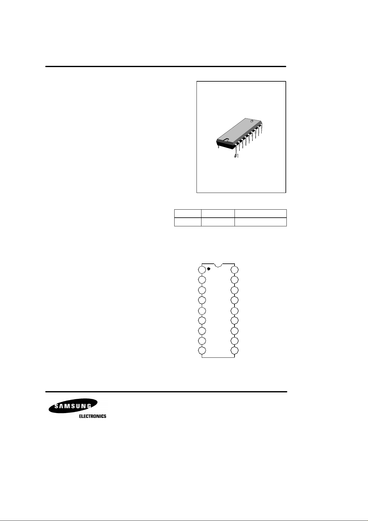
KT3170 LOW POWER DTMF RECEIVER
ORDERING INFORMATION
INTRODUCTION
18-DIP-300A
The KT3170 is a complete Dual Tone Multiple Frequency
(DTMF) receiver that is fabricated by low power CMOS
and the Switched-Capacitor Filter technology.
This LSI consists of band split filters, which seperates
counting section which verifies the frequency and
duration of the received tones before passing the corresponding code to the output bus. It decodes all 16
DTMF tone pairs into a 4bits digital code.
The externally required components are minimized by
on chip provision of a differential input AMP, clock
oscillator and latched three state interface. The on chip
clock generator requires only a low cost TV cystal as
an external component.
FEATURES
• Detects all 16 standard tones.
• Low power consumption : 15mW (Typ)
• Single power supply : 5V
• Uses inexpensive 3.58MHz crystal
• Three state outputs for microprocessor interface
• Good quality and performance for using in
exchange system
Device Package Operating
KT3170N 18-DIP-300A
• Power down mode/input inhibit
APPLICATIONS PIN CONFIGURATION
• PABX
• Central Office
• Paging Systems
• Remote Control
• Credit Card Systems
• Key Phone System
• Answering Phone
• Home Automation System
• Mobile Radio
• Remote Data Entry
IN+
1
2
IN-
GS
3
V
4
REF
I
5
IN
6
PDN
7
OSC1
OSC2
8
GND
9 10
KT3170
V
DD
18
17
SI/GTO
ESO
16
DSO
15
Q4
14
13
Q3
12
Q2
Q1
11
OE
- 25°C ~ + 75°C
Fig. 1
Page 2
KT3170 LOW POWER DTMF RECEIVER
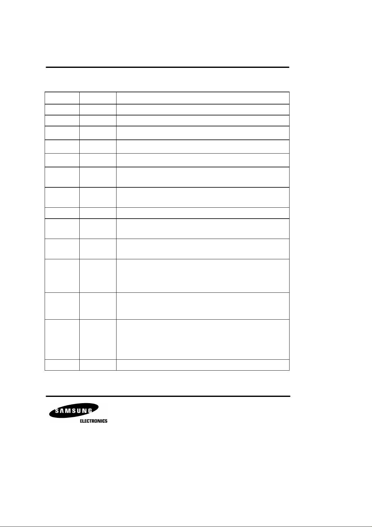
PIN DESCRIPTION
Pin No Symbol Description
1 IN + Non inverting input of the op amp.
2 IN - Inverting input of the op amp.
3 GS
4 V
5 I
REF
IN
6 PDN
7, 8
OSC1
OSC2
9 GND Ground pin.
10 OE
11 - 14 Q1 - Q4
15 DSO
16 ESO
17 SI/GTO
18 V
DD
Gain Select. The output used for gain adjustment of analog input
signal with a feedback resistor.
Reference Voltage output (VDD/2, Typ) can be used to bias the op amp
input of VDD/2.
Input inhibit. High input states inhibits the detection of tones. This
pin is pulled down internally.
Control input for the stand-by power down mode. Power down occurs
when the signal on this input is in high states. This pin is pulled down
internally.
Clock input/output. A inexpensive 3.579545MHz crystal connected
between these pins completes internal oscillator. Also, external clock
can be used.
Output Enable input. Outputs Q1-Q4 are CMOS push pull when OE is
High and open circuited (High impedance) when disabled by pulling OE
low. Internal pull up resistor built in.
Three state data output. When enabled by OE, these digital outputs
provide the hexadecimal code corresponding to the last valid tone
pair received.
Delayed Steering Output. Indicates that valid frequencies have been
present for the required guard time, thus constituting a valid signal.
Presents a logic high when a received tone pair has been registered
and the output latch is updated. Returns to logic low when the
voltage on SI/GTO falls below VTH.
Early Steering Outputs. Indicates detection of valid tone output a
logic high immediately when the digital algorithm detects a
recognizable tone pair. Any momentary loss of signal condition will
cause ESO to return to low.
Steering Input/Guard Time Output. A voltage greater the V
TS
detected at SI causes the device to register the detected tone pair
and update the output latch. A voltage less than VTS frees the device
to accept a new tone pair. The GTO output acts to reset the external
steering time constant, and its state is a function of ESO and the
voltage on SI
Power Supply (+5V, Typ)
Page 3

KT3170 LOW POWER DTMF RECEIVER
ABSOLUTE MAXIMUM RATINGS
Characteristics Symbol Value Unit
Power Supper Voltage
Analog Input Voltage Range
Digital Input Voltage Range
Output Voltage Range
Current On Any Pin
Operating Temperature
Storage Temperature
ELECTRICAL CHARACTERISTICS (V
V
DD
V
I (A)
V
I (D)
V
O
I
I
T
OPR
T
STG
= 5V, Ta = 25°C, unless otherwise noted)
DD
6
- 0.3 ~ VDD + 0.3
- 0.3 ~ VDD + 0.3
- 0.3 ~ VDD + 0.3
10
- 40 ~ + 85
-60 ~ + 150
V
V
V
V
mA
°C
°C
Characteristic Symbol Test Conditions Min Typ Max Unit
Operating Voltage V
Operating Current I
Power Dissipation P
Input Voltage Low V
Input Voltage High V
Input Leakage Current I
Pull Up Current On OE Pin I
DD
DD
D
IL
IH
I (LKG)
PU
Analog Input Impedance R
Steering Input Threshold Voltage V
Output Voltage Low V
- V
Output Current I
Output Current I
V
Output Voltage V
REF
V
Output Resistance R
REF
Analog Input Offset Voltage V
TH
OL
OH
O (SINK)
O (SOURCE)VOH
O (REF)
O (REF)
IO
Power Supply Rejection Ratio PSRR
VIN = GND or V
OE = GND - 7.5 15
fIN = 1KHz 8 10 -
I
No Load - - 0.03 V
No Load 4.97 - V
VOL = 0.4V 1 2.5 - mA
Gain Setting Amp
at 1KHz
- 4.75 - 5.25 V
- - 3.0 9.0 mA
- - 15 45 mW
- - - 1.5 V
- 3.5 - - V
DD
- 0.1 -
- 2.2 - 2.5 V
= 4.6V 0.4 0.8 - mA
- 2.4 - 2.8 V
- - 10 -
- - 25 - mV
-
60
-
Common Mode Rejection Ratio CMRR - 3.0V < VIN < 3.0V - 60 - dB
Open Loop Voltage Gain G
Gain Setting Amp at 1KHz - 65 - dB
V
Open Loop Unit Gain Bandwidth BW - - 1.5 - MHz
Analog Output Voltage Swing V
Acceptable Capacitive Load C
Acceptable Resistive Load R
Analog Input Common Mode
Voltage Range
O (P-P)
V
CM
RL = 100K - 4.5 - V
GS - 100 - pF
L
GS - 50 -
L
No Load
-
3.0
-
µA
µA
MΩ
KΩ
dB
KΩ
V
P-P
P-P
Page 4
KT3170 LOW POWER DTMF RECEIVER
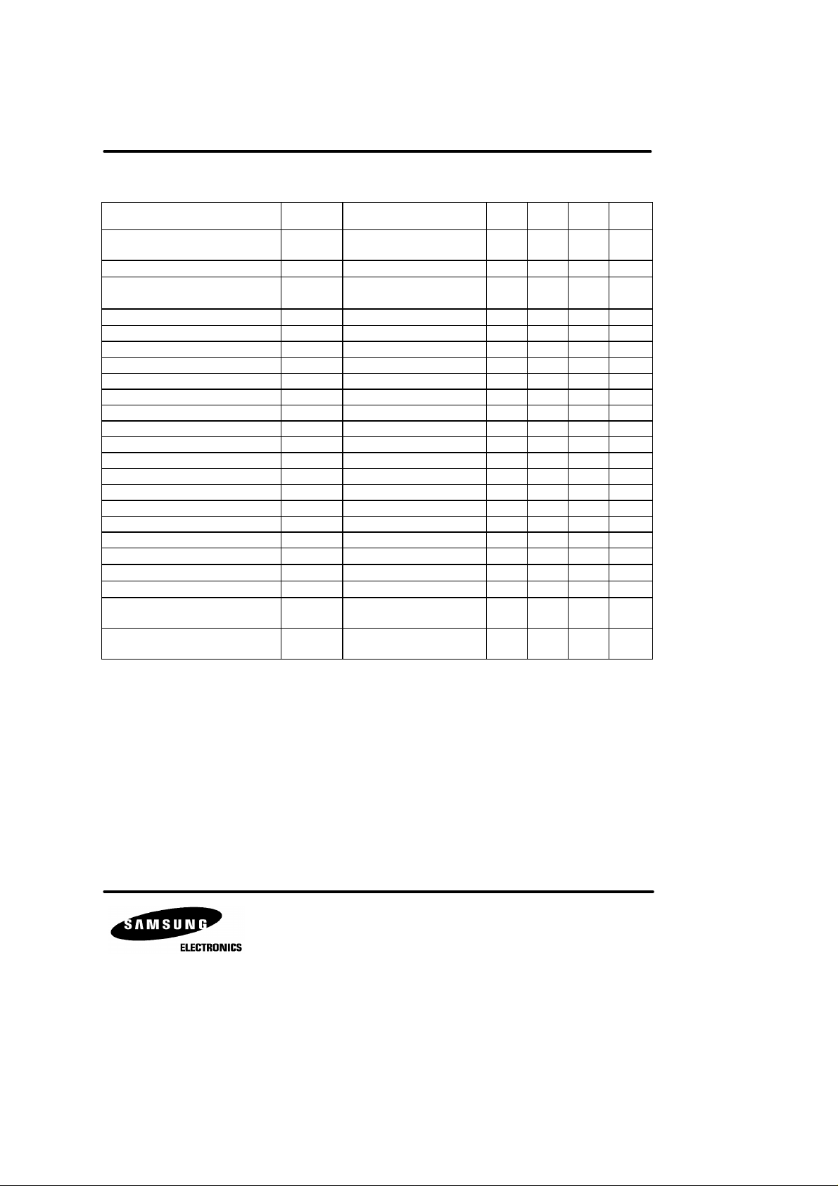
AC ELECTRICAL CHARACTERISTICS (V
= 5V, Ta = 25°C, fCK = 3.579545MHz)
DD
Characteristic Symbol Test Conditions Min Typ Max Unit
Valid Input Signal Range
(each tone of composite signal)
Dual Tone Twist Accept TW - -
Acceptable Frequency Deviation
Frequency Deviation Reject
V
I (VAL)
∆f
∆f
- -
- - -
R
-
-29 1.0
± 10
± 3.5%
- - -
- dB
± 1.5%
± 2Hz
Third Tone Tolerance T3rd - -25 -16 - dB
Noise Tolerance T
N
- - -12 - dB
Dial Tolerance DT - 18 22 - dB
Crystal Clock Frequency f
Maximum Clock Input Rise Time t
Maximum Clock Input Fall Time t
R (MAX)
F (MAX)
Acceptable Clock Input Duty Cycle D
Acceptable Capacitive Load C
Tone Present Detect Time t
Tone Absent Detect Time t
Minimum Tone Duration Accept t
Maximum Tone Duration Reject t
DET (P)
DET (A)
TDA (MIN)
TDR (MAX)
Acceptable Interdigit Pause t
Rejectable Interdigit Pause t
Propagation Delay Time SI to Q t
Propagation Delay Time SI to DSO t
D (SI-Q)
D (SI-D)
Output Data Setup Q to DSO t
Propagation Delay Time OE to Q
(Enable)
Propagation Delay Time OE to Q
(disable)
t
D (QE-Q) EN
t
D (OE-Q) DIS
CK
CK
L
IDP (A)
IDP (R)
SU
- 3.5759 3.5795 3.5831 MHz
External Clock - - 110 nS
External Clock - - 110 nS
External Clock 40 50 60 %
OSC2 PIN - - 30 pF
- 5 11 14 mS
- 0.5 4 8.5 mS
User Adjustable - - 40 mS
User Adjustable 20 - - mS
User Adjustable - - 40 mS
User Adjustable 20 - - mS
OE = High - 8 11
OE = High - 12 16
OE = High - 3.4 -
RL = 10K, CL = 50pF
RL = 10K, CL = 50pF
-
50
- -
300
60
dBm
-
µS
µS
µS
nS
nS
Notes : 1. Digit sequence consists of all 16 DTMF tones.
2. Tone duration = 40mS, Tone pause = 40mS.
3. Nominal DTMF frequencies are used.
4. Both tones in the composite signal have an equal amplitude.
5. Tone pair is deviated by ± 1.5% ± 2Hz.
6. Bandwidth limited (3KHz) Gaussian Noise.
7. The precise dial tone frequencies are (350Hz and 440Hz) ± 2%.
8. For an error rate of better than 1 in 10000.
9. Referenced to lowest level frequency component in DTMF signal.
10. Minimum signal acceptance level is measured with specitied maximum frequency deviation.
11. This item also applies to a third tone injected onto the power supply.
12. Referenced to Fig. 1 Input DTMF tone level at -28dBm.
Page 5
KT3170 LOW POWER DTMF RECEIVER
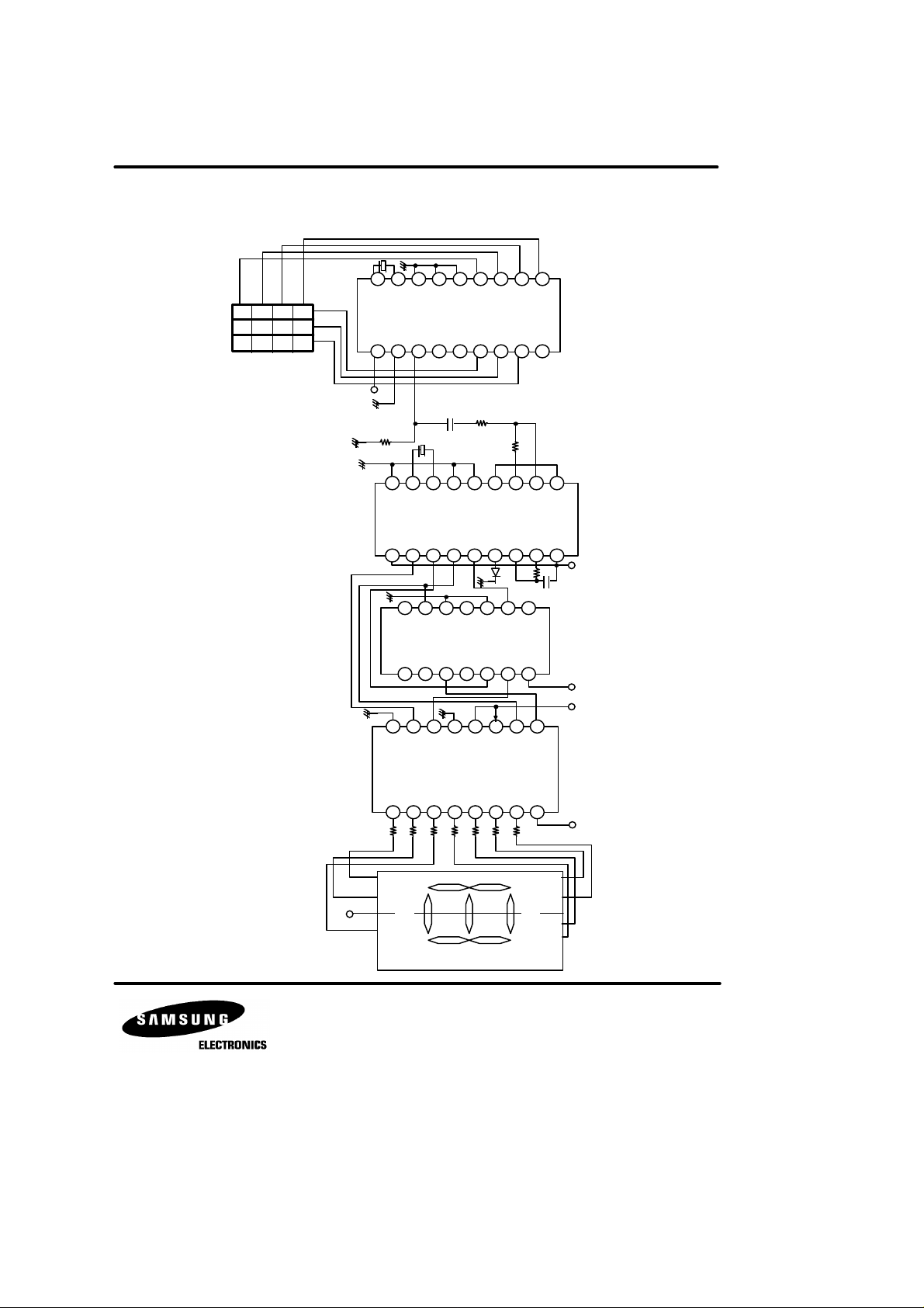
TEST CIRCUIT
9
8
6
5
4
3
15
R1
100K
2
16
17
181
100K
R2
1
2
3
4
18
17
16
15
300K
LED
1
2
3
V
CC
R3
C1
X - tal 1
4 5 6
7 8 9
*
0
#
321
V
CC
7
KS58006
10
11
12
13
14
0.1µF
X - tal 2
5
6
7
8
9 10
KT3170
14
13
12
11
7
4
5
6
Fig. 2
HL74HCTLS02
14
12
11
8
GND
8
9
6
5
7
ABI
d
4
RDO
13
3
c
LT
V
CC
V
CC
1102
b
HL74LS47
d
13
12
11
10
9
R6
R5
R4
a
1
2 3
V
CC
comd
4 5
c dp
R9
R8
R7
CC
f
16
15
14
R10
g
f
com
V
CC
10
9 8 7 6
a b
V
g
a
c
LTS542R
Page 6
KT3170 LOW POWER DTMF RECEIVER
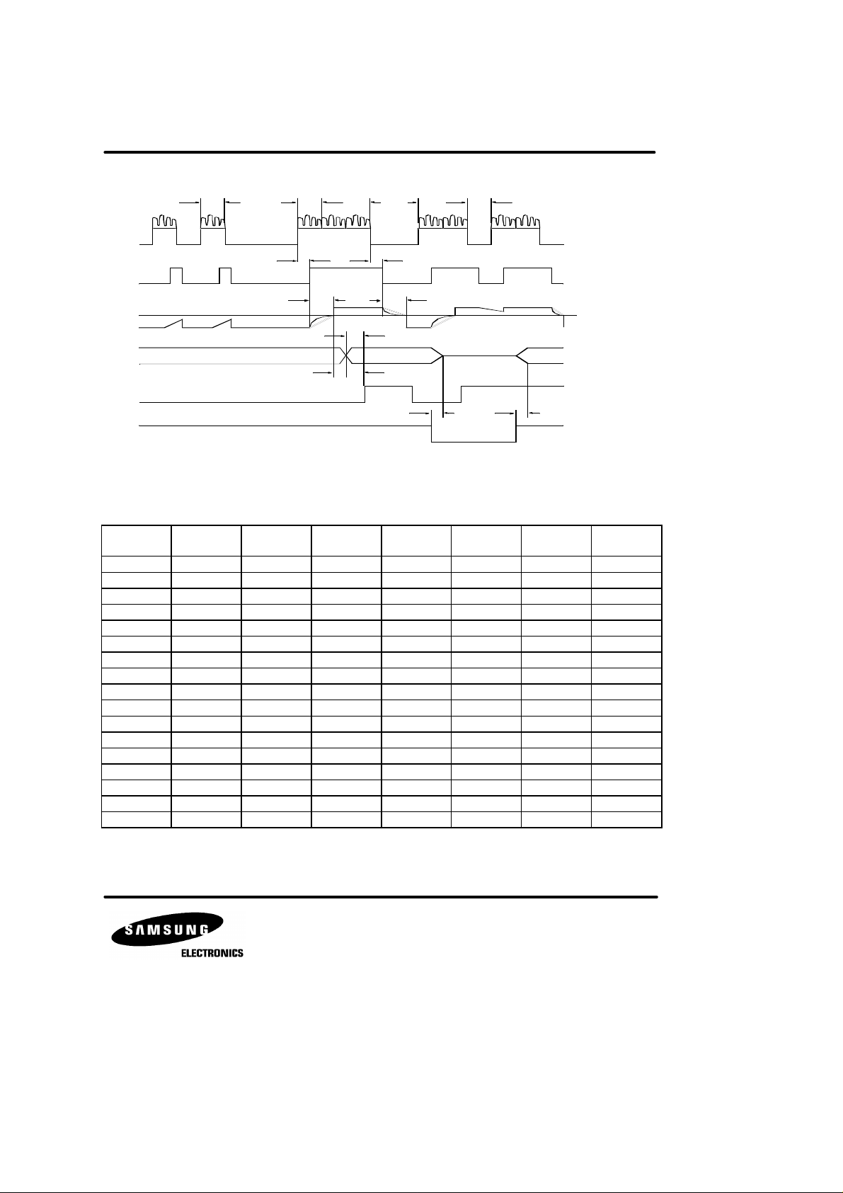
TIMING DIAGRAM
t
TDR (MAX)
DTMF
INPUT
ESO
SI/GTO
Q1 - Q4
DSO
DECODED TONE # (n - 1)
OE
t
TDA (MIN)
t
DET (P)
DTMF #n DTMF #n + 1
t
PGT
t
D (SI-D)
t
IDP (A)
t
t
IDP (R)
DTMF #n + 1
t
DET (A)
t
AGT
SU
t
D (OE-Q) EN
t
D (OE-Q) DIS
V
TH
Fig. 3
DIGITAL OUTPUT
Outputs Q1-Q4 are CMOS push pull when enabled (EO = High) and open circuited (high impedance) when disabled
by pulling EO = Low. These digital outputs provide the hexadecimal code corresponding to the DTMF signals. The table
below describes the hexadecimal.
NO
LOW
FREQUENCY
1 697 1209 H 0 0 0 1
2 697 1336 H 0 0 1 0
3 697 1477 H 0 0 1 1
4 770 1209 H 0 1 0 0
5 770 1336 H 0 1 0 1
6 770 1477 H 0 1 1 0
7 852 1209 H 0 1 1 1
8 852 1336 H 1 0 0 0
9 852 1477 H 1 0 0 1
0 941 1336 H 1 0 1 0
* 941 1209 H 1 0 1 1
# 941 1477 H 1 1 0 0
A 697 1633 H 1 1 0 1
B 770 1633 H 1 1 1 0
C 852 1633 H 1 1 1 1
D 941 1633 H 0 0 0 0
ANY - - L Z Z Z Z
Z : High Impedance
H : High Logic Level
L : Low Logic Level
HIGH
FREQUENCY
OE Q4 Q3 Q2 Q1
Page 7
KT3170 LOW POWER DTMF RECEIVER
2
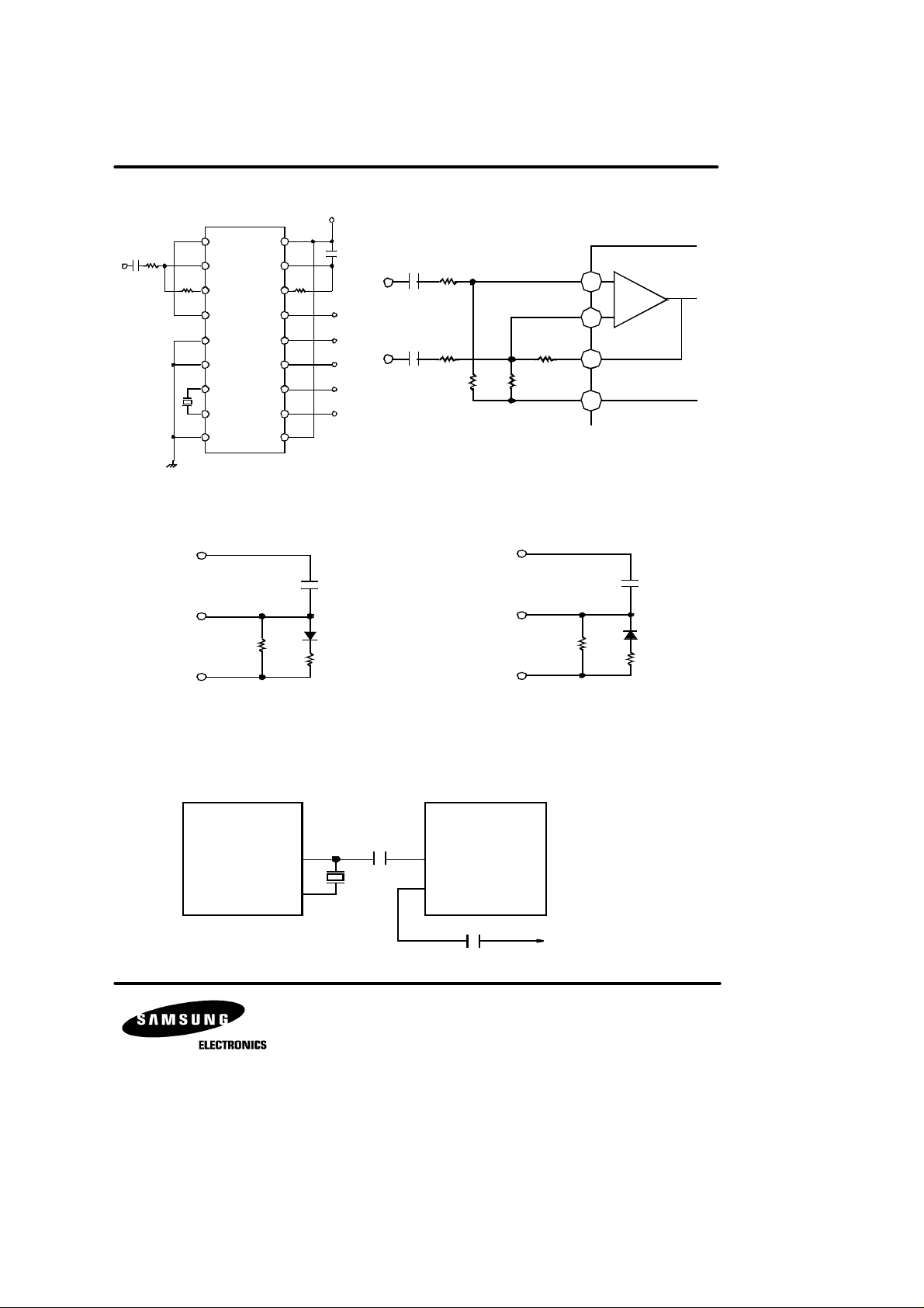
APPLICATION CIRCUIT
100K
3.58MHz
IN+
IN-
GS
V
REF
I
IN
PDN
OSC1
OSC2
GND
0.1uF
100K
V
SI/GTO
ESO
DSO
+5V
DD
0.1uF
300K
Q4
Q3
Q2
Q1
OE
R3 = R2R5/(R2+R5), VOLTAGE GAIN = R5/R1
INPUT IMPEDANCE : 2 + (1/wC)
All resistors are 1% tolerance
10nF
C1 R1
10nF
C2 R2
100K
100K
R3
37.5KR260K
R5
100K
V
√R
REF
IN+
IN-
GS
1
1
+
_
2
3
KT3170
4
2
All resistors are 1% tolerance All capacitors are 5% tolerance
All capacitors are 5% tolerance
Fig. 4 Single Ended Input Configuration Fig. 5 Differential Ended Input Configuration
V DD
C
R2
SI/GTO
ESO
C
SI/GTO
R1
R2
ESO
R1
t
t
RP = R1R2/(R1 + R2) RP = R1R2 (R1 + R2)
(a) Decreasing t
= (R1C) In (VDD/VDD-VTH) t
PGT
= (RPC) In (VDD/V
AGT
) t
TST
(t
> t
AGT
) (a) Decreasing t
PGT
AGT
= (RPC) In (VDD/VDD-VTH)
PGT
= (R1C) In (VDD/VTH)
AGT
(t
PGT
Fig. 6 Guard Time Adjustment
KT3170
OSC1
OSC2
30pF
3.579545MHz
KT3170
OSC1
OSC2
TO OSC1 of next KT3170
Fig. 7 Oscillator Connection
PGT
< t
)
AGT
 Loading...