

Page 1
KSZ8041TL/FTL
10Base-T/100Base-TX/100Base-FX
Physical Layer Transceiver
General Description
The KSZ8041TL is a single supply 10Base-T/100Base-TX
Physical Layer Transceiver, which provides MII/RMII/SMII
interfaces to transmit and receive data. It utilizes a unique
mixed-signal design to extend signaling distance while
reducing power consumption.
HP Auto MDI/MDI-X provides the most robust solution for
eliminating the need to differentiate between crossover
and straight-through cables.
Micrel LinkMD
identification of faulty copper cabling.
®
TDR-based cable diagnostics permit
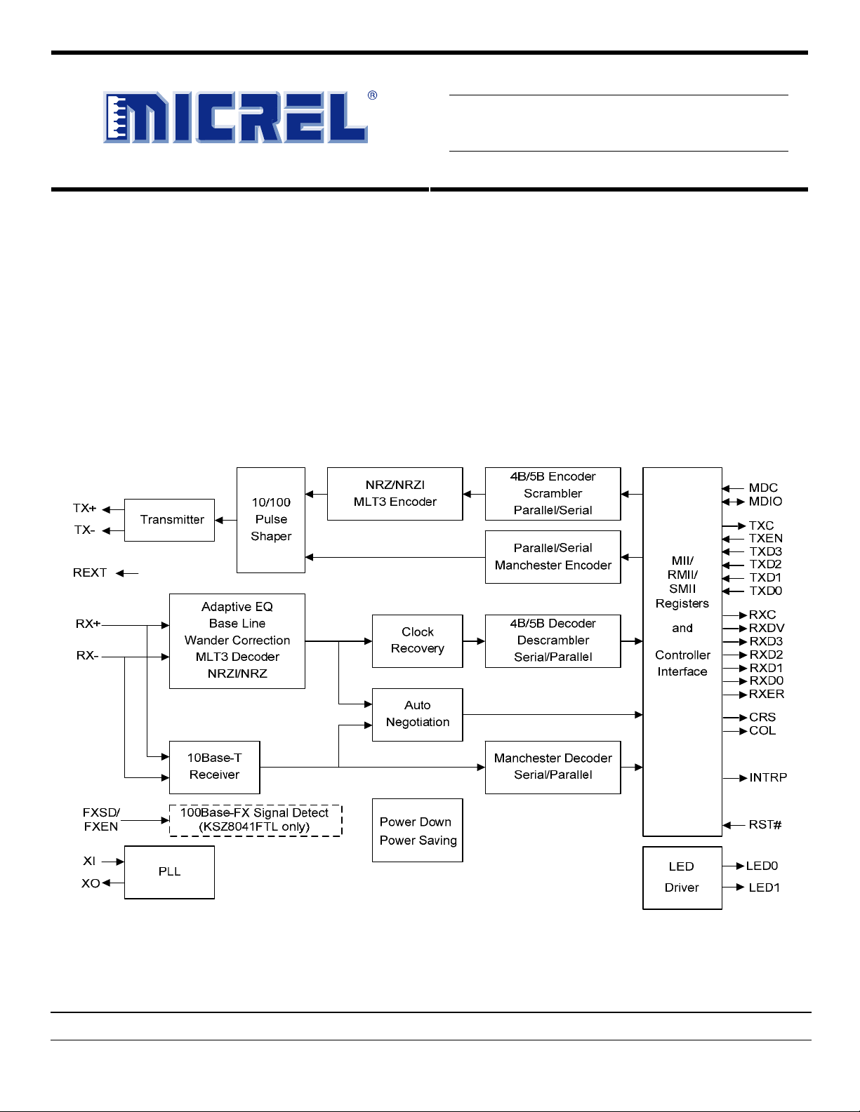
Functional Diagram
Data Sheet Rev. 1.1
The KSZ8041TL represents a new level of features and
performance and is an ideal choice of physical layer
transceiver for 10Base-T/100Base-TX applications.
The KSZ8041FTL has all the identical rich features of the
KSZ8041TL plus 100Base-FX support for fiber and media
converter applications.
Both KSZ8041TL and KSZ8041FTL are available in 48pin, lead-free TQFP packages (See Ordering Information).
Data sheets and support documentation can be found on
Micrel’s web site at: www.micrel.com.
LinkMD is a registered trademark of Micrel, Inc.
Micrel Inc. • 2180 Fortune Drive • San Jose, CA 95131 • USA • tel +1 (408) 944-0800 • fax + 1 (408) 474-1000 • http://www.micrel.com
April 2007
M9999-042707-1.1
Page 2

Micrel, Inc. KSZ8041TL/FTL
Features
Applications
• Single-chip 10Base-T/100Base-TX physical layer
solution
• Fully compliant to IEEE 802.3u Standard
• Low power CMOS design, power consumption of
<180mW
• HP auto MDI/MDI-X for reliable detection and correction
for straight-through and crossover cables with disable
and enable option
• Robust operation over standard cables
®
• LinkMD
TDR-based cable diagnostics for identification
of faulty copper cabling
• Fiber support: 100Base-FX (KSZ8041FTL only), Backto-Back mode (KSZ8041FTL and KSZ8041TL)
• MII interface support
• RMII interface support with external 50MHz system
clock
• SMII interface support with external 125MHz system
clock and 12.5MHz sync clock from MAC
• MIIM (MDC/MDIO) management bus to 12.5MHz for
rapid PHY register configuration
• Interrupt pin option
• Programmable LED outputs for link, activity and speed
• Power down and power saving modes
• Single power supply (3.3V)
• Built-in 1.8V regulator for core
• Available in 48-pin TQFP
package
• Printer
• LOM
• Game Console
• IPTV
• IP Phone
• IP Set-top Box
• Media Converter
Ordering Information
Part Number Temp. Range Package Lead Finish
KSZ8041TL 0°C to 70°C 48-Pin TQFP Pb-Free
KSZ8041TLI
KSZ8041FTL 0°C to 70°C 48-Pin TQFP Pb-Free
KSZ8041FTLI
Note:
1. Contact factory for lead time.
(1)
-40°C to 85°C 48-Pin TQFP Pb-Free
(1)
-40°C to 85°C 48-Pin TQFP Pb-Free
April 2007 2
M9999-042707-1.1
Page 3

Micrel, Inc. KSZ8041TL/FTL
Revision History
Revision Date Summary of Changes
1.0 12/21/06 Data sheet created.
1.1 4/27/07 Added maximum MDC clock speed.
Added 40K +/-30% to note 1 of Pin Description and Strapping Options tables for internal pull-ups/p ull-
downs.
Changed Model Number in Register 3h – PHY Identifier 2.
Changed polarity (swapped definition) of DUPLEX strapping pin.
Removed DUPLEX strapping pin update to Register 4h – Auto-Negotiation Advertisement bits [8, 6].
Added Back-to-Back mode for KSZ8041TL.
Added Symbol Error to MII/RMII Receive Error description and Register 15h – RXER Counter.
Added a 100pF capacitor on REXT (pin 16) in Pin Description table.
April 2007 3
M9999-042707-1.1
Page 4

Micrel, Inc. KSZ8041TL/FTL
Contents
Pin Configuration..................................................................................................................................................................8
Pin Description....................................................................................................................................................................10
Strapping Options...............................................................................................................................................................15
Functional Description.......................................................................................................................................................17
100Base-TX Transmit.......................................................................................................................................................17
100Base-TX Receive........................................................................................................................................................17
PLL Clock Synthesizer......................................................................................................................................................17
Scrambler/De-scrambler (100Base-TX only)....................................................................................................................17
10Base-T Transmit...........................................................................................................................................................17
10Base-T Receive............................................................................................................................................................18
SQE and Jabber Function (10Base-T only)......................................................................................................................18
Auto-Negotiation...............................................................................................................................................................18
MII Management (MIIM) Interface....................................................................................................................................20
Interrupt (INTRP)..............................................................................................................................................................20
MII Data Interface.............................................................................................................................................................20
MII Signal Definition..........................................................................................................................................................21
Transmit Clock (TXC).................................................................................................................................................21
Transmit Enable (TXEN).............................................................................................................................................21
Transmit Data [3:0] (TXD[3:0])...................................................................................................................................21
Receive Clock (RXC)..................................................................................................................................................21
Receive Data Valid (RXDV)........................................................................................................................................22
Receive Data [3:0] (RXD[3:0])....................................................................................................................................22
Receive Error (RXER).................................................................................................................................................22
Carrier Sense (CRS) ...................................................................................................................................................22
Collision (COL) ...........................................................................................................................................................22
Reduced MII (RMII) Data Interface...................................................................................................................................22
RMII Signal Definition.......................................................................................................................................................23
Reference Clock (REF_CLK) .....................................................................................................................................23
Transmit Enable (TX_EN)...........................................................................................................................................23
Transmit Data [1:0] (TXD[1:0])...................................................................................................................................23
Carrier Sense/Receive Data Valid (CRS_DV)...........................................................................................................23
Receive Data [1:0] (RXD[1:0])....................................................................................................................................23
Receive Error (RX_ER)...............................................................................................................................................23
Collision Detection.....................................................................................................................................................24
Serial MII (SMII) Data Interface........................................................................................................................................24
SMII Signal Definition .......................................................................................................................................................24
Clock Reference (CLOCK).........................................................................................................................................24
Sync Pulse (SYNC).....................................................................................................................................................24
Transmit Data and Control (TX) ................................................................................................................................24
Receive Data and Control (RX)..................................................................................................................................25
Collision Detection.....................................................................................................................................................26
HP Auto MDI/MDI-X..........................................................................................................................................................27
Straight Cable .............................................................................................................................................................27
Crossover Cable.........................................................................................................................................................28
LinkMD® Cable Diagnostics..............................................................................................................................................29
Access.........................................................................................................................................................................29
Usage...........................................................................................................................................................................29
April 2007 4
M9999-042707-1.1
Page 5

Micrel, Inc. KSZ8041TL/FTL
Power Management..........................................................................................................................................................29
Power Saving Mode....................................................................................................................................................29
Power Down Mode......................................................................................................................................................29
Reference Clock Connection Options ..............................................................................................................................30
Reference Circuit for Power and Ground Connections....................................................................................................31
100Base-FX Fiber Operation (KSZ8041FTL only)...........................................................................................................32
Fiber Signal Detect.....................................................................................................................................................32
Far-End Fault...............................................................................................................................................................32
Back-to-Back Media Converter.........................................................................................................................................33
MII Back-to-Back Mode..............................................................................................................................................33
RMII Back-to-Back Mode............................................................................................................................................34
Register Map........................................................................................................................................................................35
Register Description...........................................................................................................................................................35
Absolute Maximum Ratings
Operating Ratings
(2)
............................................................................................................................................................43
Electrical Characteristics
(1)
............................................................................................................................................43
(3)
................................................................................................................................................43
Timing Diagrams.................................................................................................................................................................45
MII SQE Timing (10Base-T) .............................................................................................................................................45
MII Transmit Timing (10Base-T).......................................................................................................................................46
MII Receive Timing (10Base-T)........................................................................................................................................47
MII Transmit Timing (100Base-TX) ..................................................................................................................................48
MII Receive Timing (100Base-TX) ...................................................................................................................................49
RMII Timing.......................................................................................................................................................................50
Auto-Negotiation Timing...................................................................................................................................................51
MDC/MDIO Timing ...........................................................................................................................................................52
Reset Timing.....................................................................................................................................................................53
Reset Circuit........................................................................................................................................................................54
Selection of Isolation Transformer....................................................................................................................................56
Selection of Reference Crystal..........................................................................................................................................56
Package Information...........................................................................................................................................................57
April 2007 5
M9999-042707-1.1
Page 6

Micrel, Inc. KSZ8041TL/FTL
List of Figures
Figure 1. Auto-Negotiation Flow Chart.................................................................................................................................19
Figure 2. SMII Transmit Data/Control Segment...................................................................................................................25
Figure 3. SMII Receive Data/Control Segment....................................................................................................................26
Figure 4. Typical Straight Cable Connection .......................................................................................................................27
Figure 5. Typical Crossover Cable Connection ...................................................................................................................28
Figure 6. 25MHz Crystal / Oscillator Reference Clock for MII Mode...................................................................................30
Figure 7. 50MHz Oscillator Reference Clock for RMII Mode...............................................................................................30
Figure 8. 125MHz Oscillator Reference Clock for SMII Mode.............................................................................................30
Figure 9. KSZ8041TL/FTL Power and Ground Connections...............................................................................................31
Figure 10. KSZ8041FTL / KSZ8041TL Back-to-Back Media Converter..............................................................................33
Figure 11. MII SQE Timing (10Base-T) ...............................................................................................................................45
Figure 12. MII Transmit Timing (10Base-T).........................................................................................................................46
Figure 13. MII Receive Timing (10Base-T)..........................................................................................................................47
Figure 14. MII Transmit Timing (100Base-TX).....................................................................................................................48
Figure 15. MII Receive Timing (100Base-TX)......................................................................................................................49
Figure 16. RMII Timing – Data Received from RMII............................................................................................................50
Figure 17. RMII Timing – Data Input to RMII.......................................................................................................................50
Figure 18. Auto-Negotiation Fast Link Pulse (FLP) Timing .................................................................................................51
Figure 19. MDC/MDIO Timing..............................................................................................................................................52
Figure 20. Reset Timing.......................................................................................................................................................53
Figure 21. Recommended Reset Circuit..............................................................................................................................54
Figure 22. Recommended Reset Circuit for Interfacing with CPU/FPGA Reset Output .....................................................54
Figure 23. Reference Circuits for LED Strapping Pins.........................................................................................................55
April 2007 6
M9999-042707-1.1
Page 7

Micrel, Inc. KSZ8041TL/FTL
List of Tables
Table 1. MII Management Frame Format............................................................................................................................20
Table 2. MII Signal Definition...............................................................................................................................................21
Table 3. RMII Signal Description..........................................................................................................................................23
Table 4. SMII Signal Description..........................................................................................................................................24
Table 5. SMII TX Bit Description..........................................................................................................................................25
Table 6. SMII TXD[0:7] Encoding Table ..............................................................................................................................25
Table 7. SMII RX Bit Description..........................................................................................................................................26
Table 8. SMII RXD[0:7] Encoding Table..............................................................................................................................26
Table 9. MDI/MDI-X Pin Definition.......................................................................................................................................27
Table 10. KSZ8041TL/FTL Power Pin Description..............................................................................................................31
Table 11. Copper and Fiber Mode Selection.......................................................................................................................32
Table 12. MII Signal Connection for MII Back-to-Back Mode..............................................................................................33
Table 13. RMII Signal Connection for RMII Back-to-Back Mode.........................................................................................34
Table 14. MII SQE Timing (10Base-T) Parameters.............................................................................................................45
Table 15. MII Transmit Timing (10Base-T) Parameters ......................................................................................................46
Table 16. MII Receive Timing (10Base-T) Parameters .......................................................................................................47
Table 17. MII Transmit Timing (100Base-TX) Parameters..................................................................................................48
Table 18. MII Receive Timing (100Base-TX) Parameters...................................................................................................49
Table 19. RMII Timing Parameters......................................................................................................................................50
Table 20. Auto-Negotiation Fast Link Pulse (FLP) Timing Parameters...............................................................................51
Table 21. MDC/MDIO Timing Parameters...........................................................................................................................52
Table 22. Reset Timing Parameters ....................................................................................................................................53
Table 23. Transformer Selection Criteria.............................................................................................................................56
Table 24. Qualified Single Port Magnetics...........................................................................................................................56
Table 25. Typical Reference Crystal Characteristics...........................................................................................................56
April 2007 7
M9999-042707-1.1
Page 8

Micrel, Inc. KSZ8041TL/FTL
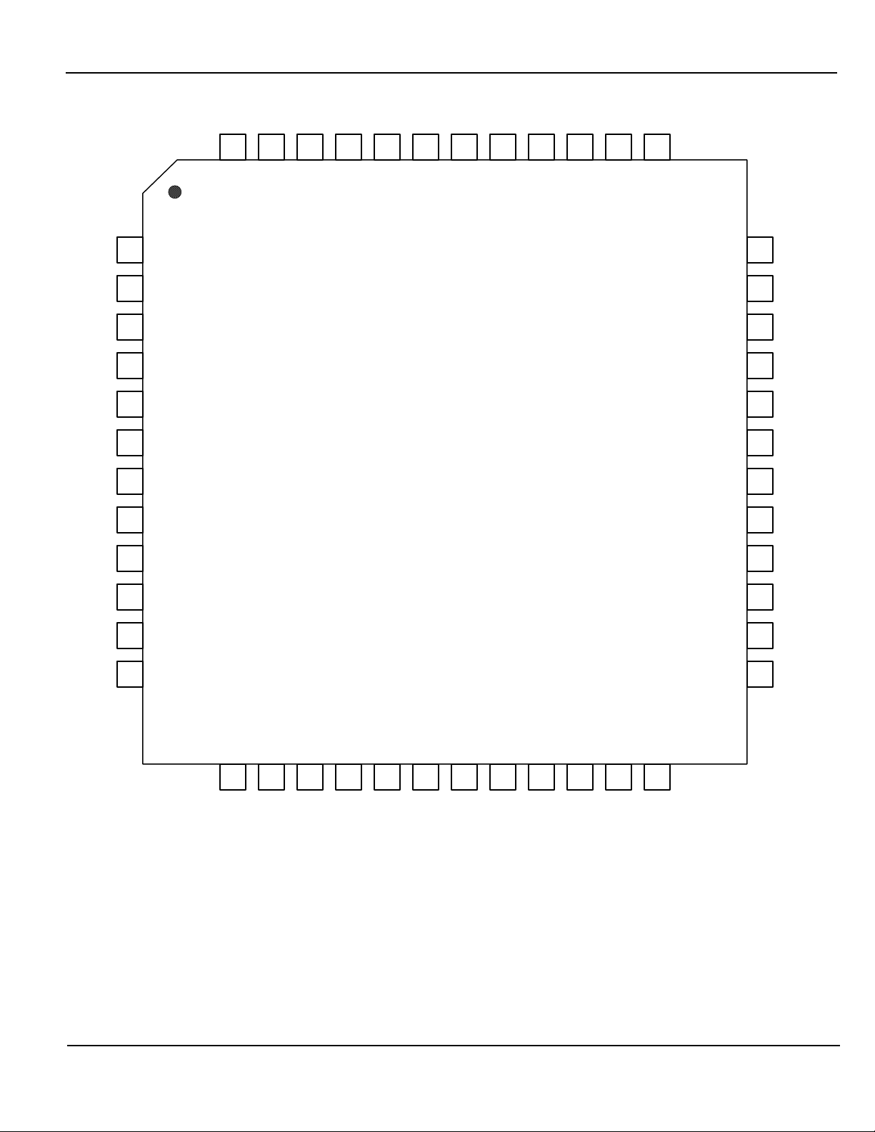
Pin Configuration
1
2
3
4
5
6
7
8
9
GND
GND
GND
VDDA_1.8
VDDA_1.8
V1.8_OUT
VDDA_3.3
VDDA_3.3
RX-
NC
RST#
NC
NC
NC
LED1 /
SPEED
KSZ8041TL
4142434445464748
COL /
CRS /
LED0 /
NWAYEN
CONFIG1
TXD3
CONFIG0
37383940
GND
TXD2
TXD1 / TXD[1] /
TXD0 / TXD[0] /
RXER / RX_ER /
SYNC
TX
TXEN /
TX_EN
TXC
INTRP
VDD_1.8
GND
ISO
RXC
36
35
34
33
32
31
30
29
28
RXD0 / RXD[0] / RX
DUPLEX
24
RXDV / CRSDV /
CONFIG2
VDDIO_3.3
VDDIO_3.3
GND
27
26
25
10
11
12
RX+
TX-
TX+
GND
XO
XI / REFCLK /
13 14 16 17
15
REXT
CLOCK
MDIO
GND
18 19 20
RXD3 /
MDC
PHYAD0
RXD2 /
PHYAD1
21 22 23
RXD1 / RXD[1] /
PHYAD2
48-Pin TQFP
April 2007 8
M9999-042707-1.1
Page 9
Micrel, Inc. KSZ8041TL/FTL
1
2
3
4
5
6
7
8
9
GND
GND
GND
VDDA_1.8
VDDA_1.8
V1.8_OUT
VDDA_3.3
VDDA_3.3
RX-
FXEN
FXSD /
RST#
NC
NC
NC
LED1 /
LED0 /
SPEED / no FEF
KSZ8041FTL
NWAYEN
4142434445464748
CRS /
CONFIG1
COL /
CONFIG0
37383940
TXD3
GND
TXD2
TXD1 / TXD[1] /
TXD0 / TXD[0] /
RXER / RX_ER /
SYNC
TX
TXEN /
TX_EN
TXC
INTRP
VDD_1.8
GND
ISO
RXC
36
35
34
33
32
31
30
29
28
RXD0 / RXD[0] / RX
DUPLEX
24
RXDV / CRSDV /
CONFIG2
VDDIO_3.3
VDDIO_3.3
GND
27
26
25
10
11
12
RX+
TX-
TX+
GND
XO
XI / REFCLK /
13 14 16 17
15
REXT
CLOCK
MDIO
GND
18 19 20
RXD3 /
MDC
PHYAD0
RXD2 /
PHYAD1
21 22 23
RXD1 / RXD[1] /
PHYAD2
48-Pin TQFP
April 2007 9
M9999-042707-1.1
Page 10

Micrel, Inc. KSZ8041TL/FTL
Pin Description
Pin Number Pin Name
1 GND Gnd Ground
2 GND Gnd Ground
3 GND Gnd Ground
4 VDDA_1.8 P 1.8V analog VDD
5 VDDA_1.8 P 1.8V analog VDD
6 V1.8_OUT P 1.8V output voltage from chip
7 VDDA_3.3 P 3.3V analog VDD
8 VDDA_3.3 P 3.3V analog VDD
9 RX- I/O Physical receive or transmit signal (- differential)
10 RX+ I/O Physical receive or transmit signal (+ differential)
11 TX- I/O Physical transmit or receive signal (- differential)
12 TX+ I/O Physical transmit or receive signal (+ differential)
13 GND Gnd Ground
14 XO O Crystal feedback
15 XI /
REFCLK /
CLOCK
16 REXT I/O Set physical transmit output current
17 GND Gnd Ground
18 MDIO I/O Management Interface (MII) Data I/O
19 MDC I Management Interface (MII) Clock Input
20 RXD3 /
PHYAD0
21 RXD2 /
PHYAD1
22 RXD1 /
RXD[1] /
PHYAD2
(1)
Type
Pin Function
This pin is used only in MII mode when a 25 MHz crystal is used.
This pin is a no connect if oscillator or external clock source is used, or if RMII
mode or SMII mode is selected.
I Crystal / Oscillator / External Clock Input
MII Mode: 25MHz +/-50ppm (crystal, oscillator, or external clock)
RMII Mode: 50MHz +/-50ppm (oscillator, or external clock only)
SMII Mode: 125MHz +/-100ppm (oscillator, or external clock only)
Connect a 6.49KΩ resistor in parallel with a 100pF capacitor to ground on this
pin. See KSZ8041TL-FTL reference schematics.
This pin requires an external 4.7KΩ pull-up resistor.
This pin is synchronous to the MDIO data interface.
Ipu/O
MII Mode: Receive Data Output[3]
Config Mode: The pull-up/pull-down value is latched as PHYADDR[0] during
power-up / reset. See “Strapping Options” section for details.
Ipd/O
MII Mode: Receive Data Output[2]
Config Mode: The pull-up/pull-down value is latched as PHYADDR[1] during
power-up / reset. See “Strapping Options” section for details.
Ipd/O
MII Mode: Receive Data Output[1]
RMII Mode: Receive Data Output[1]
Config Mode: The pull-up/pull-down value is latched as PHYADDR[2] during
power-up / reset. See “Strapping Options” section for details.
(2)
(2)
(2)
(3)
/
/
/
/
April 2007 10
M9999-042707-1.1
Page 11

Micrel, Inc. KSZ8041TL/FTL
Pin Number Pin Name
23 RXD0 /
RXD[0] /
RX
DUPLEX
24 GND Gnd Ground
25 VDDIO_3.3 P 3.3V digital VDD
26 VDDIO_3.3 P 3.3V digital VDD
27 RXDV /
CRSDV /
CONFIG2
28 RXC O MII Mode: Receive Clock Output
29 RXER /
RX_ER /
ISO
30 GND Gnd Ground
31 VDD_1.8 P 1.8V digital VDD
32 INTRP Opu Interrupt Output: Programmable Interrupt Output
33 TXC I/O MII Mode: Transmit Clock Output
34 TXEN /
TX_EN
35 TXD0 /
TXD[0] /
TX
36 TXD1 /
TXD[1] /
SYNC
37 GND Gnd Ground
38 TXD2 I
39 TXD3 I
40 COL /
CONFIG0
41 CRS /
CONFIG1
(1)
Type
Ipu/O
Pin Function
MII Mode: Receive Data Output[0]
RMII Mode: Receive Data Output[0]
(2)
(3)
SMII Mode: Receive Data and Control
Config Mode: Latched as DUPLEX (register 0h, bit 8) during power-up /
reset. See “Strapping Options” section for details.
Ipd/O MII Mode: Receive Data Valid Output /
RMII Mode: Carrier Sense/Receive Data Valid Output /
Config Mode: The pull-up/pull-down value is latched as CONFIG2 during
power-up / reset. See “Strapping Options” section for details.
Ipd/O MII Mode: Receive Error Output /
RMII Mode: Receive Error Output /
Config Mode: The pull-up/pull-down value is latched as ISOLATE during
power-up / reset. See “Strapping Options” section for details.
Register 1Bh is the Interrupt Control/Status Register for programming the
interrupt conditions and reading the interrupt status. Register 1Fh bit 9 sets the
interrupt output to active low (default) or active high.
MII Back-to Back Mode: Transmit Clock Input
I MII Mode: Transmit Enable Input /
RMII Mode: Transmit Enable Input
I
MII Mode: Transmit Data Input[0]
RMII Mode: Transmit Data Input[0]
(5)
(6) /
/
SMII Mode: Transmit Data and Control
I
MII Mode: Transmit Data Input[1]
RMII Mode: Transmit Data Input[1]
(5)
(6)
/
/
SMII Mode: SYNC Clock Input
MII Mode: Transmit Data Input[2]
MII Mode: Transmit Data Input[3]
(5)
(5)
/
/
Ipd/O MII Mode: Collisio n Detect Output /
Config Mode: The pull-up/pull-down value is latched as CONFIG0 during
power-up / reset. See “Strapping Options” section for details.
Ipd/O MII Mode: Carrier Sense Output /
Config Mode: The pull-up/pull-down value is latched as CONFIG1 during
power-up / reset. See “Strapping Options” section for details.
/
/
(4)
(7)
/
April 2007 11
M9999-042707-1.1
Page 12
Micrel, Inc. KSZ8041TL/FTL
Pin Number Pin Name
42
(KSZ8041TL)
42
(KSZ8041FTL)
LED0 /
NWAYEN
LED0 /
NWAYEN
April 2007 12
(1)
Type
Ipu/O LED Output: Programmable LED0 Output /
Ipu/O LED Output: Programmable LED0 Output /
Pin Function
Config Mode: Latched as Auto-Negotiation Enable (register 0h, bit 12)
during power-up / reset. See “Strapping Options” section for
details.
The LED0 pin is programmable via register 1Eh bits [15:14], and is defined as
follows.
LED mode = [00]
Link/Activity Pin State LED Definition
No Link H OFF
Link L ON
Activity Toggle Blinking
LED mode = [01]
Link Pin State LED Definition
No Link H OFF
Link L ON
LED mode = [10]
Reserved
LED mode = [11]
Reserved
Config Mode: If copper mode (FXEN=0), latched as Auto-Negotiation
Enable (register 0h, bit 12) during power-up / reset.
If fiber mode (FXEN=1), this pin configuration is always
strapped to disable Auto-Negotiation.
See “Strapping Options” section for details.
The LED0 pin is programmable via register 1Eh bits [15:14], and is defined as
follows.
LED mode = [00]
Link/Activity Pin State LED Definition
No Link H OFF
Link L ON
Activity Toggle Blinking
LED mode = [01]
Link Pin State LED Definition
No Link H OFF
Link L ON
LED mode = [10]
Reserved
LED mode = [11]
Reserved
M9999-042707-1.1
Page 13
Micrel, Inc. KSZ8041TL/FTL
Pin Number Pin Name
43
(KSZ8041TL)
43
(KSZ8041FTL)
44 NC - No connect
45 NC - No connect
46 NC - No connect
LED1 /
SPEED
LED1 /
SPEED /
no FEF
April 2007 13
(1)
Type
Ipu/O LED Output: Programmable LED1 Output /
Ipu/O LED Output: Programmable LED1 Output /
Pin Function
Config Mode: Latched as SPEED (register 0h, bit 13) during power-up /
reset. See “Strapping Options” section for details.
The LED1 pin is programmable via register 1Eh bits [15:14], and is defined as
follows.
LED mode = [00]
Speed Pin State LED Definition
10BT H OFF
100BT L ON
LED mode = [01]
Activity Pin State LED Definition
No Activity H OFF
Activity Toggle Blinking
LED mode = [10]
Reserved
LED mode = [11]
Reserved
Config Mode: If copper mode (FXEN=0), latched as SPEED (register 0h, bit
13) during power-up / reset.
If fiber mode (FXEN=1), latched as no FEF (no Far-End Fault)
during power-up / reset.
See “Strapping Options” section for details.
The LED1 pin is programmable via register 1Eh bits [15:14], and is defined as
follows.
LED mode = [00]
Speed Pin State LED Definition
10BT H OFF
100BT L ON
LED mode = [01]
Activity Pin State LED Definition
No Activity H OFF
Activity Toggle Blinking
LED mode = [10]
Reserved
LED mode = [11]
Reserved
M9999-042707-1.1
Page 14

Micrel, Inc. KSZ8041TL/FTL
Pin Number Pin Name
47 RST# I Chip Reset (active low)
48
NC - No connect
(KSZ8041TL)
48
(KSZ8041FTL)
FXSD /
FXEN
(1)
Type
Pin Function
Ipd FXSD: Signal Detect for 100Base-FX fiber mode
FXEN: Fiber Enable for 100Base-FX fiber mode
If FXEN=0, fiber mode is disabled. PHY is in copper mode. The default is “0”.
See “100Base-FX Operation” section for details.
Notes:
1. P = Power supply.
Gnd = Ground.
I = Input.
O = Output.
I/O = Bi-directional.
Ipd = Input with internal pull-down (40K +/-30%).
Ipu = Input with internal pull-up (40K +/-30%).
Opu = Output with internal pull-up (40K +/-30%).
Ipu/O = Input with internal pull-up (40K +/-30%) during power-up/reset; output pin otherwise.
Ipd/O = Input with internal pull-down (40K +/-30%) during power-up/reset; output pin otherwise.
2. MII Rx Mode: The RXD[3..0] bits are synchronous with RXCLK. When RXDV is asserted, RXD[3..0] presents valid data to MAC through the MII.
RXD[3..0] is invalid when RXDV is de-asserted.
3. RMII Rx Mode: The RXD[1:0] bits are synchronous with REF_CLK. For each clock period in which CRS_DV is asserted, two bits of recovered
data are sent from the PHY.
4. SMII Rx Mode: Receive data and control information are sent in 10 bit segments. In 100MBit mode, each segment represents a new byte of
data. In 10MBit mode, each segment is repeated ten times; therefore, every ten segments represent a new byte of data. The MAC can sample
any one of every 10 segments in 10MBit mode.
5. MII Tx Mode: The TXD[3..0] bits are synchronous with TXCLK. When TXEN is asserted, TXD[3..0] presents valid data from the MAC through
the MII. TXD[3..0] has no effect when TXEN is de-asserted.
6. RMII Tx Mode: The TXD[1:0] bits are synchronous with REF_CLK. For each clock period in which TX_EN is asserted, two bits of data are
received by the PHY from the MAC.
7. SMII Tx Mode: Transmit data and control information are received in 10 bit segments. In 100MBit mode, each segment represents a new byte
of data. In 10MBit mode, each segment is repeated ten times; therefore, every ten segments represent a new byte of data. The PHY can
sample any one of every 10 segments in 10MBit mode.
April 2007 14
M9999-042707-1.1
Page 15
Micrel, Inc. KSZ8041TL/FTL
Strapping Options
Pin Number Pin Name
22
21
20
27
41
40
29 ISO Ipd/O ISOLATE mode
43
(KSZ8041TL)
43
(KSZ8041FTL)
PHYAD2
PHYAD1
PHYAD0
CONFIG2
CONFIG1
CONFIG0
SPEED Ipu/O SPEED mode
SPEED /
no FEF
April 2007 15
(1)
Type
Ipd/O
Ipd/O
Ipu/O
Ipd/O
Ipd/O
Ipd/O
Ipu/O If copper mode (FXEN=0), pin strap-in is SPEED mode.
Pin Function
The PHY Address is latched at power-up / reset and is configurable to any value from
1 to 7.
The default PHY Address is 00001.
PHY Address bits [4:3] are always set to ‘00’.
The CONFIG[2:0] strap-in pins are latched at power-up / reset and are defined as
follows:
CONFIG[2:0] Mode
000 MII (default)
001 RMII
010 SMII
011 Reserved – not used
100 PCS Loopback
101 RMII back-to-back
110 MII back-to-back
111 Reserved – not used
Pull-up = Enable
Pull-down (default) = Disable
During power-up / reset, this pin value is latched into register 0h bit 10.
Pull-up (default) = 100Mbps
Pull-down = 10Mbps
During power-up / reset, this pin value is latched into register 0h bit 13 as the Speed
Select, and also is latched into register 4h (Auto-Negotiation Advertisement) as the
Speed capability support.
Pull-up (default) = 100Mbps
Pull-down = 10Mbps
During power-up / reset, this pin value is latched into register 0h bit 13 as the Speed
Select, and also is latched into register 4h (Auto-Negotiation Advertisement) as the
Speed capability support.
If fiber mode (FXEN=1), pin strap-in is no FEF.
Pull-up (default) = Enable Far-End Fault
Pull-down = Disable Far-End Fault
This pin value is latched during power-up / reset.
M9999-042707-1.1
Page 16

Micrel, Inc. KSZ8041TL/FTL
Pin Number Pin Name
23 DUPLEX Ipu/O DUPLEX mode
42
(KSZ8041TL)
42
(KSZ8041FTL)
Note:
1. Ipu/O = Input with internal pull-up (40K +/-30%) during power-up/reset; output pin otherwise.
Ipd/O = Input with internal pull-down (40K +/-30%) during power-up/reset; output pin otherwise.
NWAYEN Ipu/O Nway Auto-Negotiation Enable
NWAYEN Ipu/O If copper mode (FXEN=0), pin strap-in is Nway Auto-Negotiation Enable.
Type
(1)
Pin Function
Pull-up (default) = Half Duplex
Pull-down = Full Duplex
During power-up / reset, this pin value is latched into register 0h bit 8 as the Duplex
Mode.
Pull-up (default) = Enable Auto-Negotiation
Pull-down = Disable Auto-Negotiation
During power-up / reset, this pin value is latched into register 0h bit 12.
Pull-up (default) = Enable Auto-Negotiation
Pull-down = Disable Auto-Negotiation
During power-up / reset, this pin value is latched into register 0h bit 12.
If fiber mode (FXEN=1), this pin configuration is always strapped to disable AutoNegotiation.
Pin strap-ins are latched during power-up or reset. In some systems, the MAC receive input pins may drive high during
power-up or reset, and consequently cause the PHY strap-in pins on the MII/RMII/SMII signals to be latched high. In this
case, it is recommended to add 1K pull-downs on these PHY strap-in pins to ensure the PHY does not strap-in to
ISOLATE or PCS Loopback mode, or is not configured with an incorrect PHY Address.
April 2007 16
M9999-042707-1.1
Page 17

Micrel, Inc. KSZ8041TL/FTL
Functional Description
The KSZ8041TL is a single 3.3V supply Fast Ethernet transceiver. It is fully compliant with the IEEE 802.3u Specification.
On the media side, the KSZ8041TL supports 10Base-T and 100Base-TX with HP auto MDI/MDI-X for reliable detection of
and correction for straight-through and crossover cables.
The KSZ8041TL offers a choice of MII, RMII, or SMII data interface connection to a MAC processor. The MII management
bus option gives the MAC processor complete access to the KSZ8041TL control and status registers. Additionally, an
interrupt pin eliminates the need for the processor to poll for PHY status change.
Physical signal transmission and reception are enhanced through the use of patented analog circuitries that make the
design more efficient and allow for lower power consumption and smaller chip die size.
The KSZ8041FTL has all the identical rich features of the KSZ8041TL plus 100Base-FX fiber support.
100Base-TX Transmit
The 100Base-TX transmit function performs parallel-to-serial conversion, 4B/5B coding, scrambling, NRZ-to-NRZI
conversion, and MLT3 encoding and transmission.
The circuitry starts with a parallel-to-serial conversion, which converts the MII data from the MAC into a 125MHz serial bit
stream. The data and control stream is then converted into 4B/5B coding, followed by a scrambler. The serialized data is
further converted from NRZ-to-NRZI format, and then transmitted in MLT3 current output.
The output current is set by an external 6.49 KΩ 1% resistor for the 1:1 transformer ratio. It has typical rise/fall times of 4
ns and complies with the ANSI TP-PMD standard regarding amplitude balance, overshoot and timing jitter. The waveshaped 10Base-T output drivers are also incorporated into the 100Base-TX drivers.
100Base-TX Receive
The 100Base-TX receiver function performs adaptive equalization, DC restoration, MLT3-to-NRZI conversion, data and
clock recovery, NRZI-to-NRZ conversion, de-scrambling, 4B/5B decoding, and serial-to-parallel conversion.
The receiving side starts with the equalization filter to compensate for inter-symbol interference (ISI) over the twisted pair
cable. Since the amplitude loss and phase distortion is a function of the cable length, the equalizer must adjust its
characteristics to optimize performance. In this design, the variable equalizer makes an initial estimation based upon
comparisons of incoming signal strength against some known cable characteristics, and then tunes itself for optimization.
This is an ongoing process and self-adjusts against environmental change s such as temperature variations.
Next, the equalized signal goes through a DC restoration and data conversion block. The DC restoration circuit is used to
compensate for the effect of baseline wander and to improve the dynamic range. The differential data conversion circuit
converts the MLT3 format back to NRZI. The slicing threshold is also adaptive.
The clock recovery circuit extracts the 125MHz clock from the edges of the NRZI signal. This recovered clock is then used
to convert the NRZI signal into the NRZ format. This signal is sent through the de-scrambler followed by the 4B/5B
decoder. Finally, the NRZ serial data is converted to the MII format and provided as the input data to the MAC.
PLL Clock Synthesizer
The KSZ8041TL/FTL generates 125 MΗz, 25 MΗz and 20 MΗz clocks for system timing. Internal clocks are generated
from an external 25 MHz crystal or oscillator. In RMII mode, these internal clocks are generated from an external 50 MHz
oscillator or system clock.
Scrambler/De-scrambler (100Base-TX only)
The purpose of the scrambler is to spread the power spectrum of the signal in order to reduce EMI and baseline wander.
10Base-T Transmit
The 10Base-T drivers are incorporated with the 100Base-TX drivers to allow for transmission using the same magnetic.
The drivers also perform internal wave-shaping and pre-emphasize, and output 10Base-T signals with a typical amplitude
of 2.5V peak. The 10Base-T signals have harmonic contents that are at least 27dB below the fundamental frequency
when driven by an all-ones Manchester-encoded signal.
April 2007 17
M9999-042707-1.1
Page 18

Micrel, Inc. KSZ8041TL/FTL
10Base-T Receive
On the receive side, input buffer and level detecting squelch circuits are employed. A differential input receiver circuit and
a PLL performs the decoding function. The Manchester-encoded data stream is separated into clock signal and NRZ data.
A squelch circuit rejects signals with levels less than 400 mV or with short pulse widths to prevent noise at the RX+ and
RX- inputs from falsely trigger the decoder. When the input exceeds the squelch limit, the PLL locks onto the incoming
signal and the KSZ8041TL/FTL decodes a data frame. The receive clock is kept active during idle periods in between
data reception.
SQE and Jabber Function (10Base-T only)
In 10Base-T operation, a short pulse is put out on the COL pin after each frame is transmitted. This SQE Test is required
as a test of the 10Base-T transmit/receive path. If transmit enable (TXEN) is high for more than 20 ms (jabbering), the
10Base-T transmitter is disabled and COL is asserted high. If TXEN is then driven low for more than 250 ms, the 10BaseT transmitter is re-enabled and COL is de-asserted (returns to low).
Auto-Negotiation
The KSZ8041TL/FTL conforms to the auto-negotiation protocol, defined in Clause 28 of the IEEE 802.3u specification.
Auto-negotiation is enabled by either hardware pin strapping (pin 30) or software (register 0h bit 12).
Auto-negotiation allows unshielded twisted pair (UTP) link partners to select the highest common mode of operation. Link
partners advertise their capabilities to each other, and then compare their own capabilities with those they received from
their link partners. The highest speed and duplex setting that is common to the two link partners is selected as the mode
of operation.
The following list shows the speed and duplex operation mode from highest to lowest.
• Priority 1: 100Base-TX, full-duplex
• Priority 2: 100Base-TX, half-duplex
• Priority 3: 10Base-T, full-duplex
• Priority 4: 10Base-T, half-duplex
If auto-negotiation is not supported or the KSZ8041TL/FTL link partner is forced to bypass auto-negotiation, the
KSZ8041TL/FTL sets its operating mode by observing the signal at its receiver. This is known as parallel detection, and
allows the KSZ8041TL/FTL to establish link by listening for a fixed signal protocol in the absence of auto-negotiation
advertisement protocol.
The auto-negotiation link up process is shown in the following flow chart.
April 2007 18
M9999-042707-1.1
Page 19

Micrel, Inc. KSZ8041TL/FTL
A
Start Auto Negotiation
Force Link Setting
Yes
Bypass Auto Negotiation
and Set Link Mode
N
o
ttempt Auto
Negotiation
Parallel
Operation
Listen for 100BASE-TX
Idles
Join
Flow
Listen for 10BASE-T
Link Pulses
No
Link Mode Set ?
Link Mode Set
Figure 1. Auto-Negotiation Flow Chart
April 2007 19
Yes
M9999-042707-1.1
Page 20

Micrel, Inc. KSZ8041TL/FTL
MII Management (MIIM) Interface
The KSZ8041TL/FTL supports the IEEE 802.3 MII Management Interface, also known as the Management Data Input /
Output (MDIO) Interface. This interface allows upper-layer devices to monitor and control the state of the
KSZ8041TL/FTL. An external device with MIIM capability is used to read the PHY status and/or configure the PHY
settings. Further detail on the MIIM interface can be found in Clause 22.2.4.5 of the IEEE 802.3u Specification.
The MIIM interface consists of the following:
• A physical connection that incorporates the clock line (MDC) and the data line (MDIO).
• A specific protocol that operates across the aforementioned physical connection that allows an external controller
to communicate with one or more KSZ8041TL/FTL devices. Each KSZ8041TL/FTL device is assigned a PHY
address between 1 and 7 by the PHYAD[2:0] strapping pins.
• An internal addressable set of thirteen 16-bit MDIO registers. Register [0:6] are required, and their functions are
defined by the IEEE 802.3u Specification. The additional registers are provided for expanded functionality.
The KSZ8041TL/FTL supports MIIM in MII mode, RMII mode and SMII mode.
The following table shows the MII Management frame format for the KSZ8041TL/FTL.
Preamble
Read
Write
32 1’s 01 10 00AAA RRRRR Z0 DDDDDDDD_DDDDDDDD Z
32 1’s 01 01 00AAA RRRRR 10 DDDDDDDD_DDDDDDDD Z
Start of
Frame
Read/Write
OP Code
PHY
Address
Bits [4:0]
REG
Address
Bits [4:0]
TA Data
Bits [15:0]
Idle
Table 1. MII Management Frame Format
Interrupt (INTRP)
INTRP (pin 21) is an optional interrupt signal that is used to inform the external controller that there has been a status
update in the KSZ8041TL/FTL PHY register. Bits[15:8] of register 1Bh are the interrupt control bits, and are used to
enable and disable the conditions for asserting the INTRP signal. Bits[7:0] of register 1Bh are the interrupt status bits, and
are used to indicate which interrupt conditions have occurred. The interrupt status bits are cleared after reading register
1Bh.
Bit 9 of register 1Fh sets the interrupt level to active high or active low.
MII Data Interface
The Media Independent Interface (MII) is specified in Clause 22 of the IEEE 802.3u Specification. It provides a common
interface between physical layer and MAC layer devices, and has the following key characteristics:
• Supports 10Mbps and 100Mbps data rates.
• Uses a 25 MHz reference clock, sourced by the PHY.
• Provides independent 4-bit wide (nibble) transmit and receive data paths.
• Contains two distinct groups of signals: one for transmission and the other for reception.
By default, the KSZ8041TL/FTL is configured in MII mode after it is power-up or reset with the following:
• A 25 MHz crystal connected to XI, XO (pins 15, 14), or an external 25MHz clock source (oscillator) connected to
XI.
• CONFIG[2:0] (pins 27, 41, 40) set to ‘000’ (default setting).
April 2007 20
M9999-042707-1.1
Page 21

Micrel, Inc. KSZ8041TL/FTL
MII Signal Definition
The following table describes the MII signals. Refer to Clause 22 of the IEEE 802.3u Specification for detailed information.
MII
Signal Name
TXC Output Input Transmit Clock
TXEN Input Output Transmit Enable
TXD[3:0] Input Output Transmit Data [3:0]
RXC Output Input Receive Clock
RXDV Output Input Receive Data Valid
RXD[3:0] Output Input Receive Data [3:0]
RXER Output Input, or (not required) Receive Error
CRS Output Input Carrier Sense
COL Output Input Collision Detection
Direction
(with respect to PHY,
KSZ8041TL/FTL signal)
Direction
(with respect to MAC)
Description
(2.5 MHz for 10Mbps; 25 MHz for 100Mbps)
(2.5 MHz for 10Mbps; 25 MHz for 100Mbps)
Table 2. MII Signal Definition
Transmit Clock (TXC)
TXC is sourced by the PHY. It is a continuous clock that provides the timing reference for TXEN and TXD[3:0].
TXC is 2.5MHz for 10Mbps operation and 25MHz for 100Mbps operation.
Transmit Enable (TXEN)
TXEN indicates the MAC is presenting nibbles on TXD[3:0] for transmission. It is asserted synchronously with the first
nibble of the preamble and remains asserted while all nibbles to be transmitted are presented on the MII, and is negated
prior to the first TXC following the final nibble of a frame.
TXEN transitions synchronously with respect to TXC.
Transmit Data [3:0] (TXD[3:0])
TXD[3:0] transitions synchronously with respect to TXC. When TXEN is asserted, TXD[3:0] are accepted for transmission
by the PHY. TXD[3:0] is ”00” to indicate idle when TXEN is de-asserted. Values other than “00” on TXD[3:0] while TXEN
is de-asserted are ignored by the PHY.
Receive Clock (RXC)
RXC provides the timing reference for RXDV, RXD[3:0], and RXER.
• In 10Mbps mode, RXC is recovered from the line while carrier is active. RXC is derived from the PHY’s reference
clock when the line is idle, or link is down.
• In 100Mbps mode, RXC is continuously recovered from the line. If link is down, RXC is derived from the PHY’s
reference clock.
RXC is 2.5MHz for 10Mbps operation and 25MHz for 100Mbps operation.
April 2007 21
M9999-042707-1.1
Page 22

Micrel, Inc. KSZ8041TL/FTL
Receive Data Valid (RXDV)
RXDV is driven by the PHY to indicate that the PHY is presenting recovered and decoded nibbles on RXD[3:0].
• In 10Mbps mode, RXDV is asserted with the first nibble of the SFD (Start of Frame Delimiter), “5D”, and remains
asserted until the end of the frame.
• In 100Mbps mode, RXDV is asserted from the first nibble of the preamble to the last nibble of the frame.
RXDV transitions synchronously with respect to RXC.
Receive Data [3:0] (RXD[3:0])
RXD[3:0] transitions synchronously with respect to RXC. For each clock period in which RXDV is asserted, RXD[3:0]
transfers a nibble of recovered data from the PHY.
Receive Error (RXER)
RXER is asserted for one or more RXC periods to indicate that a Symbol Error (e.g. a coding error that a PHY is capable
of detecting, and that may otherwise be undetectable by the MAC sub-layer) was detected somewhere in the frame
presently being transferred from the PHY.
RXER transitions synchronously with respect to RXC. While RXDV is de-asserted, RXER has no effect on the MAC.
Carrier Sense (CRS)
CRS is asserted and de-asserted as follows:
• In 10Mbps mode, CRS assertion is based on the reception of valid preambles. CRS de-assertion is based on the
reception of an end-of-frame (EOF) marker.
• In 100Mbps mode, CRS is asserted when a start-of-stream delimiter, or /J/K symbol pair is detected. CRS is deasserted when an end-of-stream delimiter, or /T/R symbol pair is detected. Additionally, the PMA layer de-asserts
CRS if IDLE symbols are received without /T/R.
Collision (COL)
COL is asserted in half-duplex mode whenever the transmitter and receiver are simultaneously active on the line. This is
used to inform the MAC that a collision has occurred during its transmission to the PHY.
COL transitions asynchronously with respect to TXC and RXC.
Reduced MII (RMII) Data Interface
The Reduced Media Independent Interface (RMII) specifies a low pin count Media Independent Interface (MII). It provides
a common interface between physical layer and MAC layer devices, and has the following key characteristics:
• Supports 10Mbps and 100Mbps data rates.
• Uses a single 50 MHz reference clock provided by the MAC or the system board.
• Provides independent 2-bit wide (di-bit) transmit and receive data paths.
• Contains two distinct groups of signals: one for transmission and the other for reception.
The KSZ8041TL/FTL is configured in RMII mode after it is power-up or reset with the following:
• A 50 MHz reference clock connected to REFCLK (pin 15).
• CONFIG[2:0] (pins 27, 41, 40) set to ‘001’.
In RMII mode, unused MII signals, TXD[3:2] (pins 39, 38), are tied to ground.
April 2007 22
M9999-042707-1.1
Page 23

Micrel, Inc. KSZ8041TL/FTL
RMII Signal Definition
The following table describes the RMII signals. Refer to RMII Specification for detailed information.
RMII
Signal Name
REF_CLK Input Input, or Output
TX_EN Input Output Transmit Enable
TXD[1:0] Input Output Transmit Data [1:0]
CRS_DV Output Input Carrier Sense/Receive Data Valid
RXD[1:0] Output Input Receive Data [1:0]
RX_ER Output Input, or (not required) Receive Error
Direction
(with respect to PHY,
KSZ8041TL/FTL signal)
Direction
(with respect to MAC)
Description
Synchronous 50 MHz clock reference for
receive, transmit and control interface
Table 3. RMII Signal Description
Reference Clock (REF_CLK)
REF_CLK is sourced by the MAC or system board. It is a continuous 50 MHz clock that provides the timing reference for
TX_EN, TXD[1:0], CRS_DV, RXD[1:0], and RX_ER.
Transmit Enable (TX_EN)
TX_EN indicates that the MAC is presenting di-bits on TXD[1:0] for transmission. It is asserted synchronously with the first
nibble of the preamble and remains asserted while all di-bits to be transmitted are presented on the RMII, and is negated
prior to the first REF_CLK following the final di-bit of a frame.
TX_EN transitions synchronously with respect to REF_CLK.
Transmit Data [1:0] (TXD[1:0])
TXD[1:0] transitions synchronously with respect to REF_CLK. When TX_EN is asserted, TXD[1:0] are accepted for
transmission by the PHY. TXD[1:0] is ”00” to indicate idle when TX_EN is de-asserted. Values other than “00” on TXD[1:0]
while TX_EN is de-asserted are ignored by the PHY.
Carrier Sense/Receive Data Valid (CRS_DV)
CRS_DV is asserted by the PHY when the receive medium is non-idle. It is asserted asynchronously on detection of
carrier. This is when squelch is passed in 10Mbps mode, and when 2 non-contiguous zeroes in 10 bits are detected in
100Mbps mode. Loss of carrier results in the de-assertion of CRS_DV.
So long as carrier detection criteria are met, CRS_DV remains asserted continuously from the first recovered di-bit of the
frame through the final recovered di-bit, and it is negated prior to the first REF_CLK that follows the final di-bit. The data
on RXD[1:0] is considered valid once CRS_DV is asserted. However, since the assertion of CRS_DV is asynchronous
relative to REF_CLK, the data on RXD[1:0] is "00" until proper receive signal decoding takes place.
Receive Data [1:0] (RXD[1:0])
RXD[1:0] transitions synchronously to REF_CLK. For each clock period in which CRS_DV is asserted, RXD[1:0] transfers
two bits of recovered data from the PHY. RXD[1:0] is "00" to indicate idle when CRS_DV is de-asserted. Values other
than “00” on RXD[1:0] while CRS_DV is de-asserted are ignored by the MAC.
Receive Error (RX_ER)
RX_ER is asserted for one or more REF_CLK periods to indicate that a Symbol Error (e.g. a coding error that a PHY is
capable of detecting, and that may otherwise be undetectable by the MAC sub-layer) was detected somewhere in the
frame presently being transferred from the PHY.
RX_ER transitions synchronously with respect to REF_CLK. While CRS_DV is de-asserted, RX_ER has no effect on the
MAC.
April 2007 23
M9999-042707-1.1
Page 24

Micrel, Inc. KSZ8041TL/FTL
Collision Detection
The MAC regenerates the COL signal of the MII from TX_EN and CRS_DV.
Serial MII (SMII) Data Interface
The Serial Media Independent Interface (SMII) is the lowest pin count Media Independent Interface (MII). It provides a
common interface between physical layer and MAC layer devices, and has the following key chara cteristics:
• Supports 10Mbps and 100Mbps data rates.
• Uses 125 MHz reference clock provided by the MAC or the system board.
• Uses 12.5 MHz sync pulse provided by the MAC.
• Provides independent single-bit wide transmit and receive data paths for data and control information.
The KSZ8041TL/FTL is configured in SMII mode after it is power-up or reset with the following:
• A 125 MHz reference clock connected to CLOCK (pin 15).
• A 12.5 MHz sync pulse connected to SYNC (pin 36).
• CONFIG[2:0] (pins 27, 41, 40) set to ‘010’.
In SMII mode, unused MII signals, TXD[3:2] (pins 39, 38), are tied to ground.
SMII Signal Definition
The following table describes the SMII signals. Refer to SMII Specification for detailed information.
SMII
Signal Name
CLOCK Input Input, or Output
SYNC Input Output 12.5 MHz sync pulse from MAC
TX Input Output Transmit Data and Control
RX Output Input Receive Data and Control
Direction
(with respect to PHY,
KSZ8041TL/FTL signal)
Direction
(with respect to MAC)
Description
125 MHz clock reference for receive and
transmit data and control
Table 4. SMII Signal Description
Clock Reference (CLOCK)
CLOCK is sourced by the MAC or system board. It is a continuous 125 MHz clock that provides the timing reference for
SYNC, TX, and RX.
Sync Pulse (SYNC)
SYNC is a 12.5 MHz synchronized pulse derived from CLOCK by the MAC. It is used to indicate the segment boundary
for each transmit data/control segment, or receive data/control segment. Each segment is comprised of ten bits.
SYNC is generated continuously by the MAC at every ten cycles of CLOCK.
Transmit Data and Control (TX)
TX provides transmit data and control information from MAC-to-PHY in 10-bit segments.
• In 10Mbps mode, each segment is repeated ten times. Therefore, every ten segments represent a new byte of
data. The PHY can sample any one of every ten segments.
• In 100Mbps mode, each segment represents a new byte of data.
April 2007 24
M9999-042707-1.1
Page 25

Micrel, Inc. KSZ8041TL/FTL
The following figure and table shows the transmit data/control format for each segment:
CLOCK
SYNC
TX
TX_ER TX_EN TXD0 TXD1 TXD2 TXD3 TXD4 TXD5 TXD6 TXD7
Figure 2. SMII Transmit Data/Control Segment
SMII TX Bit Description
TX_ER Transmit Error
TX_EN Transmit Enable
TXD[0:7] Encoded Data
See SMII TXD[0:7] Encoding Table (below)
Table 5. SMII TX Bit Description
TX_ER TX_EN TXD0 TXD1 TXD2 TXD3 TXD4 TXD5 TXD6 TXD7
X 0
X 1 One Data Byte
Use to
force an
error in a
direct
MAC-toMAC
connection
Speed
0=10M
1=100M
Duplex
0=Half
1=Full
Link
0=Down
1=Up
Jabber
0=No
1=Yes
1 1 1
Table 6. SMII TXD[0:7] Encoding Table
Receive Data and Control (RX)
RX provides receive data and control information from PHY-to-MAC in 10-bit segments.
• In 10Mbps mode, each segment is repeated ten times. Therefore, every ten segments represent a new byte of
data. The MAC can sample any one of every ten segments.
• In 100Mbps mode, each segment represents a new byte of data.
April 2007 25
M9999-042707-1.1
Page 26

Micrel, Inc. KSZ8041TL/FTL
The following figure and table shows the receive data/control format for each segment:
CLOCK
SYNC
RX
CRS RX_DV RXD0 RXD1 RXD2 RXD3 RXD4 RXD5 RXD6 RXD7
Figure 3. SMII Receive Data/Control Segment
SMII RX Bit Description
CRS Carrier Sense
RX_DV Receive Data Valid
RXD[0:7] Encoded Data
See SMII RXD[0:7] Encoding Table (below)
Table 7. SMII RX Bit Description
CRS RX_DV RXD0 RXD1 RXD2 RXD3 RXD4 RXD5 RXD6 RXD7
X 0
X 1 One Data Byte
RX_ER
from
pervious
frame
Speed
0=10M
1=100M
Duplex
0=Half
1=Full
Link
0=Down
1=Up
Jabber
0=No
1=Yes
Upper
Nibble
0=Invalid
1=Valid
False
Carrier
Detected
Table 8. SMII RXD[0:7] Encoding Table
1
Collision Detection
Collisions occur when CRS and TX_EN are simultaneously asserted. The MAC regenerates the MII collision signal from
CRS and TX_EN.
April 2007 26
M9999-042707-1.1
Page 27

Micrel, Inc. KSZ8041TL/FTL
HP Auto MDI/MDI-X
HP Auto MDI/MDI-X configuration eliminates the confusion of whether to use a straight cable or a crossover cable
between the KSZ8041TL/FTL and its link partner. This feature allows the KSZ8041TL/FTL to use either type of cable to
connect with a link partner that is in either MDI or MDI-X mode. The auto-sense function detects transmit and receive
pairs from the link partner, and then assigns transmit and receive pairs of the KSZ8041TL/FTL accordingly.
HP Auto MDI/MDI-X is enabled by default. It is disabled by writing a one to register 1F bit 13. MDI and MDI-X mode is
selected by register 1F bit 14 if HP Auto MDI/MDI-X is disabled.
An isolation transformer with symmetrical transmit and receive data paths is recommended to support auto MDI/MDI-X.
The IEEE 802.3u Standard defines MDI and MDI-X as follow:
MDI MDI-X
RJ-45 Pin Signal RJ-45 Pin Signal
1 TD+ 1 RD+
2 TD- 2 RD3 RD+ 3 TD+
6 RD- 6 TD-
Table 9. MDI/MDI-X Pin Definition
Straight Cable
A straight cable connects a MDI device to a MDI-X device, or a MDI-X device to a MDI device. The following diagram
depicts a typical straight cable connection between a NIC card (MDI) and a switch, or h ub (MDI-X).
10/100 Ethernet
Media Dependent Interface
1
2
3
4
Receive Pair
5
6
7
8
Modular Connector
(RJ-45)
NIC
Straight
Cable
10/100 Ethernet
Media Dependent Interface
1
Receive PairTransmit Pair
2
3
4
Transmit Pair
5
6
7
8
Modular Connector
(RJ-45)
HUB
(Repeater or Switch)
Figure 4. Typical Straight Cable Connection
April 2007 27
M9999-042707-1.1
Page 28

Micrel, Inc. KSZ8041TL/FTL
Crossover Cable
A crossover cable connects a MDI device to another MDI device, or a MDI-X device to another MDI-X device. The
following diagram depicts a typical crossover cable connection between two switches or hubs (two MDI-X devices).
10/100 Ethernet
Media Dependent Interface
Receive Pair Receive Pair
1
2
3
4
Transmit Pair
5
6
7
8
Modular Connector (RJ-45)
HUB
(Repeater or Switch)
Crossover
Cable
10/100 Ethernet
Media Dependent Interface
1
2
3
4
Transmit Pair
5
6
7
8
Modular Connector (RJ-45)
HUB
(Repeater or Switch)
Figure 5. Typical Crossover Cable Connection
April 2007 28
M9999-042707-1.1
Page 29

Micrel, Inc. KSZ8041TL/FTL
LinkMD
The LinkMD
®
Cable Diagnostics
®
feature utilizes time domain reflectometry (TDR) to analyze the cabling plant for common cabling problems,
such as open circuits, short circuits and impedance mismatches.
LinkMD
®
works by sending a pulse of known amplitude and duration down the MDI and MDI-X pairs, and then analyzing
the shape of the reflected signal. Timing the pulse duration gives an indication of the distance to the cabling fault with
maximum distance of 200m and accuracy of +/-2m. Internal circuitry computes the TDR information and presents it in a
user-readable digital format.
Note: Cable diagnostics are only valid for copper connections and do not support fiber optic operation.
Access
LinkMD
®
is initiated by accessing register 1Dh, the LinkMD® Control/Status Register, in conjunction with register 1Fh, the
PHY Control 2 Register.
Usage
The following test procedure demonstrates how to use LinkMD
1. Disable auto MDI/MDI-X by writing a ‘1’ to register 1Fh bit 13 to enable manual control over the differential pair
used to transmit the LinkMD
®
pulse.
2. Select the differential pair to transmit the LinkMD
®
for cable diagnostic:
®
pulse with register 1Fh bit 14.
3. Start cable diagnostic test by writing a ‘1’ to register 1Dh bit 15. This enable bit is self-clearing.
4. Wait (poll) for register 1Dh bit 15 to return a ‘0’, indicating cable diagnostic test is completed.
5. Read cable diagno stic test results in register 1Dh bits [14:13]. The results are as follows:
00 = normal condition (valid test)
01 = open condition detected in cable (valid test)
10 = short condition detected in cable (valid test)
11 = cable diagnostic test failed (invalid test)
The ‘11’ case, invalid test, occurs if the KSZ8041TL/FTL is unable to shut down the link partner. In this instance,
the test is not run, since it would be impossible for the KSZ8041TL/FTL to determine if the detected signal is a
reflection of the signal generated by the KSZ8041TL/FTL, or a signal from its link partner.
6. Get distance to fault by multiplying the decimal value in register 1Dh bits [8:0] by a constant of 0.4. The distance,
D (expressed in meters), to the cable fault is determined by the following formula:
D (distance to cable fault) = 0.4 x {decimal value of register 1Dh bits [8:0]}
The 0.4 constant can be calibrated for different cable types and cabling conditions, such as cables with velocity of
propagation that varies significantly from the norm.
Power Management
The KSZ8041TL/FTL offers the following power management modes:
Power Saving Mode
This mode is used to reduce power consumption when the cable is unplugged. It is in effect when auto-negotiation mode
is enabled, cable is disconnected, and register 1Fh bit 10 is set to 1 (default setting). Under power saving mode, the
KSZ8041TL/FTL shuts down all transceiver blocks, except for energy detect and PLL circuits. Additionally, in MII mode,
the RXC clock output is disabled. RXC clock is enabled after the cable is connected and link is established.
Power saving mode is disabled by writing a zero to register 1Fh bit 10.
Power Down Mode
This mode is used to power down the entire KSZ8041TL/FTL device when it is not in use. Power down mode is enabled
by writing a one to register 0h bit 11. In the power down state, the KSZ8041TL/FTL disables all internal functions, except
for the MII management interface.
April 2007 29
M9999-042707-1.1
Page 30

Micrel, Inc. KSZ8041TL/FTL
Reference Clock Connection Options
A crystal or clock source, such as an oscillator, is used to provide the reference clock for the KSZ8041TL/FTL. The
reference clock is 25 MHz for MII mode, 50 MHz for RMII mode, and 125 MHz for SMII mode. The following three figures
illustrate how to connect the reference clock to XI / REFCLK / CLOCK (pin 9) and XO (pin 8) of the KSZ8041TL/FTL.
22pF
22pF
22pF
22pF
25MHz XTAL
+/-50ppm
XI
XO
25MHz OSC
+/-50ppm
NC
NC
XI
XO
Figure 6. 25MHz Crystal / Oscillator Reference Clock for MII Mode
Figure 7. 50MHz Oscillator Reference Clock for RMII Mode
CLOCK
125MHz OSC
+/-100ppm
NC
NC
XO
Figure 8. 125MHz Oscillator Reference Clock for SMII Mode
April 2007 30
M9999-042707-1.1
Page 31

Micrel, Inc. KSZ8041TL/FTL
Reference Circuit for Power and Ground Connections
The KSZ8041TL/FTL is a single 3.3V supply device with a built-in 1.8V low noise regulator. The power and ground
connections are shown in the following figure and table.
Figure 9. KSZ8041TL/FTL Power and Ground Connections
Power Pin Pin Number Pin Type Description
V1.8_OUT 6 Output 1.8V supply output from KSZ8041TL/FTL
Decouple with 22uF and 0.1uF capacitors-to-ground.
VDD_1.8 31 Input Connect to V1.8_OUT (pin 6) thru ferrite bead.
Decouple with 0.1uF capacitor-to-ground.
VDDA_1.8 4, 5 Input Connect to V1.8_OUT (pin 6) thru ferrite bead.
Decouple with 0.1uF capacitor on each pin-to-ground.
VDDIO_3.3 25, 26 Input Connect to board’s 3.3V supply.
Decouple with 22uF and 0.1uF capacitors-to-ground.
VDDA_3.3 7, 8 Input Connect to board’s 3.3V supply thru ferrite bead.
Decouple with 22uF and 0.1uF capacitors-to-ground.
Table 10. KSZ8041TL/FTL Power Pin Description
April 2007 31
M9999-042707-1.1
Page 32

Micrel, Inc. KSZ8041TL/FTL
100Base-FX Fiber Operation (KSZ8041FTL only)
100Base-FX fiber operation is similar to 100Base-TX copper operation with the differences being that the scrambler/descrambler and MLT3 encoder/decoder are bypassed on transmission and reception. In addition, auto-negotiation is
bypassed, auto MDI/MDI-X is disabled, and speed is set to 100Mbps. The duplex can be set to either half or full. Usually,
it is set to full-duplex.
Fiber Signal Detect
In 100Base-FX operation, FXSD (fiber signal detect), input pin 48, is usually connected to the fiber transceiver SD (signal
detect) output pin. 100Base-FX mode is activated when the FXSD input pin is greater than 1V. When FXSD is between
1V and 1.8V, no fiber signal is detected and a Far-End Fault is generated. When FXSD is over 2.2V, the fiber signal is
detected.
100Base-FX mode and signal detection is summarized in the following table:
FXSD Input Voltage Mode
Less than 0.2V Copper mode
Greater than 1V, but less than 1.8V Fiber mode
No signal detected
Far-End Fault generated (if enabled)
Greater than 2.2V Fiber mode
Signal detected
Table 11. Copper and Fiber Mode Selection
To ensure proper operation, a resistive voltage divider is recommended to adjust the fiber transceiver SD (signal detect)
output voltage swing to match the FXSD pin’s input voltage threshold.
Alternatively, the Far-End Fault feature can be disabled. In this case, the FXSD input pin is tied high to 3.3V to force
100Base-FX mode.
Far-End Fault
A Far-End Fault (FEF) occurs when the signal detection is logically false on the receive side of the fiber transceiver. The
KSZ8041FTL detects a FEF when its FXSD input (pin 48) is between 1V and 1.8V. When a FEF is detected, the
KSZ8041FTL signals its fiber link partner that a FEF has occurred by transmitting a repetitive pattern of 84-ones and 1zero. This pattern is used to inform the fiber link partner that there is a faulty link on its transmit side.
By default, FEF is enabled. FEF is disabled by strapping “no FEF” (pin 43) low. See “Strapping Options” section for detail.
April 2007 32
M9999-042707-1.1
Page 33

Micrel, Inc. KSZ8041TL/FTL
Back-to-Back Media Converter
A KSZ8041FTL and a KSZ8041TL can be connected back-to-back to provide a low cost media converter solution. In
back-to-back mode, media conversion is between 100Base-FX fiber and 100Base-TX copper. On the copper side, link up
at 10Base-T is not allowed, and is blocked during auto-negotiation.
Figure 10. KSZ8041FTL / KSZ8041TL Back-to-Back Media Converter
The KSZ8041FTL and KSZ8041TL support MII Back-to-Back mode and RMII Back-to-Back mode for media conversion.
MII Back-to-Back Mode
The KSZ8041FTL and KSZ8041TL are configured in MII Back-to-Back mode after it is power-up or reset with the following:
• CONFIG[2:0] (pins 27, 41, 40) set to ‘110’ for both KSZ8041FTL and KSZ8041TL.
• A common 25 MHz reference clock connected to XI (pin 15) of both KSZ8041FTL and KSZ8041TL.
• MII signals connected as shown in the following table between KSZ8041FTL in fiber mode and KSZ8041TL in
copper mode.
KSZ8041FTL in fiber mode KSZ8041TL in copper mode
Pin Name Pin Number Pin Type Pin Name Pin Number Pin Type
RXC 28 Output TXC 33 Input
RXDV 27 Output TXEN 34 Input
RXD3 20 Output TXD3 39 Input
RXD2 21 Output TXD2 38 Input
RXD1 22 Output TXD1 36 Input
RXD0 23 Output TXD0 35 Input
TXC 33 Input RXC 28 Output
TXEN 34 Input RXDV 27 Output
TXD3 39 Input RXD3 20 Output
TXD2 38 Input RXD2 21 Output
TXD1 36 Input RXD1 22 Output
TXD0 35 Input RXD0 23 Output
Table 12. MII Signal Connection for MII Back-to-Back Mode
April 2007 33
M9999-042707-1.1
Page 34

Micrel, Inc. KSZ8041TL/FTL
RMII Back-to-Back Mode
The KSZ8041FTL and KSZ8041TL are configured in RMII Back-to-Back mode after it is power-up or reset with the
following:
• CONFIG[2:0] (pins 27, 41, 40) set to ‘101’ for both KSZ8041FTL and KSZ8041TL.
• A common 50 MHz reference clock connected to REFCLK (pin 15) of both KSZ8041FTL an d KSZ8041TL.
• RMII signals connected as shown in the following table between KSZ8041FTL in fiber mode and KSZ8041TL in
copper mode.
KSZ8041FTL in fiber mode KSZ8041TL in copper mode
Pin Name Pin Number Pin Type Pin Name Pin Number Pin Type
CRSDV 27 Output TXEN 34 Input
RXD1 22 Output TXD1 36 Input
RXD0 23 Output TXD0 35 Input
TXEN 34 Input CRSDV 27 Output
TXD1 36 Input RXD1 22 Output
TXD0 35 Input RXD0 23 Output
Table 13. RMII Signal Connection for RMII Back-to-Back Mode
RMII Back-to-Back mode provides the option to disable and tri-state the transmitter on both copper and fiber sides if the
cable is disconnected on the copper side. On the copper side, RXD2 (pin 21) indicates if there is energy detected at the
receive inputs of the UTP port. RXD2 outputs a low if there is no energy detected (cable disconnected), and outputs a
high if there is energy detec ted (cable connecte d). The RXD2 output is connec ted thru an inverter to drive TXD2 (pin 38)
input high to disable and tri-state the transmitters for both copper and fiber sides.
The TXD3 and TXD2 pins should be pulled down with 1K resistors, and RXD3 and RXD2 pins should be left floating, if
they are not used.
April 2007 34
M9999-042707-1.1
Page 35

Micrel, Inc. KSZ8041TL/FTL
Register Map
Register Number (Hex) Description
0h Basic Control
1h Basic Status
2h PHY Identifier 1
3h PHY Identifier 2
4h Auto-Negotiation Advertisement
5h Auto-Negotiation Link Partner Ability
6h Auto-Negotiation Expansion
7h Auto-Negotiation Next Page
8h Link Partner Next Page Ability
9h – 14h Reserved
15h RXER Counter
16h – 1Ah Reserved
1Bh Interrupt Control/Status
1Ch Reserved
1Dh LinkMD® Control/Status
1Eh PHY Control 1
1Fh PHY Control 2
Register Description
Address Name Description
Register 0h – Basic Control
0.15 Reset 1 = Software reset
0 = Normal operation
This bit is self-cleared after a ‘1’ is written to it.
0.14 Loop-back 1 = Loop-back mode
0 = Normal operation
0.13
0.12
0.11 Power Down 1 = Power down mode
0.10 Isolate
0.9
Speed Select
(LSB)
AutoNegotiation
Enable
Restart AutoNegotiation
April 2007 35
1 = 100Mbps
0 = 10Mbps
This bit is ignored if auto-negotiation is enabled
(register 0.12 = 1).
1 = Enable auto-negotiation process
0 = Disable auto-negotiation process
If enabled, auto-negotiation result overrides
settings in register 0.13 and 0.8.
0 = Normal operation
1 = Electrical isolation of PHY from MII and
TX+/TX0 = Normal operation
1 = Restart auto-negotiation process
0 = Normal operation.
This bit is self-cleared after a ‘1’ is written to it.
(1)
Mode
RW/SC 0
RW 0
RW Set by SPEED strapping pin.
RW Set by NWAYEN strapping pin.
RW 0
RW Set by ISO strapping pin.
RW/SC 0
Default
See “Strapping Options” section
for details.
See “Strapping Options” section
for details.
See “Strapping Options” section
for details.
M9999-042707-1.1
Page 36

Micrel, Inc. KSZ8041TL/FTL
Address Name Description
0.8 Duplex Mode 1 = Full-duplex
0 = Half-duplex
0.7 Collision Test 1 = Enable COL test
0 = Disable COL test
0.6:1 Reserved RO 000_000
0.0 Disable
Transmitter
Register 1h – Basic Status
1.15 100Base-T4 1 = T4 capable
1.14
1.13
1.12
1.11
1.10:7 Reserved RO 0000
1.6 No Preamble 1 = Preamble suppression
1.5
1.4 Remote Fault 1 = Remote fault
1.3
1.2 Link Status 1 = Link is up
1.1 Jabber Detect 1 = Jabber detected
1.0
100Base-TX
Full Duplex
100Base-TX
Half Duplex
10Base-T Full
Duplex
10Base-T Half
Duplex
AutoNegotiation
Complete
AutoNegotiation
Ability
Extended
Capability
0 = Enable transmitter
1 = Disable transmitter
0 = Not T4 capable
1 = Capable of 100Mbps full-duplex
0 = Not capable of 100Mbps full-duplex
1 = Capable of 100Mbps half-duplex
0 = Not capable of 100Mbps half-duplex
1 = Capable of 10Mbps full-duplex
0 = Not capable of 10Mbps full-duplex
1 = Capable of 10Mbps half-duplex
0 = Not capable of 10Mbps half-duplex
0 = Normal preamble
1 = Auto-negotiation process completed
0 = Auto-negotiation process not completed
0 = No remote fault
1 = Capable to perform auto-negotiation
0 = Not capable to perform auto-negotiation
0 = Link is down
0 = Jabber not detected (default is low)
1 = Supports extended capabilities registers RO 1
(1)
Mode
RW Set by DUPLEX strapping pin.
RW 0
RW 0
RO 0
RO 1
RO 1
RO 1
RO 1
RO 1
RO 0
RO/LH 0
RO 1
RO/LL 0
RO/LH 0
Default
See “Strapping Options” section
for details.
Register 2h – PHY Identifier 1
2.15:0
PHY ID
Number
Assigned to the 3rd through 18th bits of the
Organizationally Unique Identifier (OUI).
Kendin Communication’s OUI is 0010A1 (hex)
April 2007 36
RO 0022h
M9999-042707-1.1
Page 37

Micrel, Inc. KSZ8041TL/FTL
Address Name Description
Register 3h – PHY Identifier 2
3.15:10
3.9:4 Model Number Six bit manufacturer’s model number RO 01_0001
3.3:0
Register 4h – Auto-Negotiation Advertisement
4.15 Next Page 1 = Next page capable
4.14 Reserved RO 0
4.13 Remote Fault 1 = Remote fault supported
4.12:11 Reserved RO 00
4.10 Pause 1 = PAUSE function supported
4.9 100Base-T4 1 = T4 capable
4.8
4.7
4.6
4.5
4.4:0 Selector Field [00001] = IEEE 802.3 RW 0_0001
PHY ID
Number
Revision
Number
100Base-TX
Full-Duplex
100Base-TX
Half-Duplex
10Base-T
Full-Duplex
10Base-T
Half-Duplex
Assigned to the 19th through 24
Organizationally Unique Identifier (OUI).
Kendin Communication’s OUI is 0010A1 (hex)
Four bit manufacturer’s model number RO 0010
0 = No next page capability.
0 = No remote fault
0 = No PAUSE function supported
0 = No T4 capability
1 = 100Mbps full-duplex capable
0 = No 100Mbps full-duplex capability
1 = 100Mbps half-duplex capable
0 = No 100Mbps half-duplex capability
1 = 10Mbps full-duplex capable
0 = No 10Mbps full-duplex capability
1 = 10Mbps half-duplex capable
0 = No 10Mbps half-duplex capability
th
bits of the
(1)
Mode
RO 0001_01
RW 0
RW 0
RW 0
RO 0
RW Set by SPEED strapping pin.
RW Set by SPEED strapping pin.
RW 1
RW 1
Default
See “Strapping Options” section
for details.
See “Strapping Options” section
for details.
Register 5h – Auto-Negotiation Link Partner Ability
5.15 Next Page 1 = Next page capable
0 = No next page capability
5.14 Acknowledge 1 = Link code word received from partner
0 = Link code word not yet received
5.13 Remote Fault 1 = Remote fault detected
0 = No remote fault
5.12 Reserved RO 0
5.11:10 Pause [00] = No PAUSE
[10] = Asymmetric PAUSE
[01] = Symmetric PAUSE
[11] = Asymmetric & Symmetric PAUSE
RO 0
RO 0
RO 0
RO 00
April 2007 37
M9999-042707-1.1
Page 38

Micrel, Inc. KSZ8041TL/FTL
Address Name Description
5.9 100Base-T4 1 = T4 capable
0 = No T4 capability
5.8
5.7
5.6
5.5
5.4:0 Selector Field [00001] = IEEE 802.3 RO 0_0001
Register 6h – Auto-Negotiation Expansion
6.15:5 Reserved RO 0000_0000_000
100Base-TX
Full-Duplex
100Base-TX
Half-Duplex
10Base-T
Full-Duplex
10Base-T
Half-Duplex
1 = 100Mbps full-duplex capable
0 = No 100Mbps full-duplex capability
1 = 100Mbps half-duplex capable
0 = No 100Mbps half-duplex capability
1 = 10Mbps full-duplex capable
0 = No 10Mbps full-duplex capability
1 = 10Mbps half-duplex capable
0 = No 10Mbps half-duplex capability
(1)
Mode
RO 0
RO 0
RO 0
RO 0
RO 0
Default
6.4
6.3
6.2
6.1 Page Received 1 = New page received
6.0
Register 7h – Auto-Negotiation Next Page
7.15 Next Page 1 = Additional next page(s) will follow
7.14 Reserved RO 0
7.13 Message Page 1 = Message page
7.12 Acknowledge2 1 = Will comply with message
7.11 Toggle
7.10:0 Message Field 11-bit wide field to encode 2048 messa ges RW 000_0000_0001
Parallel
Detection Fault
Link Partner
Next Page
Able
Next Page
Able
Link Partner
AutoNegotiation
Able
1 = Fault detected by parallel detection
0 = No fault detected by parallel detection.
1 = Link partner has next page capability
0 = Link partner does not have next page
capability
1 = Local device has next page capability
0 = Local device does not have next page
capability
0 = New page not received yet
1 = Link partner has auto-negotiation capability
0 = Link partner does not have auto-negotiation
capability
0 = Last page
0 = Unformatted page
0 = Cannot comply with message
1 = Previous value of the transmitted link code
word equaled logic one
0 = Logic zero
RO/LH 0
RO 0
RO 1
RO/LH 0
RO 0
RW 0
RW 1
RW 0
RO 0
Register 8h – Link Partner Next Page Ability
8.15 Next Page 1 = Additional Next Page(s) will follow
0 = Last page
April 2007 38
RO 0
M9999-042707-1.1
Page 39

Micrel, Inc. KSZ8041TL/FTL
Address Name Description
8.14 Acknowledge 1 = Successful receipt of link word
0 = No successful receipt of link word
8.13 Message Page 1 = Message page
0 = Unformatted page
8.12 Acknowledge2 1 = Able to act on the information
0 = Not able to act on the information
8.11 Toggle
8.10:0 Message Field RO 000_0000_0000
Register 15h – RXER Counter
15.15:0 RXER Counter Receive error c ounter for Symbol Error frames RO/SC 0000h
Register 1Bh – Interrupt Control/Status
1b.15
1b.14
1b.13
1b.12
1b.11
1b.10
1b.9
1b.8
1b.7
1b.6
1b.5
1b.4
Jabber
Interrupt
Enable
Receive Error
Interrupt
Enable
Page Received
Interrupt
Enable
Parallel Detect
Fault Interrupt
Enable
Link Partner
Acknowledge
Interrupt
Enable
Link Down
Interrupt
Enable
Remote Fault
Interrupt
Enable
Link Up
Interrupt
Enable
Jabber
Interrupt
Receive Error
Interrupt
Page Receive
Interrupt
Parallel Detect
Fault Interrupt
1 = Previous value of transmitted link code
word equal to logic zero
0 = Previous value of transmitted link code
word equal to logic one
1 = Enable Jabber Interrupt
0 = Disable Jabber Interrupt
1 = Enable Receive Error Interrupt
0 = Disable Receive Error Interrupt
1 = Enable Page Received Interrupt
0 = Disable Page Received Interrupt
1 = Enable Parallel Detect Fault Interrupt
0 = Disable Parallel Detect Fault Interrupt
1 = Enable Link Partner Acknowledge Interrupt
0 = Disable Link Partner Acknowledge
Interrupt
1 = Enable Link Down Interrupt
0 = Disable Link Down Interrupt
1 = Enable Remote Fault Interrupt
0 = Disable Remote Fault Interrupt
1 = Enable Link Up Interrupt
0 = Disable Link Up Interrupt
1 = Jabber occurred
0 = Jabber did not occurred
1 = Receive Error occurred
0 = Receive Error did not occurred
1 = Page Receive occurred
0 = Page Receive did not occurred
1 = Parallel Detect Fault occurred
0 = Parallel Detect Fault did not occurred
(1)
Mode
RO 0
RO 0
RO 0
RO 0
RW 0
RW 0
RW 0
RW 0
RW 0
RW 0
RW 0
RW 0
RO/SC 0
RO/SC 0
RO/SC 0
RO/SC 0
Default
April 2007 39
M9999-042707-1.1
Page 40

Micrel, Inc. KSZ8041TL/FTL
Address Name Description
1b.3
1b.2
1b.1
1b.0
Register 1Dh – LinkMD® Control/Status
1d.15
1d.14:13
1d.12:9 Reserved 0000
Link Partner
Acknowledge
Interrupt
Link Down
Interrupt
Remote Fault
Interrupt
Link Up
Interrupt
Cable
Diagnostic
Test Enable
Cable
Diagnostic
Test Result
1 = Link Partner Acknowledge occurred
0 = Link Partner Acknowledge did not occurred
1 = Link Down occurred
0 = Link Down did not occurred
1 = Remote Fault occurred
0 = Remote Fault did not occurred
1 = Link Up occurred
0 = Link Up did not occurred
1 = Enable cable diagnostic test. After test
has completed, this bit is self-cleared.
0 = Indicates cable diagnostic test (if enabled)
has completed and the status information
is valid for read.
[00] = normal condition
[01] = open condition has been detected in
cable
[10] = short condition has been detected in
cable
[11] = cable diagnostic test has failed
(1)
Mode
RO/SC 0
RO/SC 0
RO/SC 0
RO/SC 0
RW/SC 0
RO 00
Default
1d.8:0
Register 1Eh – PHY Control 1
1e.15:14 LED mode [00] = LED1 : Speed
1e.13 Polarity 0 = Polarity is not reversed
1e.12
1e.11
1e.10:8 Reserved
1e.7
1e.6:0 Reserved
Cable Fault
Counter
Far-End Fault
Detect
MDI/MDI-X
State
Remote
loopback
Distance to fault; it’s approximately
0.4m*(Cable Fault Counter value in decimal)
LED0 : Link/Activity
[01] = LED1 : Activity
LED0 : Link
[10] = Reserved
[11] = Reserved
1 = Polarity is reversed
0 = Far-End Fault not detected
1 = Far-End Fault detected
This bit applies to KSZ8041FTL fiber only.
0 = MDI
1 = MDI-X
0 = Normal mode
1 = Remote (analog) loop back is enable
RO 0_0000_0000
RW 00
RO
RO 0
RO
RW 0
April 2007 40
M9999-042707-1.1
Page 41

Micrel, Inc. KSZ8041TL/FTL
Address Name Description
Register 1Fh – PHY Control 2
1f.15 HP_MDIX 0 = Micrel Auto MDI/MDI-X mode
1 = HP Auto MDI/MDI-X mode
1f.14
1f.13
1f.12 Energy Detect
1f.11 Force Link 1 = Force link pass
1f.10 Power Saving 1 = Enable power saving
1f.9 Interrupt Level 1 = Interrupt pin active high
1f.8 Enable Jabber 1 = Enable jabber counter
1f.7
1f.6
1f.5 PHY Isolate 1 = PHY in isolate mode
1f.4:2
1f.1
MDI/MDI-X
Select
Pairswap
Disable
AutoNegotiation
Complete
Enable Pause
(Flow Control)
Operation
Mode
Indication
Enable SQE
test
When Auto MDI/MDI-X is disabled,
0 = MDI Mode
Transmit on TX+/- (pins 12,11) and
Receive on RX+/- (pins 10,9)
1 = MDI-X Mode
Transmit on RX+/- (pins 10,9) and
Receive on TX+/- (pins 12,11)
1 = Disable auto MDI/MDI-X
0 = Enable auto MDI/MDI-X
1 = Presence of signal on RX+/- analog wire
pair
0 = No signal detected on RX+/-
0 = Normal link operation
This bit bypasses the control logic and allow
transmitter to send pattern even if there is no
link.
0 = Disable power saving
If power saving mode is enabled and the cable
is disconnected, the RXC clock output (in MII
mode) is disabled. RXC clock is enabled after
the cable is connected and link is established.
0 = Interrupt pin active low
0 = Disable jabber counter
1 = Auto-negotiation process completed
0 = Auto-negotiation process not completed
1 = Flow control capable
0 = No flow control capability
0 = PHY in normal operation
[000] = still in auto-negotiation
[001] = 10Base-T half-duplex
[010] = 100Base-TX half-duplex
[011] = reserved
[101] = 10Base-T full-duplex
[110] = 100Base-TX full-duplex
[111] = reserved
1 = Enable SQE test
0 = Disable SQE test
(1)
Mode
RW 1
RW 0
RW 0
RO 0
RW 0
RW 0
RW 0
RW 1
RO 0
RO 0
RO 0
RO 000
RW 0
Default
April 2007 41
M9999-042707-1.1
Page 42

Micrel, Inc. KSZ8041TL/FTL
Address Name Description
1f.0
Disable Data
Scrambling
1 = Disable scrambler
0 = Enable scrambler
Mode
(1)
Default
RW 0
Note:
1. RW = Read/Write.
RO = Read only.
SC = Self-cleared.
LH = Latch high.
LL = Latch low.
April 2007 42
M9999-042707-1.1
Page 43

Micrel, Inc. KSZ8041TL/FTL
Absolute Maximum Ratings
(1)
Operating Ratings
(2)
Supply Voltage
(V
DD_1.8, VDDA_1.8, V1.8_OUT
(V
DDIO_3.3, VDDA_3.3
) ...................................-0.5V to +4.0V
)........................-0.5V to +2.4V
Input Voltage (all inputs) ...............................-0.5V to +4.0V
Output Voltage (all outputs) ..........................-0.5V to +4.0V
Lead Temperature (soldering, 10sec.).......................260°C
Storage Temperature (T
)..........................-55°C to +150°C
s
Supply Voltage
(V
DDIO_3.3, VDDA_3.3
Ambient Temperature (T
) ..........................+3.135V to +3.465V
)..............................0°C to +70°C
A
Maximum Junction Temperature (T
Thermal Resistance (θ
)....................................69.64°C/W
JA
Max)................. 125°C
J
Electrical Characteristics
(3)
Symbol Parameter Condition Min Typ Max Units
Supply Current
I
100Base-TX Chip only (no transformer);
DD1
(4)
53 mA
Full-duplex traffic @ 100% utilization
I
10Base-T Chip onl y (no transformer);
DD2
38 mA
Full-duplex traffic @ 100% utilization
I
Power Saving Mode Ethernet cable disconnected (reg. 1F.10 = 1) 32 mA
DD3
I
Power Down Mode Software power down (reg. 0.11 = 1) 4 mA
DD4
TTL Inputs
VIH Input High Voltage 2.0 V
VIL Input Low Voltage 0.8 V
IIN Input Current VIN = GND ~ V
-10 10
DDIO
µA
TTL Outputs
VOH Output High Voltage IOH = -4mA 2.4 V
VOL Output Low Voltage IOL = 4mA 0.4 V
|Ioz| Output Tri-State Leakage 10
µA
100Base-TX Transmit (measured differentially after 1:1 transforme r)
VO Peak Differential Output Voltage
V
Output Voltage Imbalance
IMB
100Ω termination across differential output
100Ω termination across differential output
tr, tf Rise/Fall Time
Rise/Fall Time Imbalance
Duty Cycle Distortion
Overshoot
V
Reference Volt age of I
SET
SET
Output Jitter Peak-to-peak
0.95 1.05 V
2 %
3 5
0 0.5
± 0.25
5 %
0.65
0.7 1.4
ns
ns
ns
V
ns
10Base-T Transmit (measured differentially after 1:1 transformer)
VP Peak Differential Output Voltage
100Ω termination across differential output
Jitter Added Peak-to-peak
tr, tf Rise/Fall Time
2.2 2.8 V
3.5
25
ns
ns
10Base-T Receive
VSQ Squelch Threshold 5MHz square wave 400 mV
April 2007 43
M9999-042707-1.1
Page 44

Micrel, Inc. KSZ8041TL/FTL
Notes:
1. Exceeding the absolute maximum rating may damage the device. Stresses greater than the absolute maximum rating may cause permanent
damage to the device. Operation of the device at these or any other conditions above those specified in the operating sections of this specification
is not implied. Maximum conditions for extended periods may affect reliability.
2. The device is not guaranteed to function outside its operating rating.
3. T
= 25°C. Specification for packaged product only.
A
4. Current consumption is for the single 3.3V supply KSZ8041TL/FTL device only, and includes the 1.8V supply voltage (V
provided by the KSZ8041TL/FTL. The PHY port’s transformer consumes an additional 45mA @ 3.3V for 100Base-TX and 70mA @ 3.3V for
10Base-T.
DD_1.8, VDDA_1.8, V1.8_OUT
) that is
April 2007 44
M9999-042707-1.1
Page 45

Micrel, Inc. KSZ8041TL/FTL
Timing Diagrams
MII SQE Timing (10Base-T)
t
TXC
TXEN
t
COL
SQE
Figure 11. MII SQE Timing (10Base-T)
Timing Parameter Description Min Typ Max Unit
tP TXC period 400 ns
tWL TXC pulse width low 200 ns
tWH TXC pulse width high 200 ns
t
COL (SQE) delay after TXEN de-asserted 2.5
SQE
t
COL (SQE) pulse duration 1.0
SQEP
Table 14. MII SQE Timing (10Base-T) Parameters
WL
t
P
t
SQEP
t
WH
µs
µs
April 2007 45
M9999-042707-1.1
Page 46

Micrel, Inc. KSZ8041TL/FTL
MII Transmit Timing (10Base-T)
t
P
t
TXC
t
WH
WL
TXEN
TXD[3:0]
t
SU2
t
SU1
t
HD1
t
CRS1
t
HD2
CRS
t
CRS2
Figure 12. MII Transmit Timing (10Base-T)
Timing Parameter Description Min Typ Max Unit
tP TXC period 400 ns
tWL TXC pulse width low 200 ns
tWH TXC pulse width high 200 ns
t
TXD[3:0] setup to rising edge of TXC 10 ns
SU1
t
TXEN setup to rising edge of TXC 10 ns
SU2
t
TXD[3:0] hold from rising edge of TXC 0 ns
HD1
t
TXEN hold from rising edge of TXC 0 ns
HD2
t
TXEN high to CRS asserted latency 4
CRS1
Bit
Time
t
TXEN low to CRS de-asserted latency 8
CRS2
Bit
Time
Table 15. MII Transmit Timing (10Base-T) Parameters
April 2007 46
M9999-042707-1.1
Page 47

Micrel, Inc. KSZ8041TL/FTL
MII Receive Timing (10Base-T)
Figure 13. MII Receive Timing (10Base-T)
Timing Parameter Description Min Typ Max Unit
tP RXC period 400 ns
tWL RXC pulse width low 200 ns
tWH RXC pulse width high 200 ns
tOD
t
RLAT
(RXD[3:0], RXER, RXDV) output
delay from rising edge of RXC
CRS to (RXD[3:0], RXER, RXDV)
latency
182 225 ns
6.5
µs
Table 16. MII Receive Timing (10Base-T) Parameters
April 2007 47
M9999-042707-1.1
Page 48

Micrel, Inc. KSZ8041TL/FTL
MII Transmit Timing (100Base-TX)
Figure 14. MII Transmit Timing (100Base-TX)
Timing Parameter Description Min Typ Max Unit
tP TXC period 40 ns
tWL TXC pulse width low 20 ns
tWH TXC pulse width high 20 ns
t
TXD[3:0] setup to rising edge of TXC 10 ns
SU1
t
TXEN setup to rising edge of TXC 10 ns
SU2
t
TXD[3:0] hold from rising edge of TXC 0 ns
HD1
t
TXEN hold from rising edge of TXC 0 ns
HD2
t
TXEN high to CRS asserted latency 4
CRS1
Bit
Time
t
TXEN low to CRS de-asserted latency 4
CRS2
Bit
Time
Table 17. MII Transmit Timing (100Base-TX) Parameters
April 2007 48
M9999-042707-1.1
Page 49

Micrel, Inc. KSZ8041TL/FTL
MII Receive Timing (100Base-TX)
Figure 15. MII Receive Timing (100Base-TX)
Timing Parameter Description Min Typ Max Unit
tP RXC period 40 ns
tWL RXC pulse width low 20 ns
tWH RXC pulse width high 20 ns
tOD
t
RLAT
(RXD[3:0], RXER, RXDV) output
delay from rising edge of RXC
CRS to (RXD[3:0], RXER, RXDV)
latency
19 25 ns
1 2 3
Bit
Time
Table 18. MII Receive Timing (100Base-TX) Parameters
April 2007 49
M9999-042707-1.1
Page 50

Micrel, Inc. KSZ8041TL/FTL
RMII Timing
Transmit
Timing
REFCLK
TX_EN
TXD[1:0]
tcyc
t1
t2
Figure 16. RMII Timing – Data Received from RMII
Receive
Timing
tcyc
REFCLK
CRSDV
RXD[1:0]
tod
Figure 17. RMII Timing – Data Input to RMII
Timing Parameter Description Min Typ Max Unit
t
Clock cycle 20 ns
cyc
t1 Setup time 4 ns
t2 Hold time 2 ns
tod Output delay 2.8 10 ns
Table 19. RMII Timing Parameters
April 2007 50
M9999-042707-1.1
Page 51

Micrel, Inc. KSZ8041TL/FTL
Auto-Negotiation Timing
Au to -N e g o tiation
Fast Link P ulse (FLP) Tim ing
TX+/TX-
TX+/TX-
FLP
Burst
t
FLPW
Clock
Pulse
t
PW
t
CTD
t
BTB
Data
Pulse
t
PW
t
CTC
FLP
Burst
Clock
Pulse
Data
Pulse
Figure 18. Auto-Negotiation Fast Link Pulse (FLP) Timing
Timing Parameter Description Min Typ Max Units
t
FLP Burst to FLP Burst 8 16 24 ms
BTB
t
FLP Burst width 2 ms
FLPW
tPW Clock/Data Pulse width 100 ns
t
Clock Pulse to Data Pulse 55.5 64 69.5
CTD
t
Clock Pulse to Clock Pulse 111 128 139
CTC
Number of Clock/Data Pulse per
17 33
µs
µs
FLP Burst
Table 20. Auto-Negotiation Fast Link Pulse (FLP) Timing Parameters
April 2007 51
M9999-042707-1.1
Page 52

Micrel, Inc. KSZ8041TL/FTL
MDC/MDIO Timing
t
P
MDC
MDIO
(PHY input)
MDIO
(PHY output)
t
MD1
Valid
Data
t
MD2
t
MD3
Valid
Data
Valid
Data
Figure 19. MDC/MDIO Timing
Timing Parameter Description Min Typ Max Unit
tP MDC period 400 ns
t
MDIO (PHY input) setup to rising edge of MDC 10 ns
1MD1
t
MDIO (PHY input) hold from rising edge of MDC 10 ns
MD2
t
MDIO (PHY output) delay from rising edge of MDC 222 ns
MD3
Table 21. MDC/MDIO Timing Parameters
April 2007 52
M9999-042707-1.1
Page 53

Micrel, Inc. KSZ8041TL/FTL
Reset Timing
The KSZ8041TL/FTL reset timing requirement is summarized in the following figure and table.
Supply
Voltage
tsr
RST#
tcs tch
Strap-In
Value
trc
Strap-In /
Output Pin
Figure 20. Reset Timing
Parameter Description Min Max Units
tsr Stable supply voltage to reset high 10 ms
tcs Configuration setup time 5 ns
tch Configuration hold time 5 ns
trc Reset to strap-in pin output 6 ns
Table 22. Reset Timing Parameters
After the de-assertion of reset, it is recommended to wait a minimum of 100µs before starting programming on the MIIM
(MDC/MDIO) Interface.
April 2007 53
M9999-042707-1.1
Page 54

Micrel, Inc. KSZ8041TL/FTL
Reset Circuit
The following reset circuit is recommended for powering up the KSZ8041TL/FTL if reset is triggered by the power supply.
3.3V
D1: 1N4148
KSZ8041TL/FTL
RST#
D1
R 10K
C 10uF
Figure 21. Recommended Reset Circuit
The following reset circuit is recommended for applications where reset is driven by another device (e.g., CPU or FPGA).
At power-on-reset, R, C and D1 provide the necessary ramp rise time to reset the KSZ8041TL/FTL device. The
RST_OUT_n from CPU/FPGA provides the warm reset after power up.
3.3V
KSZ8041TL/FTL CPU/FPGA
D1
RST#
C 10uF
Figure 22. Recommended Reset Circuit for Interfacing with CPU/FPGA Reset Output
April 2007 54
R 10K
RST_OUT_n
D2
D1, D2: 1N4148
M9999-042707-1.1
Page 55

Micrel, Inc. KSZ8041TL/FTL
The following figure shows the reference circuits for pull-up, float and pull-down on the LED1 and LED0 strapping pins.
3.3V
Pull-up
KSZ8041TL/FTL
LED pin
3.3V
Float
KSZ8041TL/FTL
LED pin
3.3V
Pull-down
KSZ8041TL/FTL
LED pin
Figure 23. Reference Circuits for LED Strapping Pins
April 2007 55
M9999-042707-1.1
Page 56

Micrel, Inc. KSZ8041TL/FTL
Selection of Isolation Transformer
A 1:1 isolation transformer is required at the line interface. An isolation transformer with integrated common-mode chokes
is recommended for exceeding FCC requirements.
The following table gives recommended transformer characteristics.
Parameter Value Test Condition
Turns ratio 1 CT : 1 CT
Open-circuit inductance (min.)
Leakage inductance (max.)
Inter-winding capacitance (max.) 12pF
D.C. resistance (max.)
Insertion loss (max.) 1.0dB 0MHz – 65MHz
HIPOT (min.) 1500Vrms
350µH
0.4µH
0.9Ω
Table 23. Transformer Selection Criteria
Magnetic Manufacturer Part Number Auto MDI-X Number of Port
Bel Fuse S558-5999-U7 Yes 1
Bel Fuse (Mag Jack) SI-46001 Yes 1
Bel Fuse (Mag Jack) SI-50170 Yes 1
Delta LF8505 Yes 1
LanKom LF-H41S Yes 1
Pulse H1102 Yes 1
Pulse (low cost) H1260 Yes 1
Transpower HB726 Yes 1
TDK (Mag Jack) TLA-6T718 Yes 1
Table 24. Qualified Single Port Magnetics
100mV, 100kHz, 8mA
1MHz (min.)
Selection of Reference Crystal
Characteristics Value Units
Frequency 25 MHz
Frequency tolerance (max)
Load capacitance (max) 20 pF
Series resistance 40
Table 25. Typical Reference Crystal Characteristics
April 2007 56
±50
ppm
Ω
M9999-042707-1.1
Page 57

Micrel, Inc. KSZ8041TL/FTL
Package Information
:SETON
48-Pin (7mm x 7mm) TQFP Package
Note: ALL DIMENSIONS ARE IN MILLIMETERS.
.1
.MM452.0DEECXETONLLAHSHCIHWFOREHTIE
.2
.3
.4
ISNEMIDDLOM
.EGAKCAPFOMOTTOB
LCNITONSEODNOISNEMIDDAEL
,SNOISURTORPROHSALFDLOMEDULCNITONSEODNOISNEMID
.NOISURTORPRABMADEDU
MOTTOBNAHTRELLAMSERASNOISNEMIDDLOMPOTEGAKCAP
GNAHREVOTONLLIWEGAKCAPFOPOTDNASNO
April 2007 57
M9999-042707-1.1
Page 58

Micrel, Inc. KSZ8041TL/FTL
p
MICREL, INC. 2180 FORTUNE DRIVE SAN JOSE, CA 95131 USA
TEL +1 (408) 944-0800 FAX +1 (408) 474-1000 WEB http://www.micrel.com
The information furnished by Micrel in this data sheet is believed to be accurate and reliable. However, no responsibility is assumed by Micrel for its
Micrel Products are not designed or authorized for use as components in life support appliances, devices or systems where malfunction of a product
can reasonably be expected to result in personal injury. Life support devices or systems are devices or systems that (a) are intended for surgical
implant into the body or (b) support or sustain life, and whose failure to perform can be reasonably expected to result in a significant injury to the user.
A Purchaser’s use or sale of Micrel Products for use in life support appliances, devices or systems is a Purchaser’s own risk and Purchaser agrees to
April 2007 58
use. Micrel reserves the right to change circuitry and specifications at any time without notification to the customer.
fully indemnify Micrel for any damages resulting from such use or sale.
© 2007 Micrel, Incor
orated.
M9999-042707-1.1
 Loading...