

Page 1
DISCRETE SEMICONDUCTORS
DATA SH EET
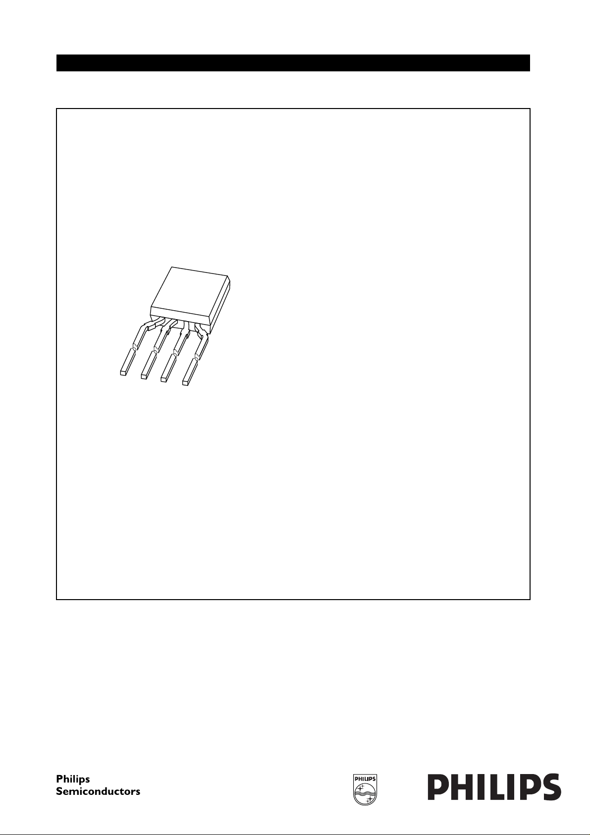
handbook, halfpage
M3D329
KMZ10A1
Magnetic field sensor
Product specification
Supersedes data of 1996 Nov 14
File under Discrete Semiconductors, SC17
1998 Apr 06
Page 2
Philips Semiconductors Product specification
Magnetic field sensor KMZ10A1
DESCRIPTION
The KMZ10A1 is an extremely sensitive magnetic field
sensor, employing the magnetoresistive effect of thin-film
permalloy. Its properties enable this sensor to be used in a
wide range of applications such as navigation, current and
earth magnetic field measurement etc. The special
arrangement of the sensing chip allows the construction of
coils for switching the auxiliary field (Hx) along the length
axis of the sensor. The sensor can be operated at any
frequency between DC and 1 MHz.
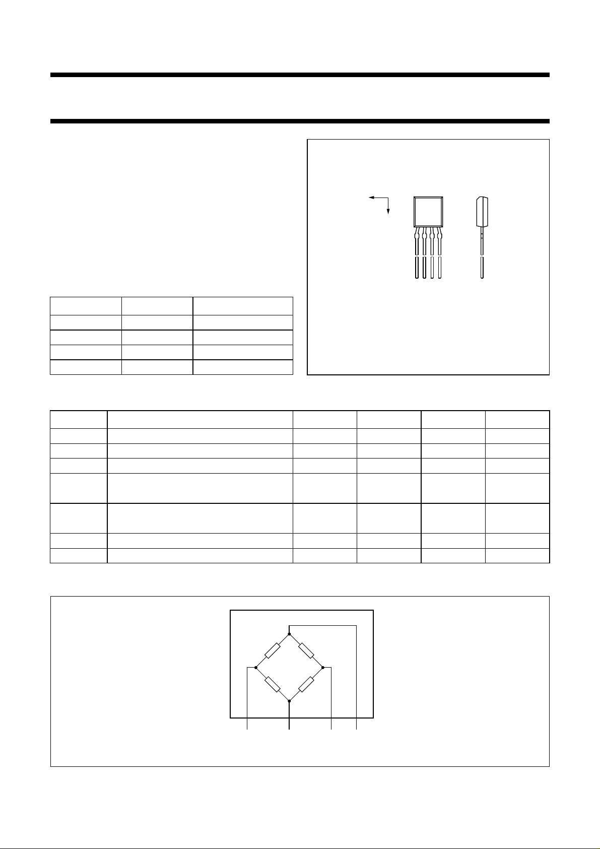
H
handbook, halfpage
y
H
x
PINNING
1234
MGL420
PIN SYMBOL DESCRIPTION
1+V
O
output voltage
2 GND ground
3 −V
4V
O
CC
output voltage
supply voltage
Fig.1 Simplified outline.
QUICK REFERENCE DATA
SYMBOL PARAMETER MIN. TYP. MAX. UNIT
V
CC
H
y
H
x
S sensitivity − 14 −
S
s
R
bridge
V
offset
DC supply voltage − 5 − V
magnetic field strength −0.5 − +0.5 kA/m
auxiliary field − 0.5 − kA/m
mV V⁄
----------------kA m⁄
sensitivity (with switched Hx) − 22 −
mV V⁄
----------------kA m⁄
bridge resistance 0.85 − 1.75 kΩ
offset voltage −1.5 − +1.5 mV/V
CIRCUIT DIAGRAM
handbook, full pagewidth
1
+V
O
GND
Fig.2 Simplified circuit diagram.
1998 Apr 06 2
–V
MLC716
432
V
O
CC
Page 3
Philips Semiconductors Product specification
Magnetic field sensor KMZ10A1
LIMITING VALUES
In accordance with the Absolute Maximum Rating System (IEC 134).
SYMBOL PARAMETER CONDITIONS MIN. MAX. UNIT
V
CC
P
tot
T
stg
T
bridge
DC supply voltage − 9V
total power dissipation up to T
= 132 °C − 100 mW
amb
storage temperature −65 +150 °C
bridge operating temperature −40 +150 °C
150
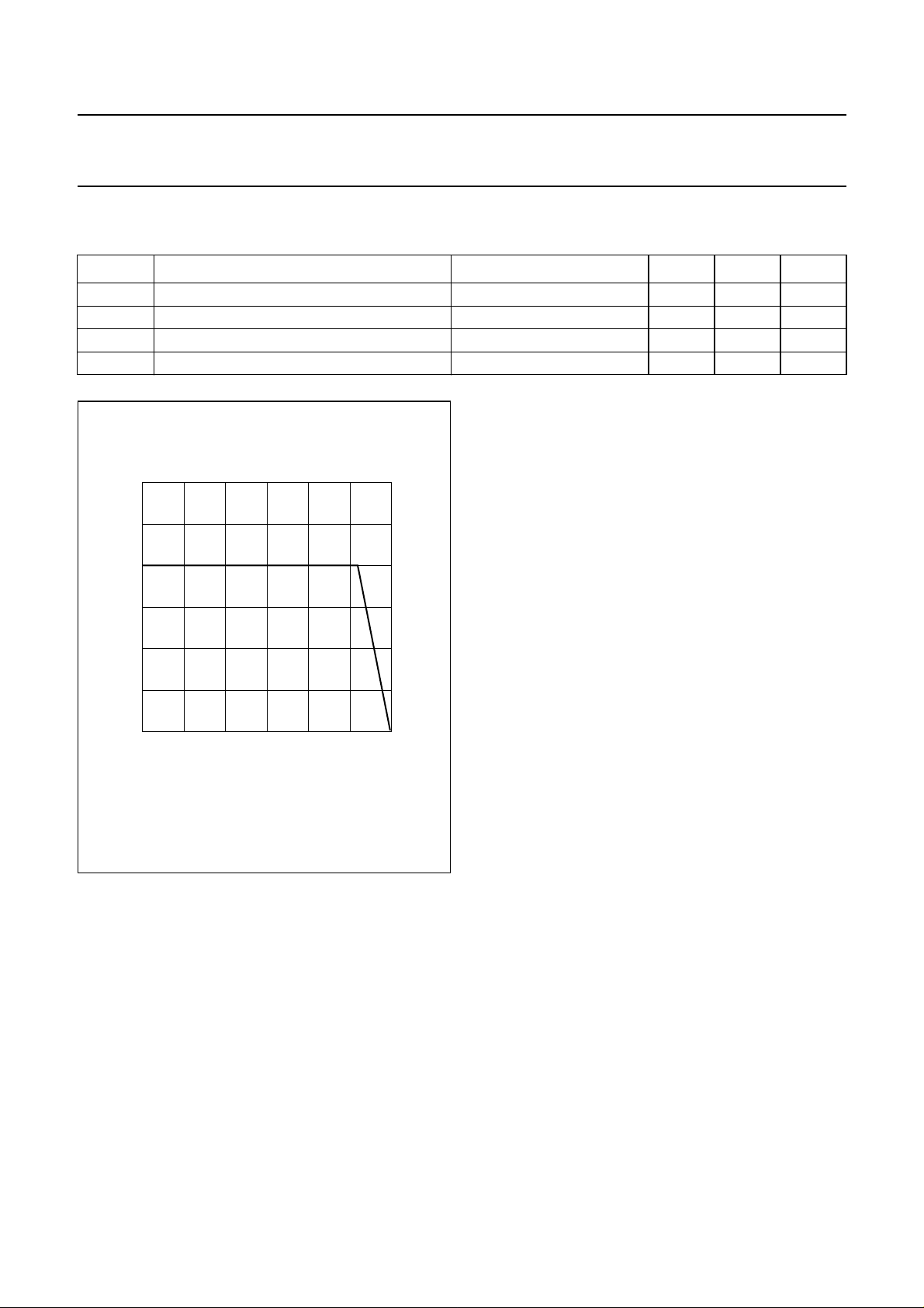
handbook, halfpage
P
tot
(mW)
100
50
0
0
50 100 150
T ( C)
amb
Fig.3 Power derating curve.
MSA927
o
1998 Apr 06 3
Page 4

Philips Semiconductors Product specification
Magnetic field sensor KMZ10A1
THERMAL CHARACTERISTICS
SYMBOL PARAMETER VALUE UNIT
R
th j-a
CHARACTERISTICS
=25°C and Hx= 0.5 kA/m unless otherwise specified; see notes 1 and 2.
T
amb
SYMBOL PARAMETER CONDITIONS MIN. TYP. MAX. UNIT
V
CC
H
y
S sensitivity open circuit;
TCV
O
VCV
O
R
bridge
TCR
bridge
V
offset
TCV
offset
FL linearity deviation of output voltage H
FH hysteresis of output voltage −−0.5 %⋅FS
f operating frequency 0 − 1 MHz
thermal resistance from junction to ambient 180 K/W
DC supply voltage − 5 − V
operating range note 2 −0.5 −+0.5 kA/m
temperature coefficient of output
voltage at constant supply voltage
temperature coefficient of output
voltage at constant supply current
notes 2 and 3
VCC=5V;
T
= −25 to +125 °C
amb
IB= 3 mA;
T
= −25 to +125 °C
amb
11 − 17
−−0.4 − %/K
−−0.15 − %/K
mV V⁄
----------------kA m⁄
bridge resistance 0.85 − 1.75 kΩ
temperature coefficient of bridge
Tj= −25 to +125 °C − 0.25 − %/K
resistance
offset voltage −1.5 − +1.5 mV/V
offset voltage drift T
= −25 to +125 °C −6 −+6
bridge
=0to±0.25 kA/m
y
=0to±0.4 kA/m
H
y
H
=0to±0.5 kA/m
y
−1
−−0.8 %⋅FS
−1
−1
−−2.5 %⋅FS
−−4.0 %⋅FS
µ VV⁄
---------------
K
Characteristics with H
H
S
y
s
operating range note 2 −0.05 −+0.05 kA/m
sensitivity slope between Hy=0
= 0 (switched Hx, see note 4); VCC=5V
x
and Hy= 40 A/m
14 − 27
mV V⁄
----------------kA m⁄
Notes
1. Before first operation or after operation outside the SOAR (Fig.4) the sensor has to be reset by application of an
auxiliary field H
2. No disturbing field (H
= 3 kA/m.
x
) allowed; for stable operation under disturbing conditions see Fig.4 (SOAR) and see Fig.5 for
d
decrease of sensitivity.
3. Sensitivity measured as ∆V
/∆Hy between Hy= 0 and Hy= 0.4 kA/m.
O
4. See application information.
1998 Apr 06 4
Page 5

Philips Semiconductors Product specification
Magnetic field sensor KMZ10A1
SOAR
I
3
Hx (kA/m)
= 3 kA/m.
MGD807
12
handbook, halfpage
H
d
(kA/m)
8
4
0
I =Region of permissible operation.
II = Permissible extension if Hy< 0.05 kA/m.
In applications with Hx< 3 kA/m, the sensor has to be reset, after
leaving the SOAR, by an auxiliary field of H
H
y
H
H
d
x
II
012 4
II
x
Fig.4 Safe Operating Area (permissible disturbing
field Hd as a component of auxiliary field Hx).
handbook, halfpage
1.2
S
(H )
x
S
(0.5 kA/m)
0.8
0.4
0
05
In applications with Hx≤ 3 kA/m, the sensor has to be
reset by an auxiliary field of H
1234
= 3 kA/m before use.
x
H (kA/m)
x
Fig.5 Relative sensitivity (ratio of sensitivity at
certain Hx and sensitivity at Hx= 0.5 kA/m).
MLC120
10
handbook, halfpage
V
O
(mV/V)
6
2
0
–2
–6
–10
–0.5 0.5
Hx= 0.5 kA/m; T
–0.3 –0.1 0.1 0.3
=25°C; V
amb
0
= 0; S = ∆VO/ ∆Hy.
offset
Fig.6 Sensor output characteristics.
∆ H
y
MEA558
Hy (kA/m)
∆ V
1.2
handbook, halfpage
V
O
(mV/V)
0.8
O
0.4
0
–0.4
–0.8
–1.2
–50
(1) Sensor reset with Hx= 3 kA/m.
(2) Sensor reset with Hx= −3 kA/m.
–30 50
–10 10 30
(1)
(2)
0
MEA557
Hy (A/m)
Fig.7 Output characteristic with Hx=0
(switched Hx).
1998 Apr 06 5
Page 6

Philips Semiconductors Product specification
Magnetic field sensor KMZ10A1
APPLICATION INFORMATION
A problem with measuring weak magnetic fields is that precision is limited by drift in both the sensor and amplifier offset.
In these instances, it is possible to take advantage of the ‘flipping’ characteristics of the KMZ10 series to generate an
output that is independent of offset. The sensor, located in a coil connected to a current pulse generator producing
magnetic field pulses periodically reversed by alternate positive and negative going current pulses, is continually flipped
from its normal to its reversed polarity and back again. The polarity of the offset however, remains unchanged, so the
offset itself can be eliminated by passing the output signal through a filter circuit.
handbook, full pagewidth
1234
V
o
H
(a)
sensor
coil
V
o
M
x
offset
M
x
H
y
x
H
y
(c)
polarizationcurrent
offset
time
(b)
MBC925
(a) Set-up.
(b) Pulse diagram.
(c) Sensor output characteristics.
Fig.8 Measuring weak magnetic fields with the KMZ10A1.
1998 Apr 06 6
Page 7

Philips Semiconductors Product specification
Magnetic field sensor KMZ10A1
PACKAGE OUTLINE
Plastic single-ended flat package; 4 in-line leads SOT195
E
Q
b
1
A
D
L
chip
L
1
1234
e
1
e
DIMENSIONS (mm are the original dimensions)
UNIT b
Notes
1. Terminal dimensions within this zone are uncontrolled to allow for flow of plastic and terminal irregularities.
AD
p
0.48
1.8
mm
OUTLINE
VERSION
SOT195 97-06-02
1.6
0.40
c
b
1
0.7
0.45
0.5
0.39
IEC JEDEC EIAJ
5.2
5.0
E
4.8
4.4
REFERENCES
b
p
0 1 4 mm
scale
e
e
3.75
1.25
L
1
14.5
12.7
L
1
max.
2
c
(1)
Q
0.8
0.7
EUROPEAN
PROJECTION
ISSUE DATE
1998 Apr 06 7
Page 8

Philips Semiconductors Product specification
Magnetic field sensor KMZ10A1
DEFINITIONS
Data Sheet Status
Objective specification This data sheet contains target or goal specifications for product development.
Preliminary specification This data sheet contains preliminary data; supplementary data may be published later.
Product specification This data sheet contains final product specifications.
Limiting values
Limiting values given are in accordance with the Absolute Maximum Rating System (IEC 134). Stress above one or
more of the limiting values may cause permanent damage to the device. These are stress ratings only and operation
of the device at these or at any other conditions above those given in the Characteristics sections of the specification
is not implied. Exposure to limiting values for extended periods may affect device reliability.
Application information
Where application information is given, it is advisory and does not form part of the specification.
LIFE SUPPORT APPLICATIONS
These products are not designed for use in life support appliances, devices, or systems where malfunction of these
products can reasonably be expected to result in personal injury. Philips customers using or selling these products for
use in such applications do so at their own risk and agree to fully indemnify Philips for any damages resulting from such
improper use or sale.
1998 Apr 06 8
Page 9

Philips Semiconductors Product specification
Magnetic field sensor KMZ10A1
NOTES
1998 Apr 06 9
Page 10

Philips Semiconductors Product specification
Magnetic field sensor KMZ10A1
NOTES
1998 Apr 06 10
Page 11

Philips Semiconductors Product specification
Magnetic field sensor KMZ10A1
NOTES
1998 Apr 06 11
Page 12

Philips Semiconductors – a worldwide company
Argentina: see South America
Australia: 34 Waterloo Road, NORTH RYDE, NSW 2113,
Tel. +61 2 9805 4455, Fax. +61 29805 4466
Austria: Computerstr. 6, A-1101 WIEN, P.O. Box 213, Tel. +43 160 1010,
Fax. +43 160 101 1210
Belarus: Hotel Minsk Business Center, Bld. 3, r. 1211, Volodarski Str. 6,
220050 MINSK, Tel. +375 172 200 733, Fax. +375 172 200773
Belgium: see The Netherlands
Brazil: seeSouth America
Bulgaria: Philips Bulgaria Ltd., Energoproject, 15thfloor,
51 James Bourchier Blvd., 1407 SOFIA,
Tel. +359 2 689 211, Fax. +359 2689 102
Canada: PHILIPS SEMICONDUCTORS/COMPONENTS,
Tel. +1 800 234 7381
China/Hong Kong: 501 Hong Kong Industrial Technology Centre,
72 Tat Chee Avenue, Kowloon Tong, HONG KONG,
Tel. +852 2319 7888, Fax. +8522319 7700
Colombia: see South America
Czech Republic: see Austria
Denmark: Prags Boulevard 80, PB 1919, DK-2300 COPENHAGEN S,
Tel. +45 32 88 2636, Fax. +45 31 57 0044
Finland: Sinikalliontie 3, FIN-02630 ESPOO,
Tel. +358 9 615800, Fax. +358 9 61580920
France: 51 Rue Carnot, BP317, 92156 SURESNES Cedex,
Tel. +33 1 40 99 6161, Fax. +33 1 4099 6427
Germany: Hammerbrookstraße 69, D-20097 HAMBURG,
Tel. +49 40 23 53 60, Fax. +4940 23536 300
Greece: No. 15, 25th March Street, GR 17778 TAVROS/ATHENS,
Tel. +30 1 4894 339/239, Fax. +30 14814 240
Hungary: seeAustria
India: Philips INDIA Ltd, Band Box Building, 2nd floor,
254-D, Dr. Annie BesantRoad, Worli, MUMBAI 400 025,
Tel. +91 22 493 8541, Fax.+91 22493 0966
Indonesia: PT Philips Development Corporation, Semiconductors Division,
Gedung Philips, Jl. Buncit Raya Kav.99-100, JAKARTA 12510,
Tel. +62 21 794 0040 ext.2501, Fax. +6221 7940080
Ireland: Newstead, Clonskeagh, DUBLIN 14,
Tel. +353 1 7640 000, Fax.+353 17640 200
Israel: RAPAC Electronics, 7 Kehilat Saloniki St, PO Box 18053,
TEL AVIV 61180, Tel. +972 3 645 0444, Fax.+972 3649 1007
Italy: PHILIPS SEMICONDUCTORS, Piazza IV Novembre 3,
20124 MILANO, Tel. +39 2 6752 2531, Fax. +39 2 6752 2557
Japan: Philips Bldg 13-37, Kohnan 2-chome, Minato-ku, TOKYO 108,
Tel. +81 3 3740 5130, Fax. +81 33740 5077
Korea: Philips House, 260-199 Itaewon-dong, Yongsan-ku, SEOUL,
Tel. +82 2 709 1412, Fax. +82 2 709 1415
Malaysia: No. 76 Jalan Universiti, 46200 PETALING JAYA, SELANGOR,
Tel. +60 3 750 5214, Fax. +60 3 7574880
Mexico: 5900 Gateway East, Suite 200, EL PASO, TEXAS 79905,
Tel. +9-5 800 234 7381
Middle East: see Italy
Netherlands: Postbus 90050, 5600 PB EINDHOVEN, Bldg. VB,
Tel. +31 40 27 82785, Fax. +31 4027 88399
New Zealand: 2 Wagener Place, C.P.O. Box 1041, AUCKLAND,
Tel. +64 9 849 4160, Fax. +64 9 849 7811
Norway: Box 1, Manglerud 0612, OSLO,
Tel. +47 22 74 8000, Fax. +47 22 74 8341
Pakistan: see Singapore
Philippines: Philips Semiconductors Philippines Inc.,
106 Valero St. Salcedo Village, P.O. Box 2108 MCC,MAKATI,
Metro MANILA, Tel. +63 2 816 6380, Fax. +632 817 3474
Poland: Ul. Lukiska 10, PL 04-123 WARSZAWA,
Tel. +48 22 612 2831, Fax.+48 22612 2327
Portugal: see Spain
Romania: see Italy
Russia: Philips Russia, Ul. Usatcheva 35A, 119048 MOSCOW,
Tel. +7 095 755 6918, Fax.+7 095755 6919
Singapore: Lorong 1, Toa Payoh, SINGAPORE 319762,
Tel. +65 350 2538, Fax. +65 251 6500
Slovakia: see Austria
Slovenia: see Italy
South Africa: S.A. PHILIPS Pty Ltd., 195-215 Main Road Martindale,
2092 JOHANNESBURG, P.O. Box 7430 Johannesburg 2000,
Tel. +27 11 470 5911, Fax.+27 11470 5494
South America: Al. Vicente Pinzon, 173, 6th floor,
04547-130 SÃO PAULO, SP, Brazil,
Tel. +55 11 821 2333, Fax.+55 11821 2382
Spain: Balmes 22, 08007 BARCELONA,
Tel. +34 3 301 6312, Fax. +34 3 301 4107
Sweden: Kottbygatan 7, Akalla, S-16485 STOCKHOLM,
Tel. +46 8 5985 2000, Fax. +46 85985 2745
Switzerland: Allmendstrasse 140, CH-8027 ZÜRICH,
Tel. +41 1 488 2741 Fax. +41 1 488 3263
Taiwan: Philips Semiconductors, 6F, No. 96, Chien Kuo N. Rd., Sec. 1,
TAIPEI, Taiwan Tel. +886 2 2134 2865, Fax. +886 2 2134 2874
Thailand: PHILIPS ELECTRONICS (THAILAND) Ltd.,
209/2 Sanpavuth-Bangna Road Prakanong, BANGKOK 10260,
Tel. +66 2 745 4090, Fax. +66 2 398 0793
Turkey: Talatpasa Cad. No. 5, 80640 GÜLTEPE/ISTANBUL,
Tel. +90 212 279 2770, Fax. +90 212 282 6707
Ukraine: PHILIPS UKRAINE, 4 Patrice Lumumba str., Building B, Floor 7,
252042 KIEV, Tel. +380 44 264 2776, Fax. +38044 268 0461
United Kingdom: Philips Semiconductors Ltd., 276 Bath Road, Hayes,
MIDDLESEX UB3 5BX, Tel. +44 181 730 5000, Fax.+44 181754 8421
United States: 811 East Arques Avenue, SUNNYVALE, CA 94088-3409,
Tel. +1 800 234 7381
Uruguay: see South America
Vietnam: see Singapore
Yugoslavia: PHILIPS, Trg N. Pasica 5/v, 11000 BEOGRAD,
Tel. +381 11 625 344, Fax.+38111 635777
For all other countries apply to: Philips Semiconductors,
International Marketing & Sales Communications, Building BE-p, P.O. Box 218,
5600 MD EINDHOVEN, The Netherlands, Fax. +31 40 27 24825
© Philips Electronics N.V. 1998 SCA59
All rights are reserved. Reproduction in whole or in part is prohibited without the prior written consent of the copyright owner.
The information presented in this document does not form part of any quotation or contract, is believed to be accurate and reliable and may be changed
without notice. No liability will be accepted by the publisher for any consequence of its use. Publication thereof does not convey nor imply any license
under patent- or other industrial or intellectual property rights.
Internet: http://www.semiconductors.philips.com
Printed in The Netherlands 115106/00/03/pp12 Date of release: 1998 Apr 06 Document order number: 9397 750 03712
 Loading...