

Page 1
www.fairchildsemi.com
KA78MXX
3-Term inal 0.5A Positive Voltage Regulator
Features
• Output Current up to 0.5A
• Output Voltages of 5, 6, 8, 12, 15, 18, 24V
• Thermal Overload Protection
• Short Circuit Protection
• Output Transistor Safe Operat ing Area (SOA) Protection
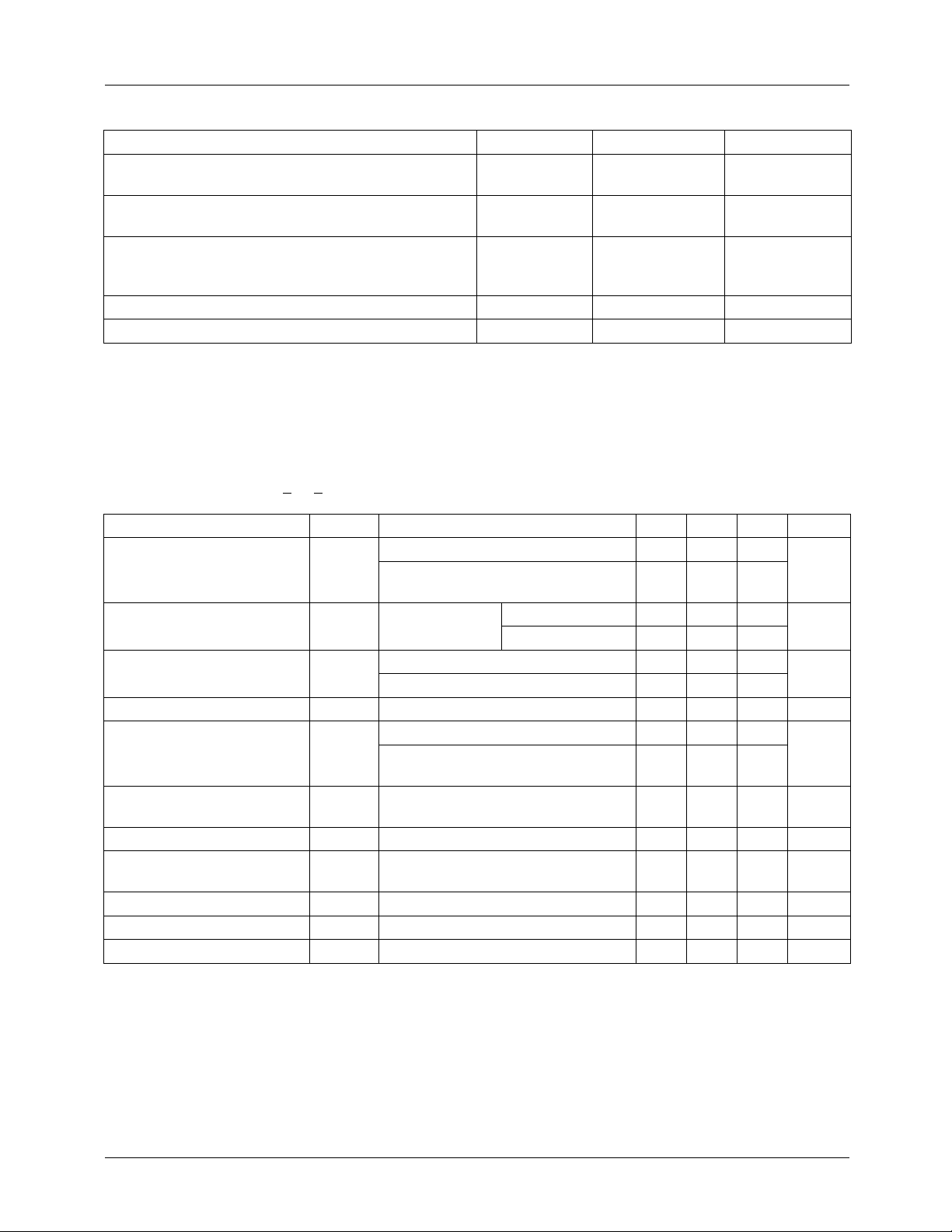
Internal Block Diagram
Description
The KA78MXX series of three terminal positive regulators
are available in the TO-220/D-PAK package with several
fixed output voltages making it useful in a wide range of
applications.
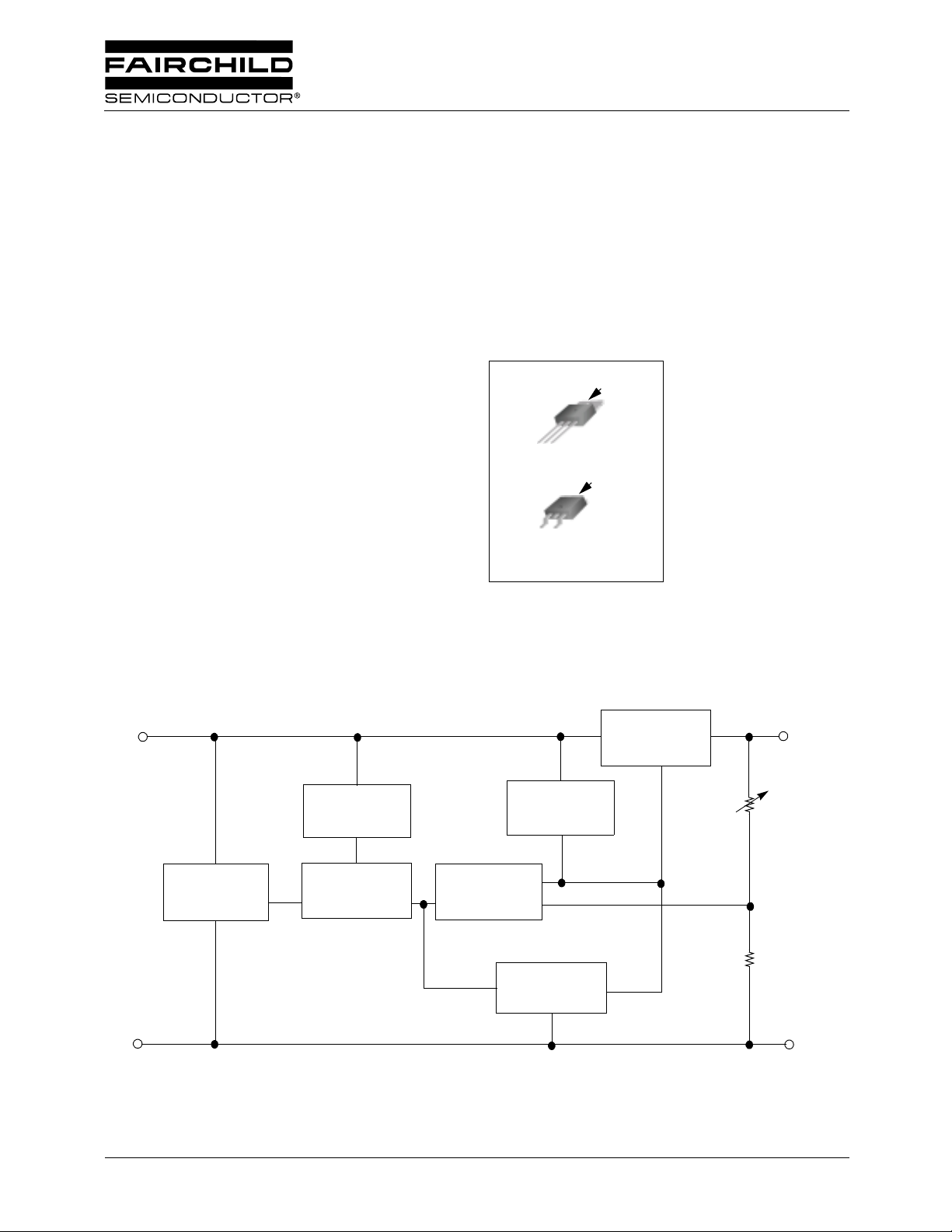
TO-220
1
D-PAK
1
1. Input 2. GND 3. Output
GND
GND
INPUT
1
CURRENT
GENERATOR
STARTING
CIRCUIT
©2002 Fairchild Semiconductor Corporation
REFERENCE
VOLTAGE
ERROR
AMPLIFIER
SOA
PROTECTION
THERMAL
PROTECTION
SERIES
PASS
ELEMENT
OUTPUT
3
R1
R2
GND
2
Rev. 1.0.5
Page 2
KA78MXX
Absolute Maximum Ratings
Parameter Symbol Value Unit
Input Voltage (for V
(for V
= 24V)
O
Thermal Resistance Junction-Cases (Note1)
TO-220 (Tc = +25°C)
= 5V to 18V)
O
R
V
I
V
I
θJC
35
40
2.5 °C/W
Thermal Resistance Junction-Air (Note1,2)
TO-220 (Ta = +25°C)
D-PAK (Ta = +25°C)
Operating Junction Temperature Range T
Storage Temperature Range T
Note:
1. Thermal resistance test board
Size: 76.2mm * 114.3mm * 1.6mm(1S0P)
JEDEC standard: JESD51 -3, JESD51-7
2. Assume no ambient airflow
R
θJA
OPR
STG
66
°C/W
92
0 ~ +150 °C
-65 ~ +150 °C
Electrical Characteristics (KA78M05/KA78M05R)
(Refer to the test circuits, 0
< TJ < +125°C, IO=350mA, VI=10V, unless otherwise specified, CI =0.33µF, CO=0.1µF)
V
V
Parameter Symbol Conditions Min. Typ. Max. Unit
TJ =+25°C4.855.2
Output Voltage V
Line Regulation (Note3) ∆V
Load Regulation (Note3) ∆V
Quiescent Current I
O
O
= 5 to 350mA
I
O
V
= 7 to 20V
I
IO = 200mA
T
=+25°C
J
4.75 5 5.25
V
= 7 to 25V - - 100
I
= 8 to 25V - - 50
V
I
IO = 5mA to 0.5A, TJ = +25°C - - 100
O
Q
= 5mA to 200mA, TJ =+25°C--50
I
O
TJ = +25°C-4.06.0mA
V
mV
mV
IO = 5mA to 350mA - - 0.5
Quiescent Current Change ∆I
Q
Output Voltage Drift ∆V/∆T
Output Noise Voltage V
N
Ripple Rejection RR
Dropout Voltage V
Short Circuit Current I
Peak Current I
D
SC
PK
= 200mA
I
O
V
= 8 to 25V
I
= 5mA
I
O
T
= 0 to +125°C
J
--0.8
--0.5-mV/°C
f = 10Hz to 100kHz - 40 f = 120Hz, I
V
= 8 to 18V, TJ = +25°C
I
= 300mA
O
-80- dB
TJ = +25°C, IO = 500mA - 2 - V
TJ = +25°C, VI = 35V - 300 - mA
TJ = +25°C - 700 - mA
mA
µ
V/Vo
Note:
3. Load and line regulation are specified at constant junction temperature. Change in V
into account separately. Pulse testing with low duty is used.
2
due to heating effects must be taken
o
Page 3

KA78MXX
Electrical Characteristics (KA78M06/KA78M06R)
(Continued)
(Refer to the test circuits, 0 < TJ < +125°C, IO=350mA, VI=11V, unless otherwise specified, CI =0.33µF, CO=0.1µF)
Parameter Symbol Conditions Min. Typ. Max. Unit
TJ = +25°C 5.75 6 6.25
Output Voltage V
Line Regulation (Note1) ∆V
Load Regulation (Note1) ∆V
Quiescent Current I
O
O
= 5 to 350mA
I
O
V
= 8 to 21V
I
IO = 200mA
T
=+25°C
J
5.7 6 6.3
V
= 8 to 25V - - 100
I
= 9 to 25V - - 50
V
I
IO = 5mA to 0.5A, TJ =+25°C - - 120
O
Q
= 5mA to 200mA, TJ =+25°C--60
I
O
TJ =+25°C-4.06.0mA
V
mV
mV
IO = 5mA to 350mA - - 0.5
Quiescent Current Change ∆I
Q
Output Voltage Drift ∆V/∆T
Output Noise Voltage V
N
Ripple Rejection RR
Dropout Voltage V
Short Circuit Current I
Peak Current I
D
SC
PK
= 200mA
I
O
V
= 9 to 25V
I
I
= 5mA
O
T
= 0 to +125°C
J
--0.8
--0.5-mV/°C
f = 10Hz to 100kHz - 45 f = 120Hz, I
V
= 9 to 19V, TJ = +25°C
I
= 300mA
O
-80- dB
TJ =+25°C, IO = 500mA - 2 - V
TJ= +25°C, VI = 35V - 300 - mA
TJ =+25°C - 700 - mA
mA
µ
V/Vo
Note:
1. Load and line regulation are specified at constant, junction temperature. Change in V
into account separately. Pulse testing with low duty is used.
due to heating effects must be taken
o
3
Page 4
KA78MXX
Electrical Characteristics (KA78M08/KA78M08R)
(Continued)
(Refer to the test circuits, 0 < TJ < +125°C, IO=350mA, VI=14V, unless otherwise specified, CI =0.33µF, CO=0.1µF)
Parameter Symbol Conditions Min. Typ. Max. Unit
TJ = +25°C 7.7 8 8.3
Output Voltage V
Line Regulation (Note1) ∆V
Load Regulation (Note1) ∆V
Quiescent Current I
O
O
= 5 to 350mA
I
O
V
= 10.5 to 23V
I
IO = 200mA
T
=+25°C
J
7.6 8 8.4
V
= 10.5 to 25V - - 100
I
= 11 to 25V - - 50
V
I
IO = 5mA to 0.5A, TJ = +25°C - - 160
O
Q
= 5mA to 200mA, TJ = +25°C--80
I
O
TJ = +25°C-4.06.0mA
V
mV
mV
IO = 5mA to 350mA - - 0.5
Quiescent Current Change ∆I
Output Voltage Drift RR
Output Noise Voltage V
Ripple Rejection RR
Dropout Voltage V
Short Circuit Current I
Peak Current I
SC
PK
Q
N
D
= 200mA
I
O
V
= 10.5 to 25V
I
I
= 5mA
O
T
= 0 to +125°C
J
--0.8
--0.5-mV/°C
f = 10Hz to 100kHz - 52 f = 120Hz, I
V
= 11.5 to 21.5V, TJ = +25°C
I
= 300mA
O
-80-dB
TJ =+25°C, IO = 500mA - 2 - V
TJ =+25°C, VI= 35V - 300 - mA
TJ =+25°C - 700 - mA
mA
µ
V/Vo
Note:
1. Load and line regulation are specified at constant, junction temperature. Change in V
into account separately. Pulse testing with low duty is used.
due to heating effects must be taken
o
4
Page 5
KA78MXX
Electrical Characteristics (KA78M12/KA78M12R)
(Continued)
(Refer to the test circuits, 0 < TJ < +125°C, IO=350mA, VI=19V, unless otherwise specified, CI =0.33µF, CO=0.1µF)
Parameter Symbol Conditions Min. Typ. Max. Unit
TJ = +25°C 11.5 12 12.5
Output Voltage V
Line Regulation (Note1) ∆V
Load Regulation (Note1) ∆V
Quiescent Current I
O
O
= 5 to 350mA
I
O
V
= 14.5 to 27V
I
IO = 200mA
T
= +25°C
J
11.4 12 12.6
V
= 14.5 to 30V - - 100
I
= 16 to 30V - - 50
V
I
IO = 5mA to 0.5A, TJ = +25°C - - 240
O
Q
= 5mA to 200mA, TJ =+25°C - - 120
I
O
TJ=+25°C-4.16.0mA
V
mV
mV
IO = 5mA to 350mA - - 0.5
Quiescent Current Change ∆I
Q
Output Voltage Drift ∆V/∆T
Output Noise Voltage V
N
Ripple Rejection RR
Dropout Voltage V
Short Circuit Current I
Peak Current I
D
SC
PK
= 200mA
I
O
V
= 14.5 to 30V
I
I
= 5mA
O
T
= 0 to +125°C
J
--0.8
--0.5-mV/°C
f = 10Hz to 100kHz - 75 f = 120Hz, I
V
= 15 to 25V, TJ = +25°C
I
= 300mA
O
-80-dB
TJ =+25°C, IO = 500mA - 2 - V
TJ= +25°C, VI = 35V - 300 - mA
TJ = +25°C - 700 - mA
mA
µ
V/Vo
Note:
1. Load and line regulation are specified at constant, junction temperature. Change in V
into account separately. Pulse testing with low duty is used.
due to heating effects must be taken
o
5
Page 6

KA78MXX
Electrical Characteristics (KA78M15)
(Continued)
(Refer to the test circuits, 0 < TJ < +125°C, IO=350mA, VI=23V, unless otherwise specified, CI =0.33µF, CO=0.1µF)
Parameter Symbol Conditions Min. Typ. Max. Unit
TJ =+25°C 14.4 15 15.6
Output Voltage V
Line Regulation (Note1) ∆V
Load Regulation (Note1) ∆V
Quiescent Current I
O
O
= 5 to 350mA
I
O
V
= 17.5 to 30V
I
IO = 200mA
T
= +25°C
J
14.25 15 15.75
V
= 17.5 to 30V - - 100
I
= 20 to 30V - - 50
V
I
IO = 5mA to 0.5A, TJ =+25°C - - 300
O
Q
= 5mA to 200mA, TJ =+25°C - - 150
I
O
TJ =+25°C-4.16.0mA
V
mV
mV
IO = 5mA to 350mA - - 0.5
Quiescent Current Change ∆I
Q
Output Voltage Drift ∆V/∆T
Output Noise Voltage V
N
Ripple Rejection RR
Dropout Voltage V
Short Circuit Current I
Peak Current I
D
SC
PK
= 200mA
I
O
V
= 17.5 to 30V
I
I
= 5mA
O
T
= 0 to +125°C
J
--0.8
--1 -mV/°C
f = 10Hz to 100kHz - 100 f = 120Hz, I
V
= 18.5 to 28.5V, TJ = +25°C
I
= 300mA
O
-70 - dB
TJ =+25°C, IO = 500mA - 2 - V
TJ= +25°C, VI = 35V - 300 - mA
TJ = +25°C - 700 - mA
mA
µ
V/Vo
Note:
1. Load and line regulation are specified at constant, junction temperature. Change in V
into account separately. Pulse testing with low duty is used.
due to heating effects must be taken
o
6
Page 7

KA78MXX
Electrical Characteristics (KA78M18)
(Continued)
(Refer to the test circuits, 0 < TJ < +125°C, IO=350mA, VI=26V, unless otherwise specified, CI =0.33µF, CO=0.1µF)
Parameter Symbol Conditions Min. Typ. Max. Unit
TJ = +25°C 17.3 18 18.7
Output Voltage V
O
Line Regulation (Note1) ∆V
Load Regulation (Note1) ∆VΟ
Quiescent Current I
Q
= 5 to 350mA
I
O
O
V
= 20.5 to 33V
I
V
= 21 to 33V - - 100
IO = 200mA
T
=+25°C
J
= 5mA to 0.5A, TJ = +25°C - - 360
I
O
= 5mA to 200mA, TJ = +25°C - - 180
I
O
I
= 24 to 33V - - 50
V
I
17.1 18 18.9
TJ =+25°C-4.26.0mA
V
mV
mV
IO = 5mA to 350mA - - 0.5
Quiescent Current Change ∆I
Output Voltage Drift ∆V/∆TI
Output Noise Voltage V
Ripple Rejection RR
Dropout Voltage V
Short Circuit Current I
Peak Current I
SC
PK
Q
N
= 200mA
I
O
V
= 21 to 33V
I
= 5mATJ = 0 to 125°C--1.1-mV/°C
O
f = 10Hz to 100kHz - 100 - µV/Vo
f = 120Hz, I
T
= +25°C
J
D
TJ = +25°C, IO=500mA - 2 - V
TJ = +25°C, VI=35V - 300 - mA
TJ = +25°C - 700 - mA
=300mA , VI=22 to 32V
O
--0.8
-70 - dB
mA
Note:
1. Load and line regulation are specified at constant, junction temperature. Change in V
into account separately. Pulse testing with low duty is used.
due to heating effects must be taken
o
7
Page 8

KA78MXX
Electrical Characteristics (KA78M24)
(Continued)
(Refer to the test circuits, 0 < TJ < +125°C, IO=350mA, VI=33V, unless otherwise specified, CI =0.33µF, CO=0.1µF)
Parameter Symbol Conditions Min. Typ. Max. Unit
TJ = +25°C232425
Output Voltage V
Line Regulation ∆V
Load Regulation ∆V
Quiescent Current I
O
O
= 5 to 350mA
I
O
V
= 27 to 38V
I
IO = 200mA
T
= +25°C
J
22.8 24 25.2
V
= 27 to 38V - - 100
I
= 28 to 38V - - 50
V
I
IO = 5mA to 0.5A, TJ =+25°C - - 480
O
Q
= 5mA to 200mA, TJ =+25°C - - 240
I
O
TJ = +25°C-4.26mA
V
mV
mV
IO = 5mA to 350mA - - 0.5
Quiescent Current Change ∆I
Q
Output Voltage Drift ∆V/∆T
Output Noise Voltage V
N
Ripple Rejection RR
Dropout Voltage V
Short Circuit Current I
Peak Current I
D
SC
PK
= 200mA
I
O
V
= 27 to 38V
I
I
= 5mA
O
T
= 0 to +125°C
J
--0.8
--1.2-mV/°C
f = 10Hz to 100kHz - 170 f = 120Hz, I
V
= 28 to 38V, TJ = +25°C
I
= 300mA
O
-70- dB
TJ =+25°C, IO = 500mA - 2 - V
TJ = +25 °C, VI = 35V - 300 - mA
TJ = +25°C - 700 - mA
mA
µ
V
Note:
1. Load and line regulation are specified at constant, junction temperature. Change in V
into account separately. Pulse testing with low duty is used.
due to heating effects must be taken
o
8
Page 9

Typical Applications
KA78MXX
3
C
O
0.1µF
V
O
0.3µF
1
KA78MXX
2
V
I
C
I
Figure 1. Fixed Output Regulator
3
C
O
0.1µF
VXX
I
O
R
1
IO =
1
0.33µF
Vxx
R
1
+I
O
KA78MXX
2
I
O
V
I
C
I
Figure 2. Constant Current Regulator
Notes:
1. To specify an output voltage, substitute voltage value for "XX"
2. Although no output capacitor is needed for stability, it does improve transient response.
3. Required if regulator is located an appreciable distance from power Supply filter
V
I
C
I
1
KA78MXX
2
0.33µF
I
O
IR1 ≥ 5I
O
VO = VXX (1+R2/R1) +IOR
3
C
O
0.1µF
V
XX
R
1
R
2
2
Figure 3. Circuit for Increasing Outp ut Voltage
V
O
9
Page 10

KA78MXX
13V < VI < 25V
V
I
-7 < -VI
V
I
0.33µF
< 17V
C1
1
KA78M05
C
I
0.33µF
2
3
2
7
6
LM741
4
3
Figure 4. Adjustable Output Regulator (7 to 30V)
1
KA78M05
2
3
R4
VXX
910Ω
R5
9.1kΩ
6
7
LM741
4
V
O
0.1µF
C
O
10kΩ
V
O
_
2
R3
3
+
R1
10kΩ
C2
0.1µF
VO = Vxx
R
4
R
1
10
Figure 5. 0.5 to 10V Regulator
Page 11

Mechanical Dimensions
Package
9.90
±0.20
(8.70)
(1.70)
±0.20
9.20
±0.10
1.30
(1.46)
ø3.60
±0.10
TO-220
±0.10
2.80
(3.70)(3.00)
±0.20
15.90
(45°)
18.95MAX.
Dimensions in millimeters
4.50
±0.20
+0.10
1.30
–0.05
KA78MXX
±0.20
13.08
[2.54
(1.00)
1.27
±0.10
2.54TYP
±0.20
]
10.00
±0.20
1.52
±0.10
0.80
±0.10
2.54TYP
[2.54
±0.20
±0.30
10.08
+0.10
0.50
–0.05
2.40
±0.20
]
11
Page 12

KA78MXX
Mechanical Dimensions
Package
6.60
±0.20
5.34
±0.30
(4.34)(0.50) (0.50)
±0.20
0.60
±0.20
0.80
(Continued)
D-PAK
±0.20
2.70
±0.20
0.70
±0.20
6.10
±0.30
9.50
Dimensions in millimeters
2.30
±0.10
0.50
±0.10
±0.10
0.91
MIN0.55
MAX0.96
2.30TYP
[2.30±0.20]
0.76
±0.10
2.30TYP
[2.30±0.20]
±0.30
9.50
±0.20
6.10
±0.20
2.70
±0.10
0.89
6.60
±0.20
(5.34)
(5.04)
(1.50)
(2XR0.25)
(0.70)
0.76
0.50
1.02
2.30
(0.90)
(0.10) (3.05)
±0.10
±0.10
±0.20
±0.20
(1.00)
12
Page 13

Ordering Information
Product Number Package Operating Temperature
KA78M05
KA78M06
KA78M08
KA78M12
KA78M15
KA78M18
KA78M24
KA78M05R
KA78M06R
KA78M08R
KA78M12R
TO-220
0 ~ +125°C
D-PAK
KA78MXX
13
Page 14

KA78MXX
DISCLAIMER
FAIRCHILD SEMICONDUCTOR RESERVES THE RIGHT TO MAKE CHANGES WITHOUT FURT HER NOTICE TO ANY
PRODUCTS HEREI N TO IMPROVE RELIABILITY, FUNCTIO N OR DESIGN. FAIRCH IL D DOES NOT ASSUME ANY
LIABILITY ARISING OUT OF THE APPLICATION OR USE OF ANY PRODUCT OR CIRCUIT DESCRIBED HEREIN; NEITHER
DOES IT CONVEY ANY LICENSE UNDER IT S PATENT RIGHTS, NOR THE RIGHTS OF OTHE RS.
LIFE SUPPORT POL I CY
FAIRCHILD’S PR ODUCTS ARE NOT AUTH ORIZED FOR USE AS C RITICAL COMPONENT S IN LIFE SUPPORT DE VICES
OR SYSTEMS WITHOUT THE EXPRESS WRITTEN APPROVAL OF THE PRESIDENT OF FAIRCHILD SEMICONDUCTOR
CORPORATION. As used herein :
1. Life support devices or systems are devices or systems
which, (a) are intended for surgical implant into the body,
or (b) support or sustain life, and (c) whose failure to
perform when properly used in accordance with
2. A critical component in any component of a life support
device or sy stem whose fai lure to perform can be
reasonably expec ted to cause the failur e of the life support
device or system, or to affect its safety or effec t iv ene ss .
instructions for use provided in the labeling, can be
reasonably expected to result in a significant injury of the
user.
www.fairchildsemi.com
11/12/02 0.0m 001
2002 Fairchild Semiconductor Corporation
Stock#DSxxxxxxxx
 Loading...