

Page 1
KA7526
Power Factor Correction Controller
www.fairchildsemi.com
Features
• Internal Startup Timer
• Internal R/C filter which eliminates the Need for an
External R/C filter
• Overvoltage Comparator eliminates Runaway Output
Voltage
• Zero Current Detector
• One Quadrant Multiplier
• Trimmed 1.5% Internal Bandgap Re fe rence
• Under Voltage Lock Out with 5V of Hystere si s
• Totem Pole Output with High State Clamp
• Low Startup and Operating Current
• 8-Pin DIP or 8-Pin SOP
Applications
• Electronic Ballast
•SMPS
Descriptions
The KA7526 provides simple a nd high performance active
power factor correction. KA7526 is optimized for electronic
ballast and low power, high density power supplies requiring
a minimum board area, reduced component cou nt an d lo w
power dissipation. Addition of internal R/C filter eliminates
the need for an external R/C filter. Internal clamping of the
error amplifier and multiplier outputs improves turn on overshoot characteristics and current limiting. Special circuitry
has also been added to prevent no load runaway conditions.
The output drive clamping circuit limits overshoot of the
power MOSFET gate drive Independent of suppl y volt a ge ,
so that it greatly enhance the system reliability.
8-DIP
1
8-SOP
©2000 Fairchild Semiconductor International
1
Rev. 5.0
Page 2
KA7526
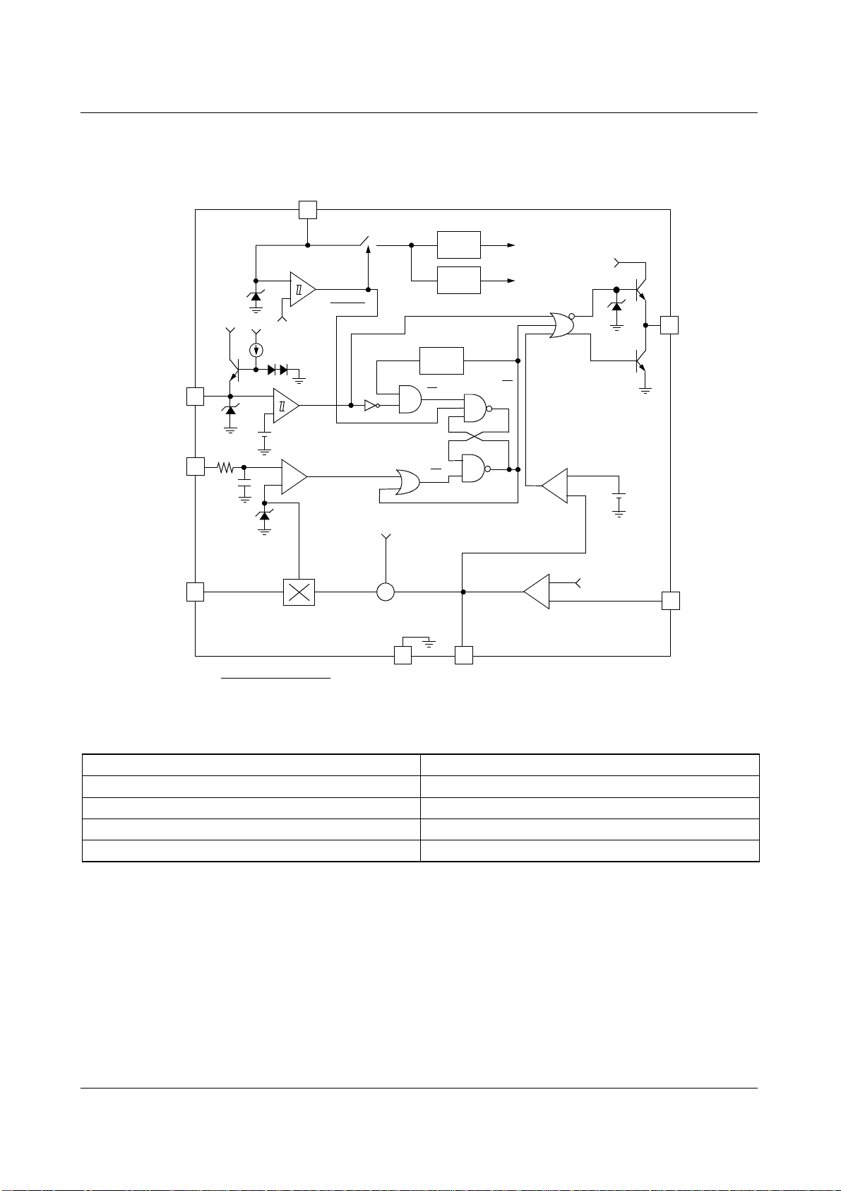
Internal Block Diagram
V
CC
8
Idet
CS
MULT
36V
5
7.5V
1.8V
40k
Ω
4
Vm1
3
0~3.8V
Pin4 Threshold(Vmo)
K =
Vm1
13V
+
-
8pF
1.65V
Vmo
⋅
(Vm2-Vref)
5V
+
-
240mV
Zero Current
Detector
-
+
Current Sense
Comparator
Multiplier
UVLO
Vref
-
GND
2.5V Ref
V
+
-
Error Amp
Vref
CC
Drive
Output
Vea(-)
1.8V
OUT
7
INV
1
Internal
Bias
Timer R
S
R
+
6
2
Q
Vm2
Vref~Vref+2V
EA OUT
Over Voltage
Protection
+
-
IC Characteristics
Parmaeter KA7526
UVLO 8/13V
Multiplier Input Range (Vm1) 0 ~ 3.8V
Multiplier Input Range (Vm2) Vref ~ Verf + 2V
Maximum Current Sense Voltage 1.65V
2
Page 3
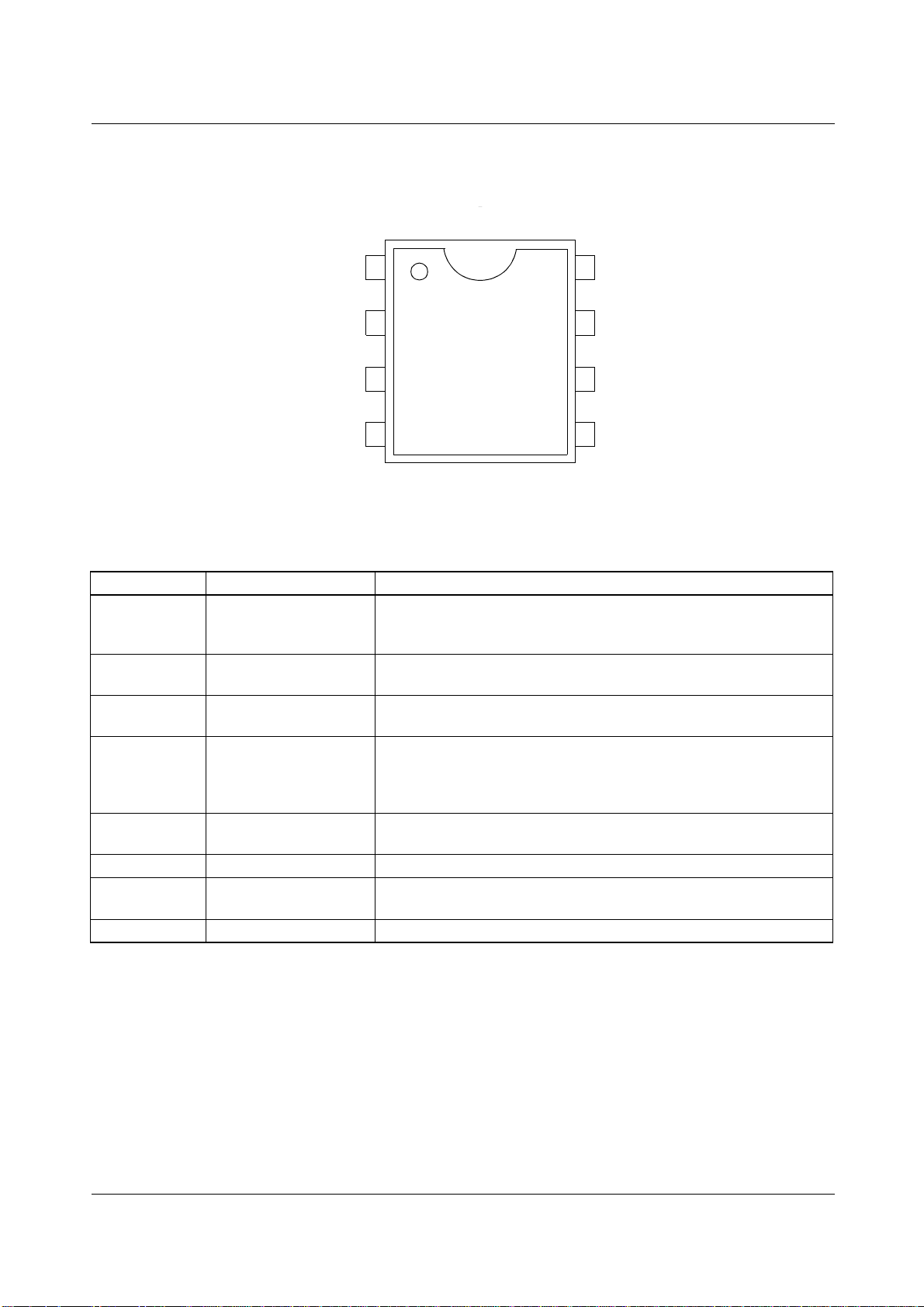
PIN Assignments
KA7526
Vcc
8INV
OUT
7
GND
6
Idet
EA OUT
MULT
CS
1
2
3
45
(Top View)
Pin Definitions
Pin Number Pin Name Pin Function Descrition
Inverting input of the error amplifier. The output of the boost
1 INV
2EA OUT
3MULT
4CS
5 Idet
6 GND The ground potential of all the pins.
7OUT
8V
CC
converter should be resistively divided to 2.5V and con nected to this pin.
The output of the error amplifier. A feedback compensation
network is placed between this pin and the INV pin
Input to the multiplier stage. The full-wave rectified AC is
divided to less than 3.8V and is connected to this pin.
Input to the PWM comparator. The Current is sensed in the boost
stage by a resistor in the source lead of MOSFET. An internal leading
edge blanking circuitry has been included to reject any high
frequency noise present on the current waveform.
The zero current detector senses the inductor current by monitoring
when the boost inductor auxilary winding voltage falls below 1.8V.
The output of a high-current power driver capable of driving
the gate of a power MOSFET.
The logic and control power supply connection.
3
Page 4
KA7526
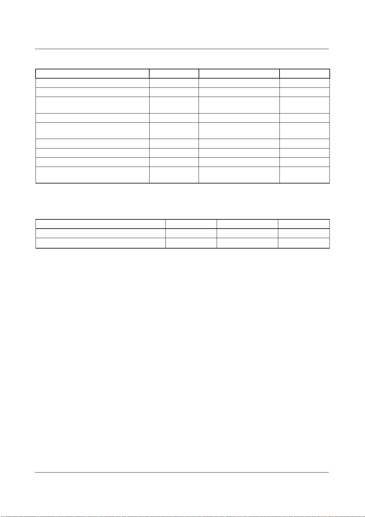
Absolute Maximum Ratings
Parameter Symbol Value Unit
Supply voltage V
Peak drive output current I
Driver output clamping diodes
V
O>VCC
or VO<-0.3V
CC
, I
OH
OI
Iclamp ± 10 mA
Detector clamping diodes Idet ± 3mA
Error amp, multiplier and
comparator input voltage
V
IN
Operating temperature range Topr -25 to 125
Storage temperature range Tstg -65 to 150
Power dissipation
Thermal resistance
(Junction-to-air)
Note :
Based in 8-DIP
(Note)
(Note)
Pd 0.8 W
qja 100
30 V
± 500 mA
-0.3 to 6 V
o
o
o
C
C
C
/W
Temperature Characteristics (-25oC ≤
≤ Ta ≤
≤ 125oC )
≤ ≤
≤ ≤
Parameter Symbol Value Unit
Temperature stability for reference voltage(Vref) ∆Vref (Typ) 20 mV
Temperature stability for multiplier gain(K) ∆K/∆T (Typ)
-0.2
%/
o
C
4
Page 5
KA7526
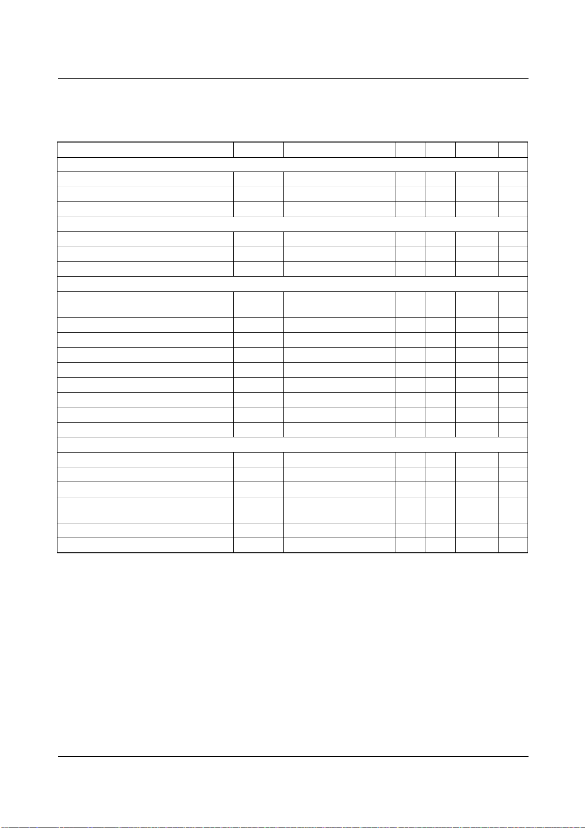
Electrical Characteristics
Unless otherwise specified, for typical values Vcc=12V , Ta=25
with
-25
o
≤ Ta ≤ 125
C
o
.
C
Parameter Symbol Condition Min. Typ. Max. Unit
UNDER VOLTAGE LOCK OUT SECTION
Start Threshold Voltage Vth (st) V
UVLO Hysteresis HY(st) - 4 5 6 V
Supply Zener Voltage Vz I
SUPPLY CURRENT SECTION
Start Up Supply Current Ist V
Operating Supply Current I
CC
Dynamic Operating Supply Current Idcc 50kHz, CI=1nF - 5 10 mA
ERROR AMPLIFIER SECTION
Voltage Feedback Input Threshold Vref
Line Regulation ∆Vref1 12V≤Vcc≤25V - 0.1 10 mV
Load Regulation
Temperature Stability of Vref
(Note1)
(Note2)
∆Vref2 0mA≤Iref≤2mA - 0.1 10 mV
∆Vref3 -25
Input Bias Current Ib(ea) - -0.5 - 0.5 µA
Output Source Current Isource Vm2=3V -2 -4.5 - mA
Output Sink Current Isink Vm2=2V 3 4.5 - mA
Output Voltage Range
(Note2)
∆Veao No Load on E.A Output 1.2 - 5.6 V
Slew Rate SR - - 0.6 - V/µs
MULTIPLIER SECTION
Input Bias Current (pin3) Ib(m) - -0.5 - 0.5 µA
M1 Input Voltage Range (pin3) ∆Vm1 - 0 - 3.8 V
M2 Input Voltage Range (pin2) ∆Vm2 - Vref - Vref+2 V
Multiplier Gain
(Note3)
K
Maximum Multiplier Output Voltage Vomax(m) Vea(-)=0V, Vm1=2V 1.55 1.65 1.75 V
Temperature Stability of K
(Note2)
∆K/∆T-25
o
C, for Min/Max values Ta is the operating ambient tempe rature range
Increasing 12 13 14 V
CC
=10mA 30 36 - V
CC
<Vth(st) - 0.3 0.4 mA
CC
Output not switching - 4 8 mA
Iref=0mA,25
o
C
≤Ta≤125
o
C
≤Ta≤125
o
C
o
C
Vm1=1V,
∆Vm2=2.7 to 3.3V
o
C
≤Ta≤125
o
C
2.44 - 2.56 V
-20 - mV
0.49 0.62 0.74 1/V
--0.2 - %/
o
C
5
Page 6
KA7526
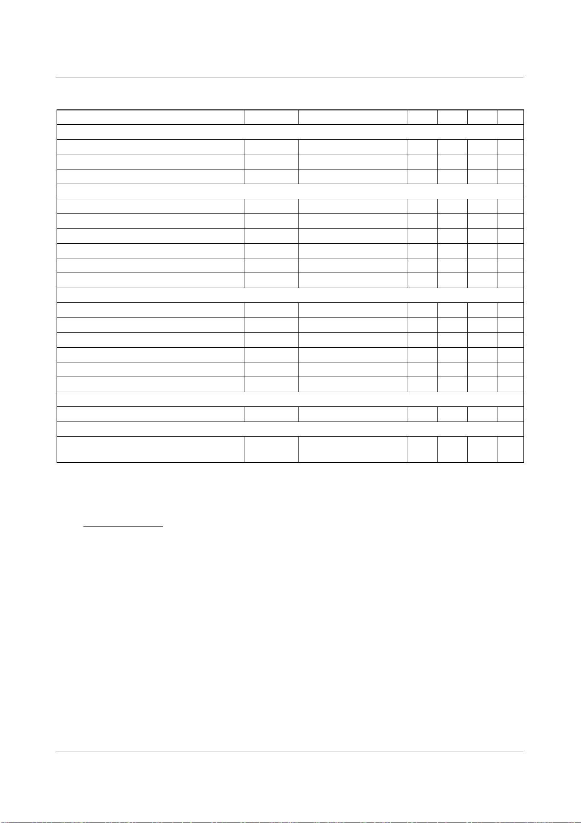
Electrical Characteristics (Continued)
Parameter Symbol Condition Min. Typ. Max. Unit
CURRENT SENSE SECTION
Input Offset Voltage
(Note2)
Input Bias Current Ib(cs) 0V≤V
Current Sense Delay to Output
(Note2)
DETECT SECTION
Detect Input Threshold Vth(det) Vdet Increasing 1.5 1.8 2.1 V
Detect Hysteresis HY(det) - 180 240 400 mV
Input Low Clamp Voltage Vclamp(I) Idet=-100µA 0.45 0.75 1 V
Input High Clamp Voltage Vclamp(h) Idet=3mA 6.7 7.5 8.3 V
Input Bias Current Ib(det) 1V≤Vdet≤6V -1 -0.2 1 µA
Input High/low Clamp Diode Current
(Note2)
OUTPUT DRIVER SECTION
Output Voltage High V
Output Voltage Low V
Rising Time
Falling Time
(Note2)
(Note2)
Maximum Output Voltage Vomax(o) V
Output Voltage With Uvlo Activated Vomin(o) V
RESTART TIMER SECTION
Restart Time Delay td(rst) Vm1=1V, Vm2=3.5V - 300 - µs
OVERVOLTAGE PROTECTION SECTION
Voltage Feedback Input Threshold Vth(ovp)
Notes :
1. Because the reference is not b rou ght out externally, this specification ca nnot be tested on th e p ac kage part. It is guar anteed
by design.
2. This parameter, although guaranteed, is not tested in production.
Vio(cs) Vm1=0V, Vm2=2.2V -10 3 10 mV
≤1.7V -1 -0.3 1 µA
CC
td(cs) - - 200 500 ns
Iclamp - - - ± 3mA
OH
OL
IO=-10mA, VCC=12V 8.5 9 - V
IO=10mA, VCC=12V - 0.8 1 V
tr CI=1nF - 130 200 ns
tf CI=1nF - 50 120 ns
=20V 12 13 15 V
CC
=5V, IO=100µA--1V
CC
Vcs=-0.5V, Vm1=1V
Vdet=0V
1.7 1.8 1.9 V
3. K =
6
Pin4 Threshold
Vm1×(Vm2-Vref)
(Vm1=Vpin3, Vm2=Vpin2)
Page 7
Typica l Perfo rma nce Characteristics
KA7526
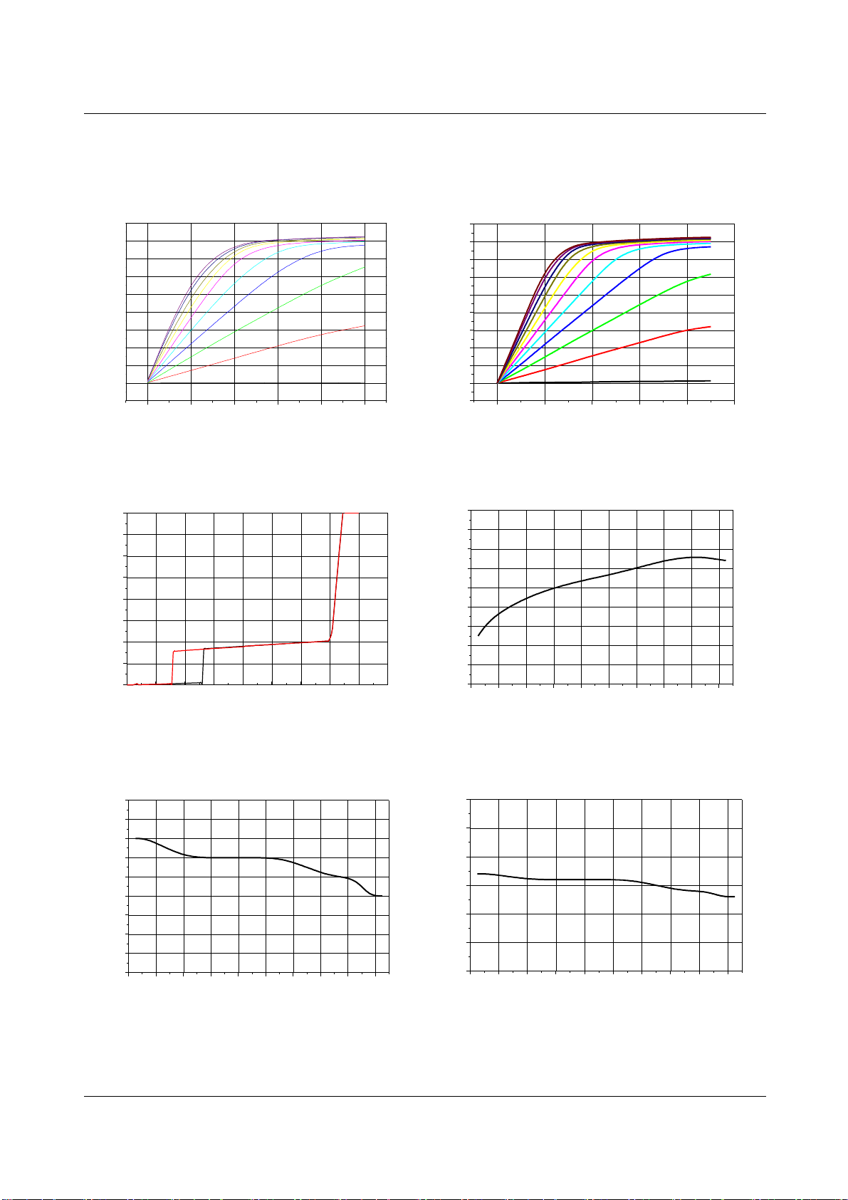
Fig1. E.A. Output Voltage vs C.S. Threshold
1.8
1.6
1.4
1.2
1.0
0.8
0.6
0.4
C.S Threshold Voltage [V]
0.2
0.0
-0.2
2.5 3.0 3.5 4.0 4.5 5.0
Vm1=4V
Vm1=1.5V
Vm1=1V
Vm1=0.5V
EA Output Voltage [V]
Figure 1. EA Output Voltage vs C.S. Threshold
Fig3. Supply Current VS Supply Voltage
20.0
17.5
15.0
12.5
10.0
7.5
Supply Current [mA]
5.0
2.5
0.0
0 5 10 15 20 25 30 35 40 45
Supply Voltage [v]
Fig2. Multiplier Input Voltage vs C.S. Threshold
1.8
1.6
1.4
1.2
1.0
0.8
0.6
0.4
C.S. Threshold Voltage [V]
0.2
0.0
-0.2
Veao=5V
012345
Multiplier Input Voltage [V]
Veao=3.25V
Veao=3V
Veao=2.75V
Veao=2.5V
Figure 2. Multiplier Input Voltage vs C.S. Threshold
Fig4. Reference Voltage vs Temperature
2.54
2.53
2.52
2.51
2.50
2.49
2.48
Reference Voltage(V)
2.47
2.46
2.45
-40 -20 0 20 40 60 80 100 120 140
Ambient Temperat ure(℃)
Figure 3. Supply Current vs Supply Voltage
Fig5. Start-up Thres hold vs Tempe ra tur e
13.4
13.3
13.2
13.1
13.0
12.9
12.8
Start-Up Threshold Voltage(V)
12.7
12.6
12.5
-40 -20 0 20 40 60 80 100 120 140
Ambient Temperature(℃)
Figure 5. Start-Up Threshold vs Temperature
Figure 4. Reference Voltage vs Temperature
Fig6. UV Lockout Hysteresis vs Temperature
6.5
6.0
5.5
5.0
4.5
UV Lockout H ys te resis(V)
4.0
3.5
-40-200 20406080100120140
Ambient Temperature (℃)
Figure 6. UV Lockout Hysteresis vs Temperature
7
Page 8
KA7526
e
Typical Performance Characteristics (continued)
Fig7. Start-up Supply Current vs Temperature
0.40
0.36
0.32
0.28
0.24
0.20
0.16
0.12
Start-up Supply Current(mA)
0.08
0.04
0.00
-40 -20 0 20 40 60 80 100 120 140
Ambient Temperature(℃)
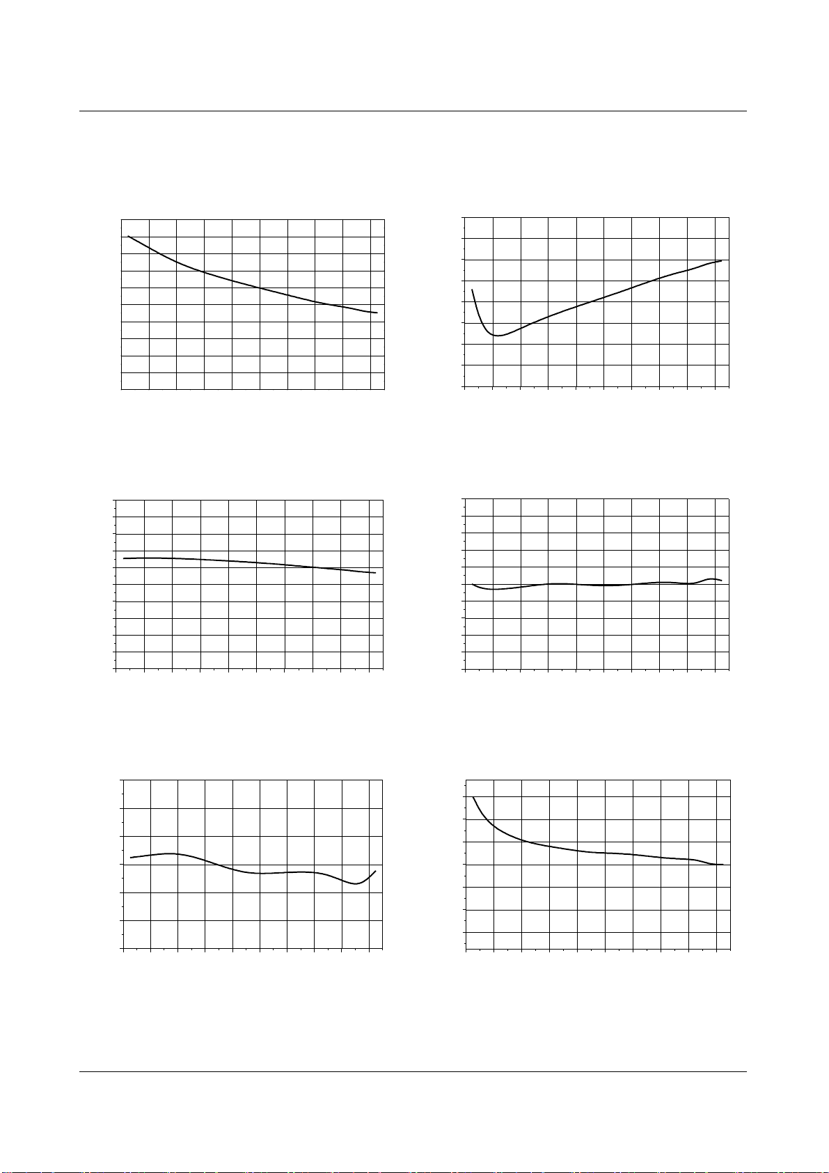
Figure 7. Start-Up Supply Current vs Temperature
Fig9. Sink Current vs Temperature
10
9
8
7
6
5
4
3
EA Sink Current(mA)
2
1
0
-40 -20 0 20 40 60 80 100 120 140
Ambient Temperature(℃)
Fig8. E.A. Source Current vs Temperature
-2
-3
-4
-5
-6
-7
EA Source Current(mA)
-8
-9
-10
-40 -20 0 20 40 60 80 100 120 140
Ambient Temperature(℃)
Figure 8. EA Source Current vs Temperature
Fig.10 Input Bias Current vs Temperature
0.5
0.4
0.3
)
0.2
㎂
0.1
0.0
-0.1
-0.2
EA Input Bias Current(
-0.3
-0.4
-0.5
-40 -20 0 20 40 60 80 100 120 140
Ambient Temperature(℃)
Figure 9. EA Sink Current vs Temperature
Fig.11 Multiplier Gain vs Temperature
0.75
0.70
0.65
0.60
0.55
Multiplier Gain(1/V)
0.50
0.45
-40 -20 0 20 40 60 80 100 120 140
Ambient Temperature(℃)
Figure 11. Multiplier Gain vs Temperature
8
Figure 10. EA Input Bias Current vs Temperatur
Fig.12 Idet Threshold High vs Temperature
1.92
1.88
1.84
1.80
1.76
Idet Threshold High(V)
1.72
1.68
-40 -20 0 20 40 60 80 100 120 140
Ambient Temperature(℃)
Figure 12. Idet Threshold Volyage vs Temperature
Page 9
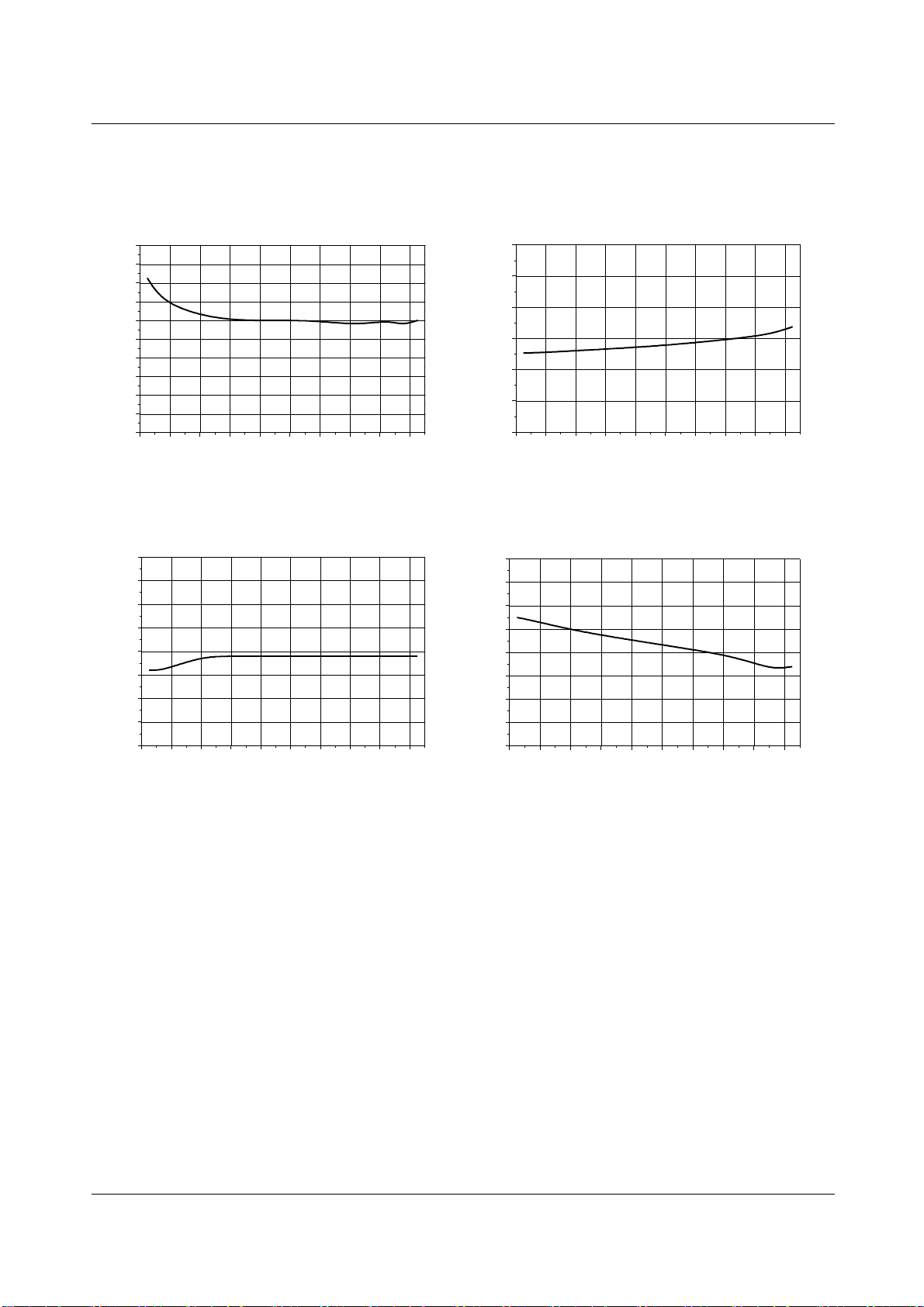
Typical Performance Characteristics (continued)
KA7526
Fig.13 Idet Input Hysteresis vs Temperature
400
360
320
280
240
200
160
120
Idet Input Hyster esis(mV)
80
40
0
-40-200 20406080100120140
Ambient Temperature(℃)
Figure 13. Idet Input Hysteresis vs Temperature
Fig.15 Max. Mult . O utp ut Vo lta ge vs Tem per at ur e
1.85
1.80
1.75
1.70
1.65
1.60
1.55
Max. Multi Output Voltage(V)
1.50
1.45
-40 -20 0 20 40 60 80 100 120 140
Ambient Temperature(℃)
Fig.14 Restart Time vs Temperature
600
500
400
)
㎲
300
Restart Time(
200
100
0
-40-200 20406080100120140
Ambient Temperature(℃)
Figure 14. Restart Time vs Temperature
Fig.16 Supply Current vs Temperature
8
7
6
5
4
3
Supply Current(mA)
2
1
0
-40 -20 0 20 40 60 80 100 120 140
Ambient Temperature(℃)
Figure 15. Max.Mult.Output Voltage vs Temperature
Figure 16. Supply Current vs Temperature
9
Page 10
KA7526
Operating Description
KA7526 is high performance, critical conduction, current-mode power facto r contro ller specifically designed for use in offline active preconverters with minimal external components. This device provides the necessary features which are required to
significantly en-hance poor power factor loads by keeping the ac line current sinusoidal and in phase with the line voltage.
KA7526 contains many of the building blocks and protection features that are employed in modern high performance current
mode power supply controllers. A description of each of the function blocks is given below.
START-UP
An Undervoltage Lockout comparator has been incorporated to guarantee that IC is fully functional before enabling the output
stage. The positive power supply terminal (Vcc) is monitored by the UVLO comparator with the upper threshold set at 13V
and the lower threshold at 8V. In the stand-by mode, with Vcc at 12.5V, the required supply current is less than 0.3mA . This
large hysteresis and low start-up current allow the implementation of efficient bootstrap start-up techniques, making this
device ideally suited for wide range off-line preconverter applications.
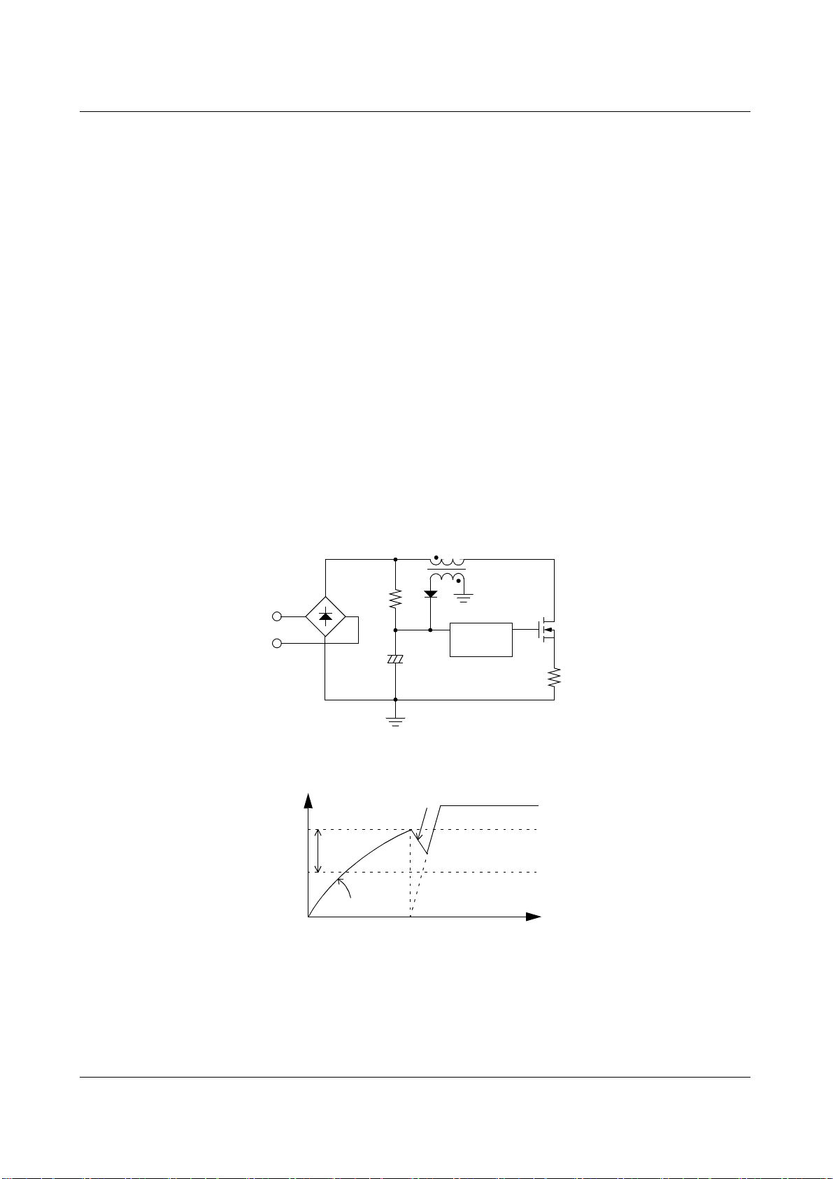
Fig.1.1 shows the start-up circuit. Circuit operation is as follows:
The start-up capacitor (Cst) is charged by current through start-up resistor (Rst) minus the start-up current drawn by the IC.
Once the capacitor voltage reaches the start-up threshold, the IC turns on, starting the switching of the MOSFET. The operation of the IC demands an increase in operating current which results in discharging the capacitor. Before the start-up capacitor
voltage is dischar g ed below hyste res is vol tage, the auxi liar y wind ing voltag e takes over as the su pply vo lta ge as sho wn in F ig.
1.2.
AC
input
Vstart
Vcc
Rst
Cst
+
DVcc
Vcc
Fig.1.1 Start-up Circuit
Cst discharges
Hysteresis
Cst charges
from Rst
Fig.1.2 Star t-up Capacitor Voltage
Out
KA7526
t
10
Page 11
KA7526
Error Amplifier
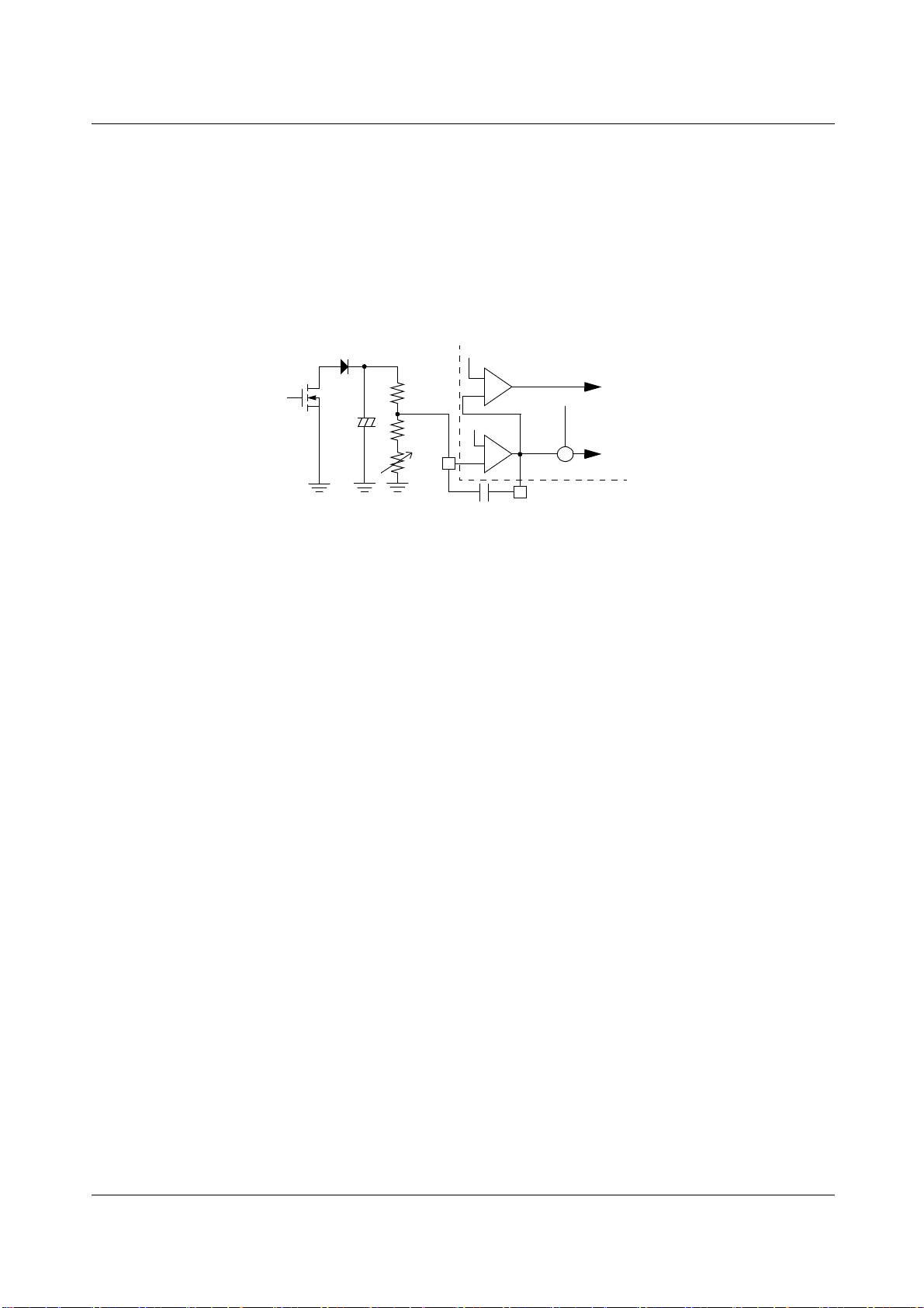
An Error Amplifier with access to the inverting input and output is provided. The noninverting input is internally biased at
2.5V and is not pinned out. The output voltage of the power factor converter is typically divided down and monitored by the
inverting input. The error amp output is internally connected to the multiplier and is pinned out for external loop compensation. Typically, the loopbandwidth is set below 20Hz, so that the amplifer’s output voltage is relatively constant over a given ac
line cycle. In effect, the error amp monitors the average output voltage of the converter over several line cycles. Input bias current(0.5uA, max) can cause an output voltage error that is equal to the product of the input bias current and the value of the
upper divider resistor, R1 in Fig. 2.1.
1.8V
Over Voltage
Comparator
+
R1
+
R2
R3
INV
Band width= 1/(2π×R1×Ccomp)
Fig.2.1 Error Amp and Over Voltage Comparator
-
Vref
+
-
1
Ccomp
2
EA OUT
Vref
+
To Drive
Output Shutdown
_
x
To Multiplier
Over Voltage Protection
The low bandwidth (typically below 20Hz) characteristic of Error Amplifier control loop results in output voltage runaway
condition. This condition can occur during initial start-up, sudden load removal, or during output arcing. The over voltage
comparator monitors the output voltage of the error amplifier. When load is removed, error amp output swings lower than
1.8V, comparator is triggered high and output driver is turned off till the error amp inverting input voltage drops below 2.5V.
At this point, the error amp output swings positive, turns the output driver back on. .
Multiplier
A single quadrant, two input multiplier is the critical element that enables this device to get power factor correction. One input
of multiplier(Pin 3) is connected to an external resistor divider which monitors the rectified ac line. The other input is internally driven by a DC voltage which is the difference of error amplifier output (Pin 2) and reference voltage, Vref. The multiplier is designed t o have an ext reme ly lin ear t ransf er cur ve ov er a w ide dy namic range , 0V to 3.8V for Pi n 3, a nd 2.5V to 4. 5V
for error amplifier output under all line and load conditions.
The multiplier output controls the current sense comparator threshold as the ac voltage traverses sinusoidally from zero to
peak line. This allows the inductor peak current to follow the ac line thus forcing the average input current to be sinusoidal. In
other words, this has the effect of forcing the MOSFET on-time to track the input line voltage, resulting in a fixed drive output
on-time, thus making the preconverter load appear to be resistive to the ac line.
The equation below describes the relationship between multiplier output and inputs.
Vmo = K × Vm1 × (Vm2-Vref)
K : Multiplier gain
Vm1: Voltage at Pin 3
Vm2: Error amp output voltage
Vmo: Multiplier output voltage
11
Page 12
KA7526
Current Sense
Comparator
-
+
CS
+
4
3
MULT
1.65V
Vm1
Vmo
Vref
+
Error Amp
Vm2
+
2
EA OUT
.
+
-
1
INV
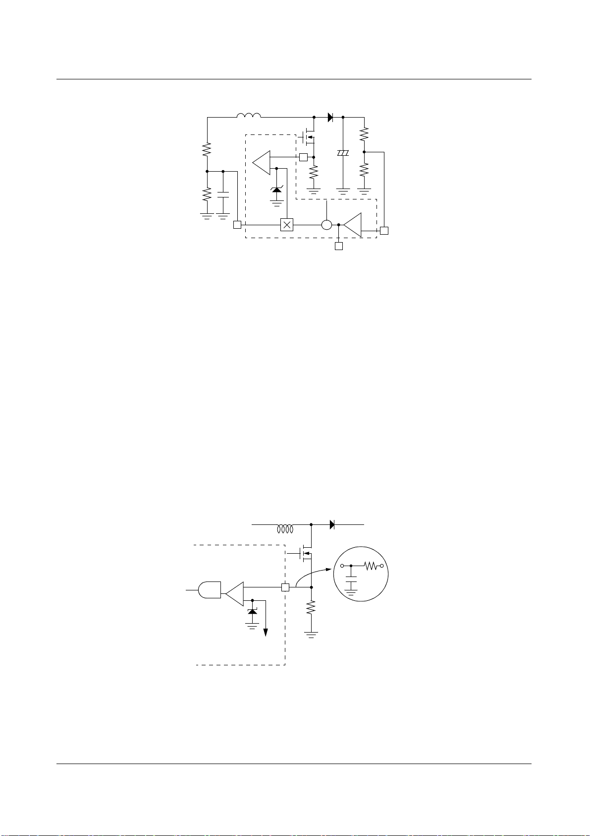
Fig.3.1 Multiplier Block
Current Sense Comparator
The current sense comparator adopt the RS latch configuration to ensure that only a single pulse appears at the drive output
during a given cycle. MOSFET drain current is converted to voltage using an external sense resistor in series with the external
power MOSFET. When sense voltage exceeds the threshold set by the multiplier output, the current sense comparator terminates the gate drive to the MOSFET and resets the PWM latch. The latch insures that the output remains in a low state after the
MOSFET drain current falls back to zero.
The peak inductor current under normal operating conditions is controlled by the mu ltiplier output , Vmo.
Abnormal operating conditions occur during preconverter start-up at extremely high line or as output voltage sensing is lost.
Under these conditions, the multiplier output and current sense threshold will be internally clamped to 1.65V. Therefore, the
maximum peak switch current is limited to:
Ipk(max) = 1.65V / Rsense
An internal R/C filter has been included to attenuate any high frequency noise that may be present on the current waveform.
This circuit block eliminates the need for an external R/C filter otherwise required for proper operation of the circuit.
12
cs
Multiplier
Output
4
Rsense
+
-
1.65V
Fig. 4.1 Current Sense Circuit
External R/C Filter
can be eliminated
Page 13

KA7526
Zero Current Detector
KA7526 operates as a critical conduction current mode controller. The power MOSFET is turned on by the zero current detector and turned off when the peak inductor current reaches the threshold level established by the multiplier output. The slope of
the inductor current is indirectly detected by monitoring the voltage across a separate winding and connecting it to the zero
current detector Pin 5.
Once the inductor current reaches ground level, the voltage across the winding reverses polarity. When the Idet input falls
below 1.8V, the comparator output is triggered to the low state.
To prevent false tripping, 240mV of hysteresis is provided. The zero current detector input is internally protected by two
clamps.
The upper 7.5V clamp prevents input over voltage breakdown while the lower 0.75V clamp prevents substrate injec tion. An
internal current limit resistor protects the lower clamp transistor in case the Idet pin is accidently shorted to ground.
A watchdog timer function was added to the IC to eliminate the need for an external oscillator when used in stand-alone applications. The timer provides a means to automatically start or restart the preconverter if the drive output has been off for more
than 300us after the inductor current reaches zero.
Drive Output
The KA7526 contains a single totem-pole output stage specifically designed for direct drive of power MOSFET. The drive
output is capable of up to 500mA peak current with a typical rise and fall time of 130ns, 50ns each with a 1.0nF load. Additional internal circuitry has been added to keep the drive output in a sinking mode whenever the UVLO is active. This characteristic eliminates the need for an external gate pull-down resistor. Internal voltage clamping ensures that output driver is
always lower than 13V when supply voltage variation exceeds more than rated Vgs threshold (typ 20V) of the external MOSFET. This eliminates an external zener diode and extra power dissipation associated with it that otherwise is required for reliable circuit operation.
13
Page 14
KA7526
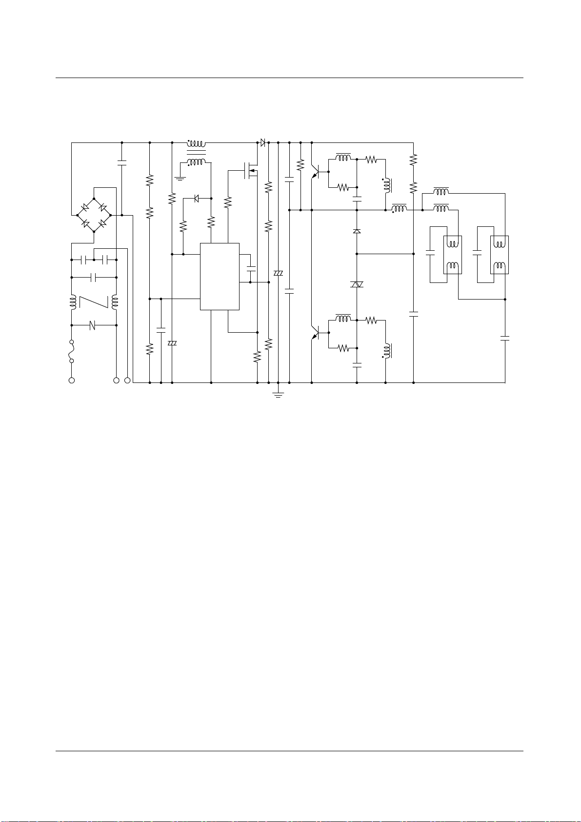
APPLICATION CIRCUIT #1
< 90 ~ 265VAC Input, 400VDC, 32W×2 Lamps Self-oscillating Ballast >
D1
C2
Fuse
AC
Input
L2
C4
R1
D3
D4
D2
C3
C1
L1
V1
GND
R4
R2
C7
R3
D6
R5
R7
5
7
8
KA7526
IC 1
3
4
6
+
C5
D5
L6
R14
Q1
R9
R6
R10
2
C6
1
+
C8
R11
R8
Q2
C9
C10
R13
C11
D7
D8
L7
R16
Q3
R15
C12
L5
L5
L5
R17
L3
R18
L4
Lamp
1
C14 C15
C13
Lamp
2
C16
14
Page 15
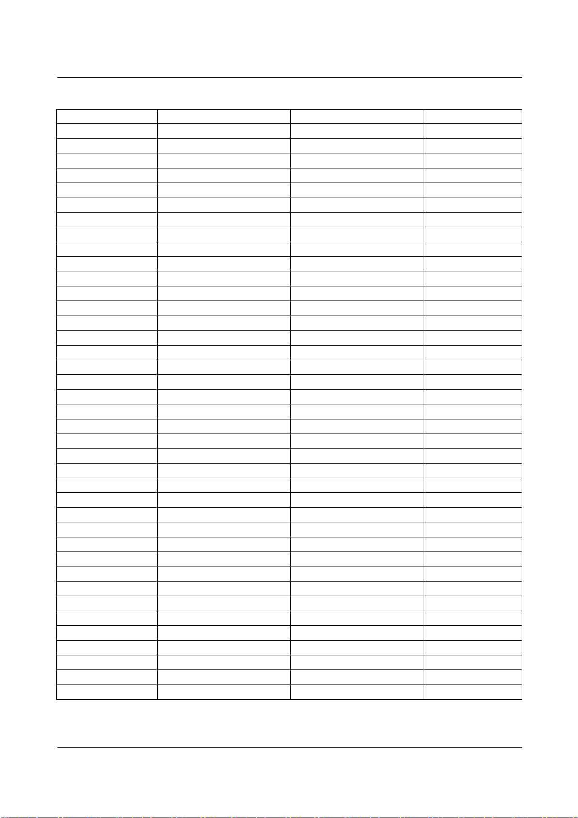
Component Listing (for Application circuit #1)
Reference Value Part Number Manufacturer
R1, 2 1.2MΩ-F, 1/4W 26mm Type -
R3 11kΩ-F, 1/4W 26mm Type R4 150kΩ , 1/2W 26mm Type R5 22kΩ-J, 1/4W 26mm Type -
R6, 13, 15 47Ω-J, 1/4W 26mm Type -
R7 3.3Ω, 1/4W 26mm Type -
R8 1Ω-J, 1W 26mm Type R9 180kΩ-F, 1/4W 26mm Type -
R10 820kΩ-F, 1/4W 26mm Type -
R11 6.8kΩ-F, 1/4W 26mm Type -
R12, 17, 18 390kΩ-J, 1/4W 26mm Type -
R14, 16 8.2Ω-J, 1/4W 26mm Type -
C1 0.15uF, 630V MEP-CAP -
C2, 3 2200pF, 3000V Y-CAP -
C4 0.22uF, 630V MPE-CAP C5 22uF, 35V Electrolytic C6 0.33uF, 25V Ceramic C7 1000pF, 50V Ceramic C8 47uF, 450V Electrolytic C9 4700pF, 630V PPF-CAP -
C10 2200pF, 630V PPF-CAP -
C11, 12 0.15uF, 63V MPF-CAP -
C13 0.1uF, 50V Ceramic -
C14, 15 8200pF, 1000V PP-CAP -
C16 0.15uF, 630V MEP-CAP -
D1, 2, 3, 4, 7 1000V, 1A IN4007GP -
D5 1000V, 1.5A BYV26C Philips
D6 75V, 150mA IN4148 D8 - N413N (DIAC) -
L1 DR 10×12 DIT-010 -
L2 EI 2519 DBT-002 -
L3, 4 EI 2820 DPT-086 -
L5 SB5S 8×3×4 DDT-005 -
L6, 7 10uH BS24-100K Fuse - 52NM250V, 3A -
V1 430V INR140, 431 -
IC1 - KA7526 FairChild
Q1 500V, 4.5A QFP6N50 FairChild
Q2, 3 400V, 5A KSC5305D FairChild
KA7526
15
Page 16
KA7526
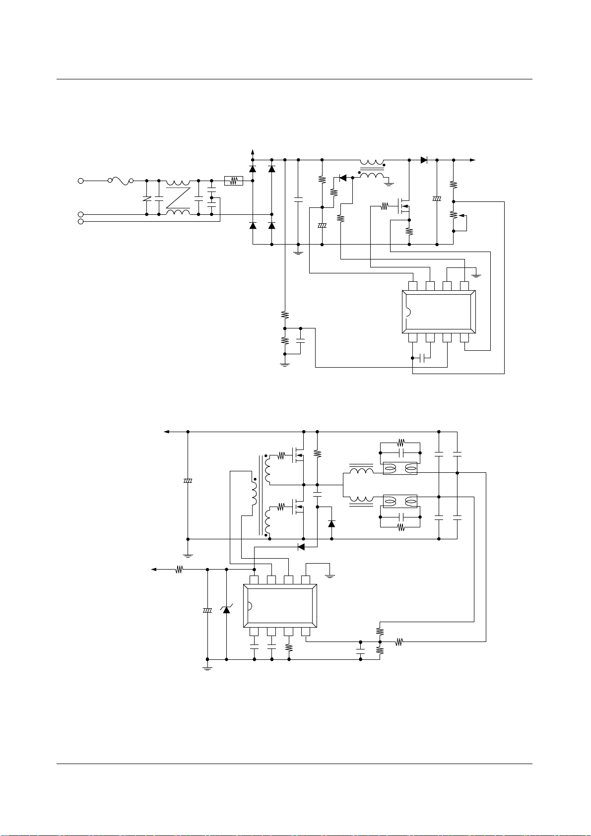
Application Circuit #2
< 90 ~ 265VAC Input, 400VDC, 32W×2 Lamps External-oscillating Ballast >
Full-wave Rectified Output
Fuse
AC Input
V1
C1
L1
C2
C4
C3
NTC
D2
D1
D3
C5
D4
D6
R3
R6
+
C6
R4
L2
Q1
R5
8 765
R7
D5
C9
PFC Output
R8
+
R9
To PFC Output
To Full-wave
Rectified
Output
C9
R12
R1
R2
T1
+
8 765
R10
R11
Q2
Q3
C8
D8
R14
C14
D7
L4
C15
L3
Lamp1
Lamp2
R16
KA7526
1234
C7
R15
C17
R16
C18
C20
C19
16
C10
+
Z1
KA7541
1234
C11
C12
R13
C13
R17
R18
R19
Page 17
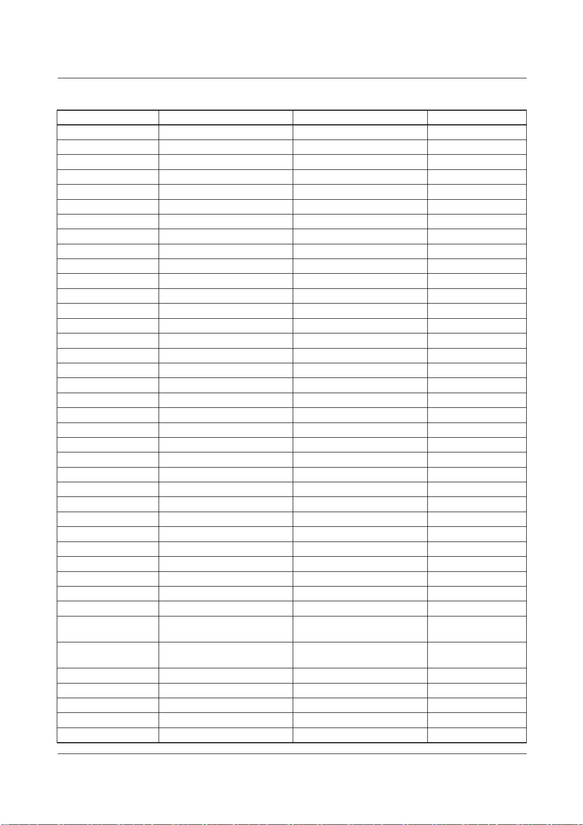
Component Listing (for Application Circuit #2)
Reference Value Part Number Manufacturer
R1 2.2MΩ-F, 1/4W 26mm Type R2 12kΩ-F, 1/4W 26mm Type -
R3, 12 150kΩ , 1/2W 26mm Type -
R4 22kΩ-J, 1/4W 26mm Type -
R5, 10, 11 47Ω-J, 1/4W 26mm Type -
R6 3.3Ω, 1/4W 26mm Type -
R7 1Ω-J, 1W 26mm Type R8 1.2MΩ-F, 1/4W 26mm Type -
R9 10kΩ Variable Resistor - R13 22kΩ-F, 1/4W 26mm Type R14 180kΩ-J, 1/4W 26mm Type -
R15, 16 330kΩ-J, 1/4W 26mm Type R17, 18 680kΩ-J, 1/4W 26mm Type -
R19 8.2kΩ-J, 1/4W 26mm Type -
C1, 2 0.15uF, 630V MEP-CAP C3, 4 2200pF, 3000V Y-CAP -
C5 0.1uF, 400V MPE-CAP -
C6 22uF, 35V Electrolytic -
C7 0.33uF, 25V MPE-CAP -
C8 0.01uF, 25V MPE-CAP -
C9 47uF, 450V Electrolytic C10 47uF, 35V Electrolytic -
C11 0.22uF, 25V MPE-CAP C12 180pF, 25V Ceramic C13 0.1uF, 25V MPE-CAP C14 1000pF, 630V MPE-CAP -
C15, 16 4700pF, 1000V MPE-CAP -
C17, 18, 19, 20 6800pF, 630V MPE-CAP -
D1, 2, 3, 4 1000V, 1A 1N4007 -
D5 FRD(25nS) BYV26C Philips
D6 75V, 150mA 1N4148 -
D7,8 1000V, 1.5A 1N4937 -
L1 80mH BSF2125 L2
L3, 4
T1 1.2mH(35T:24T:24T) EE1614 -
Fuse - 52NM250V, 3A -
V1 430V INR140, 431 -
Q1, 2, 3 500V, 6A SKP6N50 FairChild
Z1 15V, 1W - -
1.2mH (100T: 7T)
Litz Wire or USTC
3.1mH
Litz Wire or USTC
EI2820 -
EI2820 -
KA7526
17
Page 18
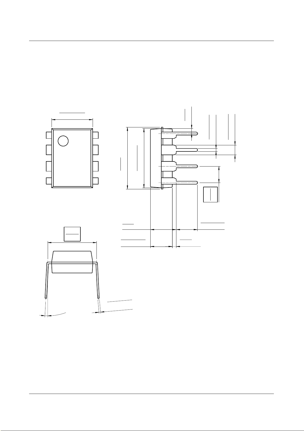
KA7526
Mechanical Dimensions
Package
6.40
±0.20
0.252
±0.008
8-DIP
Dimensions in millimeters
0.79
0.031
()
±0.10
±0.004
±0.10
±0.004
#1
#8
#4 #5
7.62
0.300
MAX
9.60
0.378
5.08
0.200
3.40
0.134
±0.20
9.20
MAX
±0.20
±0.008
±0.008
0.362
0.33
0.013
MIN
0.46
3.30
0.130
2.54
±0.30
±0.012
0.018
0.100
1.524
0.060
18
0~15°
0.25
0.010
+0.10
–0.05
+0.004
–0.002
Page 19
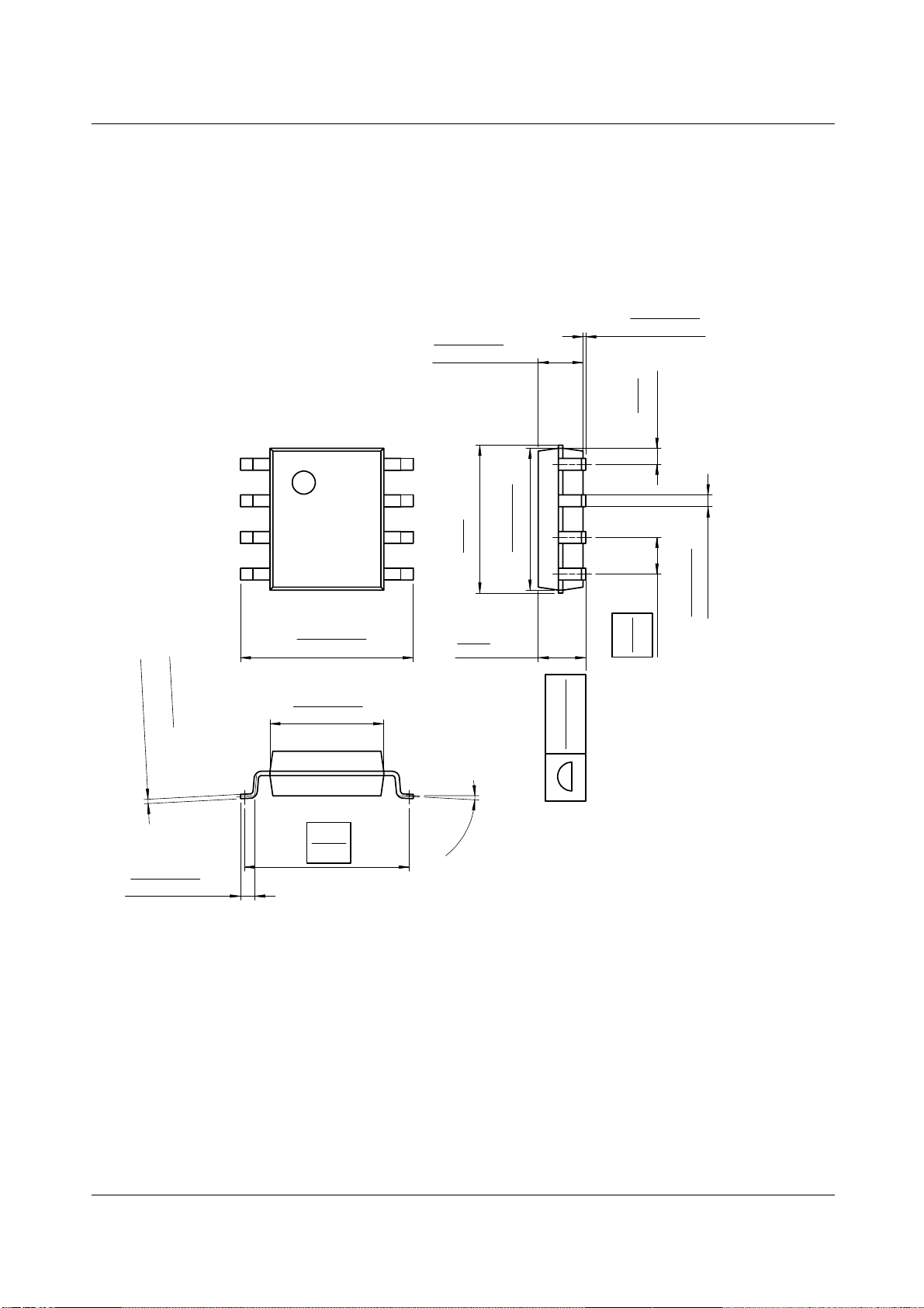
KA7526
Mechanical Dimensions
Package
#1
#4
(Continued)
8-SOP
1.55 ±0.20
0.061 ±0.008
#8
#5
MAX
5.13
0.202
Dimensions in millimeters
0.1~0.25
MIN
0.004~0.001
0.56
0.022
()
4.92 ±0.20
0.194 ±0.008
0.006
0.15
+
-0.002
-0.05
0.004
0.50 ±0.20
0.020 ±0.008
+
0.10
6.00 ±0.30
0.236 ±0.012
3.95 ±0.20
0.156 ±0.008
5.72
0.225
0.071
0~8°
1.80
MAX
MAX0.10
MAX0.004
1.27
0.050
0.41 ±0.10
0.016 ±0.004
19
Page 20

KA7526
Ordering Information
Product Number Package Operating Temperature
KA7526 8-DIP
KA7526D 8-SOP
-25 ~ +125
o
C
20
Page 21

KA7526
21
Page 22

KA7526
DISCLAIMER
FAIRCHILD SEMICONDUCTOR RESERVES THE RIGHT TO MAKE CHANGES WITHOUT FURT HER NOTICE TO ANY
PRODUCTS HEREI N TO IMPROVE RELIABILITY, FUNCTIO N OR DESIGN. FAIRCH IL D DOES NOT ASSUME ANY
LIABILITY ARISING OUT OF THE APPLICATION OR USE OF ANY PRODUCT OR CIRCUIT DESCRIBED HEREIN; NEITHER
DOES IT CONVEY ANY LICENSE UNDER IT S PATENT RIGHTS, NOR THE RIGHTS OF OTHE RS.
LIFE SUPPORT POL I CY
FAIRCHILD’S PR ODUCTS ARE NOT AUTH ORIZED FOR USE AS C RITICAL COMPONENT S IN LIFE SUPPORT DE VICES
OR SYSTEMS WITHOUT THE EXPRESS WRITTEN APPROVAL OF THE PRESIDENT OF FAIRCHILD SEMICONDUCTOR
INTERNATIONAL. As used herein:
1. Life support devices or systems are devices or systems
which, (a) are intended for surgical implant into the body,
or (b) support or sustain life, and (c) whose failure to
perform when properly used in accordance with
2. A critical component in any component of a life support
device or sy stem whose fai lure to perform can be
reasonably expec ted to cause the failur e of the life support
device or system, or to affect its safety or effec t iv ene ss .
instructions for use provided in the labeling, can be
reasonably expected to result in a significant injury of the
user.
www.fairchildsemi.com
9/25/00 0.0m 001
2000 Fairchild Semiconductor International
Stock#DSxxxxxxxx
 Loading...