

Page 1
KA7541
Simple Ballast Controller
www.fairchildsemi.com
Features
• Internal soft start
• Flexible soft start frequency
• No lamp protection
• Trimmed 1.5% internal bandgap reference
• Under voltage lock out with 1.8V of hysteresis
• Totem pole output with high state clamp
• Low start up and operating current
Descriptions
The KA7541 provides simple and high performance
electronic ballast control functions. KA7541 is optimized for
electronic ballast requiring a minimum b oard area, reduced
component count and low power dissipation. Internal soft
start circuitry eliminates the need for an external soft sta rt
PTC resistor. The initial soft start switching frequency and
soft start time can be adjusted depending on the types of
lamps. Protection circuitry has also been adde d to prevent
burning out of switches in no lamp condition. output gate
drive circuit clamps power MOSFET gate voltage
irrespective of supply voltage
8-DIP
1
8-SOP
1
©2001 Fairchild Semiconductor Corporation
Rev. 1.0.3
Page 2
KA7541
Internal Block Diagram
0.22µF
180pF
22k
1.8V
UVLO
+
−
9.5V
8
V
CC
V
CC
OUT 1
7
V
CC
OUT 2
6
GND
5
2V Ref
V
40k
30k
5pF
Z
3pF
2k
−
+
Vref
I
H
I
+
S
R
latch
+
Q
C
Oscilator
I
S
Shut down signal
Ict
+
-
3V
-
+
1V
Ω
−
+
Vref
Ω
Ω
−
+
2V
Ik = IS / 6
Oscilator
Current
mirror
Internal
bias
UVLO
F.D
Frequency
divider
I
= Ik × (Vref − VSS) / Vref
H
= Vref / RS
I
S
Ldet
1
2.5µA
2
8Ict
3
4
C
S
Ct
R
S
Ω
Absolute Maximum Ratings
Parameter Symbol Value Unit
Supply voltage V
Peak drive output current I
Drive output clamping diodes
V
O>VCC
, or VO<−0.3
OH
Iclamp ±10 mA
Soft start, and no lamp detection input voltage V
CC
, I
IN
OL
30 V
±300 mA
−0.3 to 6 V
Operating temperature range Topr -25 to 125 °C
Storage temperature range Tstg −65 to 150 °C
Power dissipation
Thermal resistance (Junction-to-air)
8-DIP
8-SOP 0.5
8-DIP
8-SOP 165
Pd
θja
0.8
100
Absolute Maximum Ratings (-25°°°°C≤≤≤≤Ta≤≤≤≤125°°°°C)
Parameter Symbol Value Unit
Temperature stability for reference voltage (Vref) ∆Vref(Typ) 15 mV
Temperature stability for operating frequency (fos) ∆fos(Typ) 5 kHz
W
°C/W
2
Page 3
Pin Assignments
KA7541
V
1
S
CC
8C
Ct
R
Ldet
2
S
3
4
7
6
5
(Top View)
Pin Definitions
Pin Number Pin Name Pin Function Descrition
1C
2C
3R
S
T
S
4 Ldet
5 GND The ground potential of all the pins.
6OUT 2
7OUT 1
8V
CC
Soft start capacitor connection pin. The pin voltage determines the phase of soft
start, normal mode.
Timing capacitor connection pin. The timing capacitor is charged and discharged
to generate the sawtooth waveform that determines the oscillation frequency in
the internal oscillator block.
Soft start resistor connection pin. The soft start resistor value determines the initial
preheating switching frequency during soft start mode.
Input to the protection circuit. If the pin voltage is lower than 2V, the output of the
gate driver is inhibited.
The output of a high-current power driver capable of driving the gate of a power
MOSFET
The output of a high-current power driver capable of driving the gate of a power
MOSFET.
The logic and control power supply connection.
OUT1
OUT2
GND
3
Page 4
KA7541
Electrical Characteristics
o
Unless otherwise specified, for typical values Vcc=14V, Ta=25
temperature range with
-25
o
≤ Ta ≤ 125
C
o
C
and 11V ≤ V
CC
Parameter Symbol Conditions Min. Typ. Max. Unit
UNDER VOLTAGE LOCK OUT SECTION
Start threshold voltage V
UVLO hysteresis HY
TH(st)
(st)
SUPPLY CURRENT SECTION
Start up supply current I
Operating supply current I
Dynamic operating supply current I
ST
CC
DCC
REFERENCE SECTION
Reference voltage V
Line regulation ∆V
Temperature stability of Vref ∆V
ref
ref 1
ref 2
OSCILLATOR SECTION
Operating frequency fos V
Operating dead time tod V
Soft start frequency fss V
Soft start dead time tsd V
OUTPUT SECTION
Rising time
Falling time
Maximum output voltage V
Output voltage with UVLO activated V
(note1)
(note1)
tr CI=1nF, Vcc=12V - 120 200 ns
tf CI=1nF, Vcc=12V - 50 100 ns
omax(o)VCC
omin(o)
NO LAMP PROTECTION SECTION
No lamp detect voltage Vnd - 1.9 2 2.1 V
Note:
1. These parameters, although guaranteed, are not 100% tested in production.
C, For Min/Max values Ta is the operating ambient
≤ 30V
VCC increasing 8.5 9.5 10.5 V
- 1.3 1.8 2.3 V
VCC<VTH(st) - 0.15 0.25 mA
Output not switching - 6 10 mA
50kHz, CI=1nF - 7 14 mA
Iref=0mA, Vcc=14V 1.95 2 2.05 V
14V≤V
≤25V - 0.1 10 mV
CC
-25≤Ta≤125°C, Vcc=14V - 15 - mV
=3V, CT=470pF 44 50 56 KHz
SS
=3V, Vcc=14V 2.4 2.9 3.4 µs
SS
=0V, CT=470pF 56 65 74 KHz
SS
=0V, Vcc=14V 1.8 2.3 2.8 µs
SS
=20V 12 15 18 V
VCC=5V, IO=100µA--1V
4
Page 5
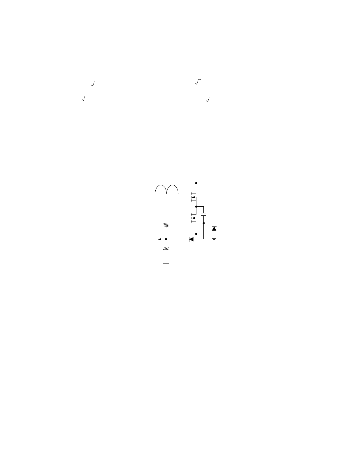
KA7541
Start-up Circuit
Start up current is supplied to the IC through the start up resistor (Rst). In order to reduce the power dissipation in Rst, the Rst
is connected to the full wave rectified output voltage.
The following equation can be used to calculate the size of Rst
Vin ac() 2Vthst()max,–×
-------------------------------------------------------------------------- -
Rst
<
85 2 10.5–×
------------------------------------- - 440kΩ==
0.25 10
×
Ist max,
3–
P
Vin ac_max()2Vcc–⋅()
----------------------------------------------------------------------- -
RSt
2 Vi n ac_max()2Vcc–⋅()
R
×≥
St
R
St
R
260K≥
St
The size of start up capacitor (Cst) is normally decided in terms o f the start up time a nd operating current build up time with
auxiliary operating current source.
The turn off snubber capacitor (Cq2) and two diodes (D1, D2) constitute the auxiliary operating current source for the IC. The
charging current through the Cq2 flows into the IC and also charges the start-up capacitor. If the size of Cq2 is increased, the
V
voltage of the Cst is also increased.
CC
Q1
2
0.5W≤=
2
260K R
440K≤≤∴
St
Rectifier
To V
(Pin 8)
Output
Rst
CC
+
−
Cst
Q2
D2
Cq2
D1
Figure 1. Start up circuit
Oscillator
The gate drive output frequency is as half as that of the triangular waveform in timing capacitor (Ct) at pin #2. In normal
operating mode, the timing capacitor charging current is 50µA. The discharging current is seven times of the charging current
(7× 50µA). The charging period of the timing capacitor is the on duty of the gate drive. The discharging period is the off duty
of the gate drive.
The rising slope and falling slope of the triangular waveform are as following.
Rising slope: dv / dt = i / C = 50µA / Ct
Falling slope: dv / dt = i / C = 7 × 50µA / Ct
For example, when the timing capacitor is 180pF,
∆Tch = 6.69µ
∆Tdis = 0.956µ
5
Page 6

KA7541
Vct
(Pin #2)
Voutput
(Pin #6, 7)
Charging
Period(∆Tch)
Figure 2. Oscillator sawtooth & Output gate drive waveform
Discharging
Period(∆Tdis)
2.86V
1.0V
14V
0V
As a result, the switching frequency is as following
Ts = 2 × (∆Tch + ∆Tdis) = 15.29µ
fsw = 1 / T
= 65KHz
S
The explicit equation calculating the size of the timing capacitor for a certain switching frequency is written below.
C
t
11.76 10
-------------------------------- -=
6–
×
f
sw
Soft Start
The switching frequency is linearly decreasing from the pre-heating frequency to the normal switching fr equency.
In KA7541, the initial pre-heating frequency can be adjusted depending on the types of the lamps used. During the pre-heating
mode, a sixth of the soft start current (I
timing capacitor charging current (50µA). The rising and falling slope o f the triangular waveform are increased due to this
added current .
Soft start current (I
) = 2V / R
S
S
) which flows through the soft start resistor (RS) at pin #3 is added to the normal
S
Rising slope: dv / dt = i / C = (50µA + IS / 6) / Ct
Falling slope: dv / dt = i / C = 7 × (50µA + I
So, once the value of R
and Ct are known, the pre-heating frequency can be calculated straightforward by using the
S
/ 6) / Ct
S
following equation.
6–
0.33
-----------+×
Rs
fsw pre()
50 10
------------------------------------------ -=
Ct 4.25×
The dead time ratio during pre-heating mode is maintained to be constant as well as in normal mode.
(on duty: dead time = 7:1 )
The voltage of the soft start capacitor (C
) determines the soft start time (tss). When VCC voltage exceeds the start-up voltage
S
(Vth(st)), the soft start capacitor start to be charged by the current source (313nA). The switching frequency decreases linearly
to fsw(nor) from fsw(pre) until the soft start capacitor vo ltage (V
) touches 2V. Therefore the soft start duration time (tss)
CS
can be acquired by the following formula.
6
Page 7

Cs V×
----------------- -=
tss
0.2 10
----------------------------------- -
313 10
i
6–
2××
1.28s==
9–
×
For example, the soft start capacitor of 0.2µF makes the soft start time (tss) to be 1.28sec.
fsw, V
CS
fsw (pre)
fsw (nor)
2V
tss
KA7541
Figure 3. Frequency & Soft start capacitor voltage variation during soft start
No Lamp Protection
When the voltage at pin #4 is lower than 2V , the gate drive output is off state, so the external power MOSFET stops switching.
In no lamp protection circuit the dc link voltage is divided by a couple of resistors including both lamp filaments, and The
divided voltage is applied to the pin #4 before the MOSFETs start switching.
R
15KΩ
R
3
4
×++
f
2
4
2
---------------------------------------------------------------------
×=
Vdd
-------------------------------------------------------------------------------------- -------
×
180KΩ
V
3V2
R2R32R
------------------------------------------ R
R
++
1
330KΩ 680KΩ+
-------------------------------------------- - 15KΩ++
--------------------
× 200V≅=
R2R3+
400≅
V
R4
When in normal mode the average voltage of the V3 is the half of the dc link voltage (Vdd). So, in order to make stable start
condition, the resistors are designed to make the voltage of V3 to be the half of the dc link voltage.
7
Page 8

KA7541
DC Link Voltage (Vdd)
V2
Rfilament
Rfilament
To pin #4
R1
Rfilament
R2
Rfilament
V3
R3
R4
C4
Figure 4. Lamp detection resistor networ k
8
Page 9

Application Circuit
<85 ~ 265VAC Input, 400VDC, 32W×2 Lamps Ballast>
KA7541
Full-wave Rectified Output
D3
D1
D4
D2
C5
NTC
C3 C4
C2
L1
C1
TNR
F1
AC INPUT
R1
R2
C8
R3
C6
R6 R4
D6
7
8
Vcc
OUT
FAN7527
INV
EA_OUT
1
2
C7
6
3
L2
GND
MULT
PFC Output
D5
R8
R5
5
Idet
CS
4
Q1
R7
C9
R9
To PFC Output
To full-wave
rectified voltage
R12
C10
Z1
R10
C21
C11
8
Vcc
CS
1
C12
T1
6
7
OUT1
KA7541
Ct
2
3
R11
OUT2
Rs
R13
5
4
GND
Ldet
C13
Q2
Q3
D8
R17
R19
R14
C14
R18
D7
L3
L4
R15
C15
C16
R16
C17
C18
C19
C20
9
Page 10

KA7541
Component Listing
Part number Value Note Manufacturer
R1 2.7MΩ 1/4W -
R2 18kΩ 1/4W R3, 12 150kΩ 1W R4, 13 22kΩ 1/4W -
R5, 10, 11 47Ω 1/4W -
R6 3.3Ω 1/4W -
R7 0.2Ω 1W -
R8 1.2MΩ 1/4W -
R9 103 Variable resistor -
R14 180kΩ 1/4W R15, 16 330kΩ 1/4W R17, 18 680kΩ 1/4W -
R19 15kΩ 1/4W -
C1, 2 150nF, 275vac Box-Cap C3, 4 2200pF, 3000V Y-Cap -
C5 0.22µF, 630V Miller-Cap -
C6, 10 47µF, 35V Electrolytic -
C7 0.33µFMLCC C8 1nF, 25V Ceramic C9 47µF, 450V Electrolytic -
C11, 21 0.22µF, 25V Ceramic -
C12 180pF, 25V Ceramic -
C13 0.1µF, 25V Ceramic -
C14 1nF, 630V Miller-Cap C15, 16 4700pF, 1000V Miller-Cap -
C17, 18, 19, 20 6800pF, 630V Miller-Cap -
Q1, 2, 3 500V, 3.6A FQPF6N50 FairChild
D1, 2, 3, 4 1000V, 1A 1N4007 -
D5 1000V, 1A UF4007 D6 75V, 150mA 1N4148 -
D7, 8 600V, 1A 1N4937 -
ZD1 15V, 1W 1N4744 -
L1 45mH Line Filter L2 590µH (62T:5T) EI3026
L3, 4 3.1mH (120T) EI2820 -
T1 1.2mH(30T:60T) EE1614
F1 250V, 3A Fuse TNR 470V 471 NTC 10Ω 10D09 -
10
Page 11

Mechanical Dimensions
Package
8-SOP
1.55 ±0.20
0.061 ±0.008
Dimensions in millimeters
0.1~0.25
MIN
0.004~0.001
0.56
0.022
()
KA7541
0.006
0.15
+
-0.002
-0.05
0.004
0.50 ±0.20
0.020 ±0.008
+
0.10
#1
#4
6.00 ±0.30
0.236 ±0.012
3.95 ±0.20
0.156 ±0.008
5.72
0.225
#8
#5
0~8°
MAX
5.13
0.202
1.80
0.071
4.92 ±0.20
MAX
0.194 ±0.008
MAX0.10
MAX0.004
1.27
0.050
0.41 ±0.10
0.016 ±0.004
11
Page 12

KA7541
Mechanical Dimensions
Package
6.40
±0.20
±0.008
0.252
#1
#4 #5
#8
(Continued)
9.60
8-DIP
MAX
±0.20
9.20
0.378
±0.008
0.362
Dimensions in millimeters
0.79
0.031
()
±0.10
0.46
2.54
±0.004
0.018
0.100
±0.10
±0.004
1.524
0.060
0~15°
7.62
0.300
0.25
0.010
5.08
0.200
3.40
0.134
+0.10
–0.05
+0.004
–0.002
MAX
±0.20
±0.008
0.33
0.013
MIN
3.30
0.130
±0.30
±0.012
12
Page 13

Ordering Information
Product Number Package Operating Temperature
KA7541 8-DIP
KA7541D 8-SOP
-25°C ~ +125°C
KA7541
13
Page 14

KA7541
DISCLAIMER
FAIRCHILD SEMICONDUCTOR RESERVES THE RIGHT TO MAKE CHANGES WITHOUT FURT HER NOTICE TO ANY
PRODUCTS HEREI N TO IMPROVE RELIABILITY, FUNCTIO N OR DESIGN. FAIRCH IL D DOES NOT ASSUME ANY
LIABILITY ARISING OUT OF THE APPLICATION OR USE OF ANY PRODUCT OR CIRCUIT DESCRIBED HEREIN; NEITHER
DOES IT CONVEY ANY LICENSE UNDER IT S PATENT RIGHTS, NOR THE RIGHTS OF OTHE RS.
LIFE SUPPORT POL I CY
FAIRCHILD’S PR ODUCTS ARE NOT AUTH ORIZED FOR USE AS C RITICAL COMPONENT S IN LIFE SUPPORT DE VICES
OR SYSTEMS WITHOUT THE EXPRESS WRITTEN APPROVAL OF THE PRESIDENT OF FAIRCHILD SEMICONDUCTOR
CORPORATION. As used herein :
1. Life support devices or systems are devices or systems
which, (a) are intended for surgical implant into the body,
or (b) support or sustain life, and (c) whose failure to
perform when properly used in accordance with
2. A critical component in any component of a life support
device or sy stem whose fai lure to perform can be
reasonably expec ted to cause the failur e of the life support
device or system, or to affect its safety or effec t iv ene ss .
instructions for use provided in the labeling, can be
reasonably expected to result in a significant injury of the
user.
www.fairchildsemi.com
9/27/01 0.0m 001
2001 Fairchild Semiconductor Corporation
Stock#DSxxxxxxxx
 Loading...