

Datasheet KA3883D, KA3883, KA3882D, KA3885D, KA3885 Datasheet (Fairchild Semiconductor)
...Page 1
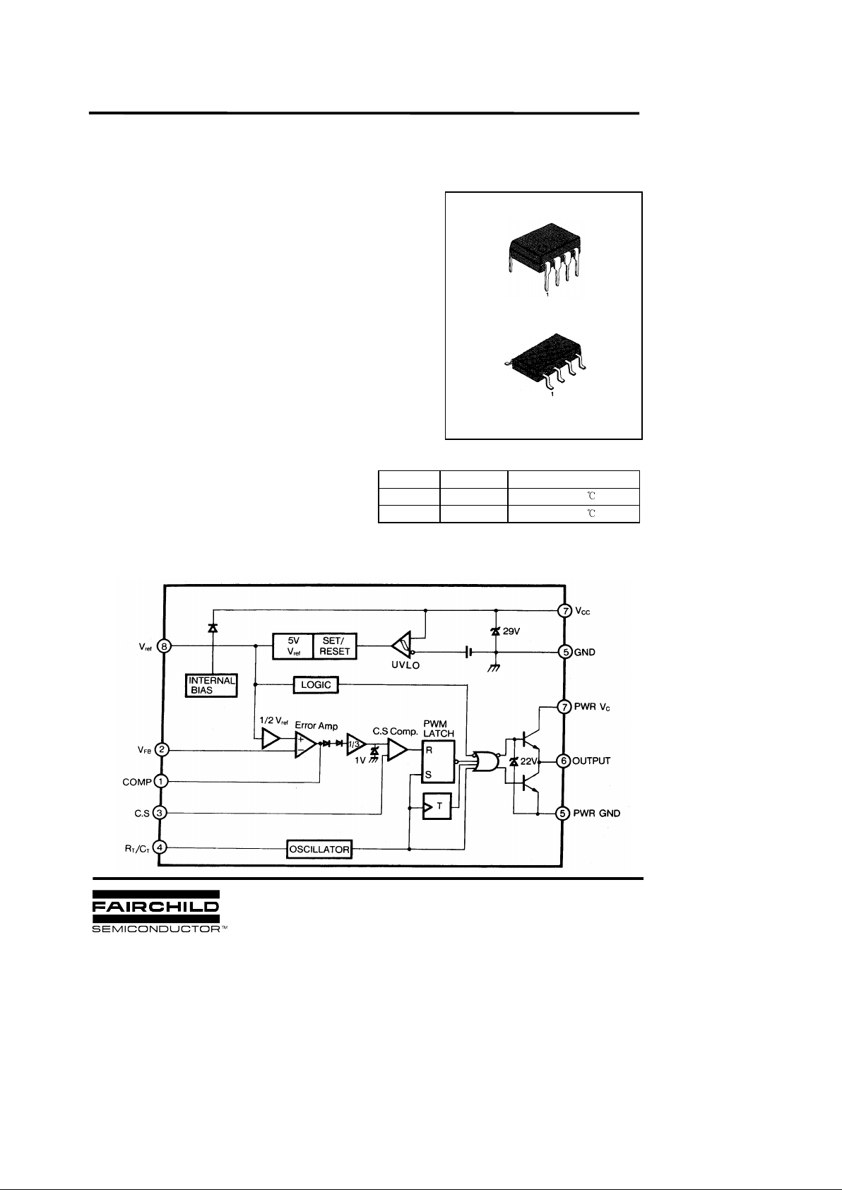
KA3882/3/4/5 SMPS CONTROLLER
CURRENT MODE PWM CONTROLLER
The KA3882/3/4/5 are fixed PWM controller for Off-Line and DC
to DC converter applications. The internal circuits include
UVLO,
low start up current circuit, temperature compensated
reference,
high
gain error amplifier, current sensing comparator, and high
current totempole output for driving a POWER MOSFET. Also KA
3882/3/4/5 provide low start up
current below 0.3mA and short
shutdown delay time typ. 100ns.
The
KA3882 and KA3884 have UVLO threshold of 1 6V(on) and 8 SOP
10V(off).
The KA3883 and KA3885 are 8.4V(on) and 7.6V(off).
The KA3882 and KA3883 can operate within 100% duty cycle.
The KA3884 and KA3885 within 50% by using T Flip-Flop.
FEATURES
• Low Start Current 0.2mA (typ)
• Operating Range Up To 500KHz
• Cycle by Cycle Current Limiting
ORDERING INFORMATI ON
• Under Voltage Lock Out With Hysteresis
• Short Shutdown Delay Time: typ.100ns
• High Current Totempole Output
• Output Swing Limiting: 22V
BLOCK DIAGRAM
Device Package Operating Temperature
KA388X 8 DIP
0 ~ + 85
Î
KA388XD 8 SOP
0 ~ + 85
Î
8 DIP
©1999 Fairchild Semiconductor Co rporation
Rev. B
Page 2
KA3882/3/4/5 SMPS CONTROLLER
ABSOLUTE MAXIMUM RATINGS
ELECTRICAL CHARACTERISTICS
(VCC = 15V, RT = 10K`, CT = 3.3nF, TA = 0Îto + 85Î, Unless otherwise specified)
Characteristic Symbol Value Unit
Supply Voltage V
CC
30 V
Output Current I
O
+ 1 A
Analog Inputs (pin 2, 3) V
I(ANA)
- 0.3 to 6.3 V
Error Amp. Output Sink Current I
SINK(EA)
10 mA
Power Dissipation P
D
1W
Characteristic Symbol Test Conditions Min Typ Max Unit
REFERENCE SECTION
Output Voltage V
REF
TJ = 25Î, IO = 1mA
4.9 5.0 5.1 V
Line Regulation
L
V
REF
VCC = 12V to 25V
ï
620mV
Load Regulation
L
V
REF
IO = 1mA to 20mA
ï
625mV
Output Short Circuit I
SC
Ta = 25
Î
ï
- 100 - 180 mA
OSILLATOR SECTION
Initial Accuracy F
OSC
TJ = 25
Î
47 52 57 KHz
Voltage Stability ST
V
V
CC
= 12V to 25V
ï
0.2 1 %
Amplitude V
OSC
V
PIN4
, Peak to Peak
ï
1.7
ï
V
Discharge Current I
DISCHG
TJ = 25Î, Pin4 = 2V
7.8 8.3 8.8 mA
CURRENT SENSE SECTION
Gain G
V
(NOTE 2, 3) 2.85 3 3.15 V/V
Maximum Input Signal V
I(MAX)
V
PIN1
= 5V(NOTE 2) 0.9 1.0 1.1 V
PSRR PSRR
V
CC
= 12V to 25V
(NOTE 1, 2)
ï
70
ï
dB
Input Bias Current I
BIAS
ïï
- 2 -10 uA
Delay to Output T
D
V
PIN3
= 0V to 2V (NOTE1)
ï
100 200 ns
Page 3

KA3882/3/4/5 SMPS CONTROLLER
ELECTRICAL CHARACTERISTICS(Continued)
(VCC = 15V, RT = 10K`, CT = 3.3nF, TA = 0Îto + 85Î, Unless otherwise specified)
Characteristic Symbol Test Conditions Min Typ Max Unit
ERROR AMPLIFIER SECTION
Input Voltage V
I
T
PIN1
= 2.5V 2.42 2.50 2.58 V
Input Bias Current I
BIAS
ïï
-0.3 - 2 uA
Open Loop Gain G
VO
VO = 2V to 4V
(NOTE 1)
65 90
ï
dB
Unity Gain Bandwidth GBW
T
J
= 25
Î
(NOTE 1)
0.7 1
ï
MHz
PSRR PSRR
V
CC
= 12V to 25V
(NOTE 1)
60 70
ï
dB
Output Sink Current I
SINK
V
PIN2
= 2.7V
V
PIN1
= 1.1V
26
ï
mA
Output Source Current I
SOURCE
V
PIN2
= 2.3V
V
PIN1
= 5.0V
-0.5 -0.8
ï
mA
Output High Voltage V
OH
V
PIN2
= 2.3V
R1 = 15K` to GND
56
ï
V
Output Low Voltage V
OL
V
PIN2
= 2.7V
R1 = 15K` to Pin8
ï
0.8 1.1 V
OUTPUT SECTION
I
SINK
= 20mA
ï
0.1 0.4 V
I
SINK
= 200mA
ï
1.5 2.2 V
I
SOURCE
= 20mA 13 13.5
ï
V
I
SOURCE
= 200mA 12 13.5
ï
V
Rise Time t
R
TJ = 25Î, C1 = 1nF
(NOTE 1)
ï
40 100 ns
Fall Time t
F
TJ = 25Î, C1 = 1nF
(NOTE 1)
ï
40 100 ns
Output Voltage Swing Limit V
OLIM
VCC = 27V, C1 = 1nF
ï
22
ï
V
UNDER VOLTA GE LOCKOUT SECTION
KA3882/4 15 16 17 V
KA3883/5 7.8 8.4 9.0 V
Min.Operating Voltage KA3882/4 9 10 11 V
( After turn on ) KA3883/5 7.0 7.6 8.2 V
Output Low Level V
OL
Output High Level
V
OH
Start Threshold
V
TH
V
TL
Page 4

KA3882/3/4/5 SMPS CONTROLLER
ELECTRICAL CHARACTERISTICS(Continued)
(V
CC
= 15V, RT = 10K`, CT = 3.3nF, TA = 0Îto +85Î, unless otherwise specified)
Adjust V
CC
above the start threshold bifore setting at 15V
NOTE 1. These parameters, although guaranteed, are not 100% tested in production.
2. Parameter measured at trip point of latch with V2 = 0V.
3. Gain defined as: G
V
= LV
PIN1
L
V
PIN3(VPIN3
= 0 to 0.8V)
Characteristic Symbol Test Conditions Min Typ Max Unit
PWM SECTION
KA3882/3 94 96 100 %
KA3884/5 47 48 50 %
Minimum Duty Cycle D
MIN
ïïï
0%
TOTAL STANDBY CURRENT
Start-Up Current I
ST
ïï
0.2 0.4 mA
Operating Supply Current I
CC
V
PIN2
= V
PIN3
= 0V
ï
11 17 mA
VCC Zener Voltage V
Z
ICC = 25mA
ï
29
ï
V
Maximum Duty Cycle
D
MAX
Page 5

TRADEMARKS
ACEx™
CoolFET™
CROSSVOL T™
E2CMOS
TM
FACT™
FACT Quiet Series™
FAST
®
FASTr™
GTO™
HiSeC™
The following are registered and unregistered trademarks Fairchild Semiconductor owns or is authorized to use and is
not intended to be an exhaustive list of all such trademarks.
LIFE SUPPORT POLICY
FAIRCHILD’S PRODUCTS ARE NOT AUTHORIZED FOR USE AS CRITICAL COMPONENTS IN LIFE SUPPORT
DEVICES OR SYSTEMS WITHOUT THE EXPRESS WRITTEN APPROV AL OF FAIRCHILD SEMICONDUCTOR CORPORA TION.
As used herein:
ISOPLANAR™
MICROWIRE™
POP™
PowerTrench™
QS™
Quiet Series™
SuperSOT™-3
SuperSOT™-6
SuperSOT™-8
TinyLogic™
1. Life support devices or systems are devices or
systems which, (a) are intended for surgical implant into
the body, or (b) support or sustain life, or (c) whose
failure to perform when properly used in accordance
with instructions for use provided in the labeling, can be
reasonably expected to result in significant injury to the
user.
2. A critical component is any component of a life
support device or system whose failure to perform can
be reasonably expected to cause the failure of the life
support device or system, or to affect its safety or
effectiveness.
PRODUCT STA TUS DEFINITIONS
Definition of Terms
Datasheet Identification Product Status Definition
Advance Information
Preliminary
No Identification Needed
Obsolete
This datasheet contains the design specifications for
product development. Specifications may change in
any manner without notice.
This datasheet contains preliminary data, and
supplementary data will be published at a later date.
Fairchild Semiconductor reserves the right to make
changes at any time without notice in order to improve
design.
This datasheet contains final specifications. Fairchild
Semiconductor reserves the right to make changes at
any time without notice in order to improve design.
This datasheet contains specifications on a product
that has been discontinued by Fairchild semiconductor.
The datasheet is printed for reference information only.
Formative or
In Design
First Production
Full Production
Not In Production
DISCLAIMER
FAIRCHILD SEMICONDUCTOR RESERVES THE RIGHT TO MAKE CHANGES WITHOUT FURTHER
NOTICE TO ANY PRODUCTS HEREIN TO IMPROVE RELIABILITY, FUNCTION OR DESIGN. FAIRCHILD
DOES NOT ASSUME ANY LIABILITY ARISING OUT OF THE APPLICATION OR USE OF ANY PRODUCT
OR CIRCUIT DESCRIBED HEREIN; NEITHER DOES IT CONVEY ANY LICENSE UNDER ITS PATENT
RIGHTS, NOR THE RIGHTS OF OTHERS.
UHC™
VCX™
 Loading...