

Datasheet KA3845BD, KA3845B, KA3843BD, KA3843B, KA3842BD Datasheet (Fairchild Semiconductor)
...Page 1
www.fairchildsemi.com
KA3842B/KA3843B/KA3844B/KA3845B
SMPS Controller
Features
• Low Start Up Current
• Maximum Duty Clamp
• UVLO With Hysteresis
• Operating Frequency Up To 500KHz
Description
The KA3842B/KA3843B/KA3844B/KA3845B are fixed
frequency current-mode PWM controller. They are specially designed for Off - Line and DC-to-DC converter
applications with minimum external components. These
integrated circuits feature a trimmed oscillator for precise
duty cycle control, a temperature compensated reference,
high gain error amplifier. current sensing comparator, and a
high current totempole output Ideally suited for driving a
power MOSFET. Protection circuity Includes built in
under-voltage lock out a nd cur re nt l imit ing. The KA3842B
and KA3844B have UVLO thresholds of 16V (on) and
10V (off) The KA3843B and KA3845B are 8.5V (on) and
7.9V (off) T he K A3842B and KA3843B c an operate within
100% duty cycle. The KA3844B and KA3845B can operate
with 50% duty cycle.
8-DIP
1
14-SOP
©2000 Fairchild Semiconductor International
1
Rev. 5.0
Page 2
KA3842B/KA3843B/KA3844B/KA3845B
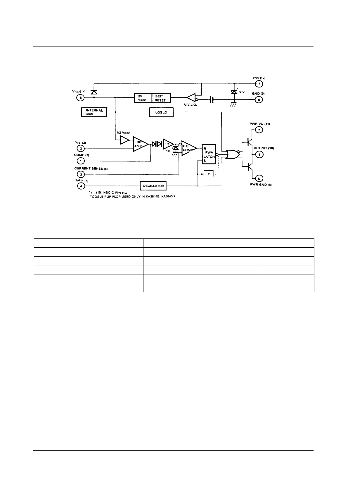
Internal Block Diagram
Absolute Maximum Ratings
Parameter Symbol Value Unit
Supply Voltage V
Output Current I
Analog Inputs (Pin 2.3) V
Error Amp Output Sink Current I
Power Dissipation (T
= 25°C) P
A
CC
O
(ANA)
SINK (E.A)
D
30 V
±1A
-0.3 to 6.3 V
10 mA
1W
2
Page 3
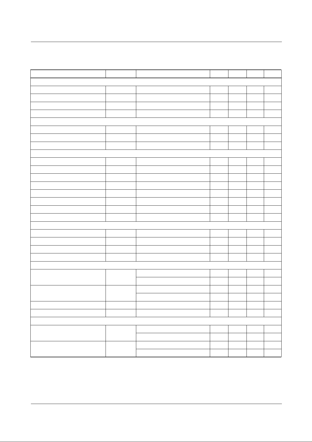
Electrical Characteristics
(VCC=15V, RT=10KΩ, CT=3.3nF, TA= 0°C to +70°C, unless otherwise specified)
Parameter Symbol Conditions Min. Typ. Max. Unit
REFERENCE SECTION
Reference Output Voltage V
Line Regulation ∆V
Load Regulation ∆V
Short Circuit Output Current I
REF
REF
REF
SC
OSCILLATOR SECTION
Oscillation Frequency f T
Frequency Change with Voltage ∆f/∆V
Oscillator Amplitude V
OSC
ERROR AMPLIFIER SECTION
Input Bias Current I
Input Voltage V
Open Loop Voltage Gain G
BIAS
I(E>A)
VO
Power Supply Rejection Ratio PSRR 12V≤ V
Output Sink Current I
Output Source Current I
High Output Voltage V
Low Output Voltage V
SINK
SOURCE
OH
OL
CURRENT SENSE SECTION
Gain G
Maximum Input Signal V
V
I(MAX)
Power Supply Rejection Ratio PSRR 12V≤ V
Input Bias Current I
BIAS
OUTPUT SECTION
V
Low Output Voltage
High Output Voltage
Rise Time t
Fall Time t
OL
V
OH
R
F
UNDER-VOLTAGE LOCKOUT SECTION
Start Threshold
Min. Operating Voltage
(After Turn On)
V
TH(ST)
V
OPR(MIN)
TJ = 25°C, I
12V≤V
1mA≤I
CC
REF
= 1mA 4.90 5.00 5.10 V
REF
≤25V - 6 20 mV
≤20mA - 6 25 mV
TA = 25°C - -100 -180 mA
= 25°C475257KHz
J
CC
12V≤V
≤25V - 0.05 1 %
CC
- -1.6-V
- --0.1-2µA
V1 = 2.5V 2.42 2.50 2.58 V
2V≤ V
≤4V 65 90 - dB
O
≤25V 60 70 - dB
CC
V2 = 2.7V, V1 = 1.1V 2 7 - mA
V2 = 2.3V, V1 = 5V -0.6 -1.0 - mA
V2 = 2.3V, RL = 15KΩ to GND 5 6 - V
V2 = 2.7V, RL = 15KΩ to Pin 8 - 0.8 1.1 V
(Note 1 & 2) 2.85 3 3.15 V/V
V1 = 5V(Note 1) 0.9 1 1.1 V
≤25V (Note 1) - 70 - dB
CC
- --3-10µA
I
= 20mA - 0.08 0.4 V
SINK
= 200mA - 1.4 2.2 V
I
SINK
I
SOURCE
I
SOURCE
= 20mA 13 13.5 - V
= 200mA 12 13.0 - V
TJ = 25°C, CL= 1nF (Note 3) - 45 150 ns
TJ = 25°C, CL= 1nF (Note 3) - 35 150 ns
KA3842B/KA3844B 14.5 16.0 17.5 V
KA3843B/KA3845B 7.8 8.4 9.0 V
KA3842B/KA3844B 8.5 10.0 11.5 V
KA3843B/KA3845B 7.0 7.6 8.2 V
KA3842B/KA3843B/KA3844B/KA3845B
P-P
3
Page 4
KA3842B/KA3843B/KA3844B/KA3845B
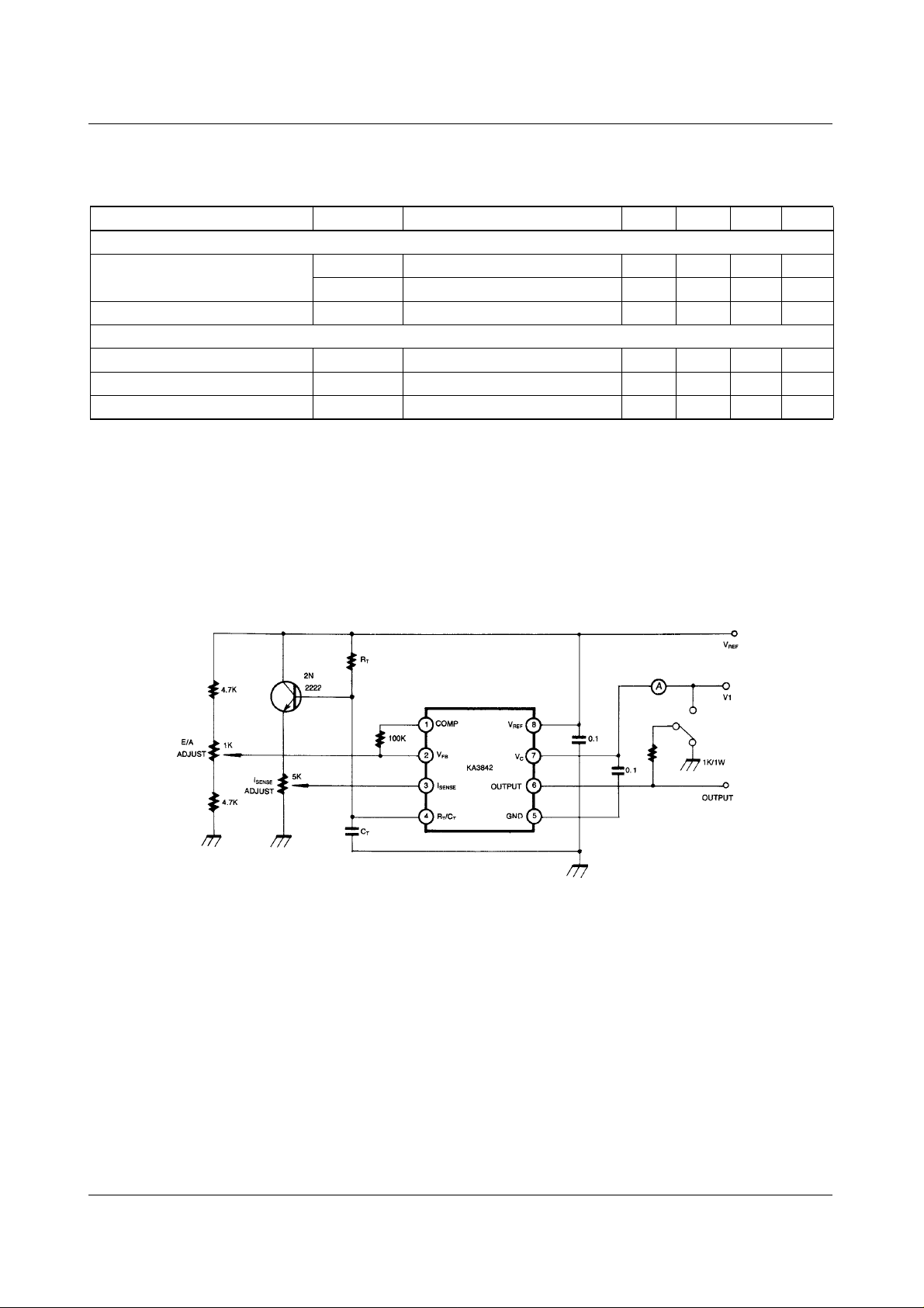
Electrical Characteristics (Continued)
(VCC=15V, RT=10KΩ, CT=3.3nF, TA= 0°C to +70°C unless otherwise specified)
Parameter Symbol Conditions Min. Typ. Max. Unit
PWM SECTION
Max. Duty Cycle
D
Min. Duty Cycle D
TOTAL STANDBY CURRENT
Start-Up Current I
Operating Supply Current I
CC(OPR)
Zener Voltage V
(max)
D KA3844B/KA3845B 47 48 50 %
(MIN)
ST
Z
KA3842B/KA3843B 95 97 100 %
- --0%
- -0.451mA
V3=V2=ON - 14 17 mA
ICC = 25mA 30 38 - V
Adjust V
Note:
1. Parameter measured at trip point of latch
2. Gain def ine d as:
A
3.These parameters, although guaranteed, are not 100 tested in production.
above the start threshould before setting at 15V
CC
∆V
1
----------=
∆V
,0 ≤ V3 ≤ 0.8V
3
Figure 1. Open Loop Test Circuit
High peak currents associated with capacitive loads necessitate careful grounding techniques Timing and bypass capacitors
should be c onnected close to pin 5 in a single point ground. The transistor and 5KΩ potentiometer are used to sample the
oscillator waveform and apply an adjustable ramp to pin 3.
4
Page 5

KA3842B/KA3843B/KA3844B/KA3845B
Figure 2. Under Voltage Lockout
During Under-Voltage Lock-Out, the output driver is biased to a high impedance state. Pin 6 should be shunted to ground
with a bleeder resistor to prevent activating the power switch with output leakage current.
Figure 3. Error Amp Configuration
Figure 4. Current Sense Circuit
Peak current (IS) is determined by the formula:
ISMAX()
1.0V
------------=
R
S
A small RC filter may be required to suppress switch transients.
5
Page 6

KA3842B/KA3843B/KA3844B/KA3845B
Figure 5. Oscillator Waveforms and Maximum Duty Cycle
Oscillator timing capacitor, CT, is charged by V
charge time, the internal clock signal blanks the output to the low state. Selection of R
through RT, and discharged by an internal current source. During the dis-
REF
and C
T
therefore determines both
T
oscillator frequency and maximum duty cycle. Charge and discharge times are determined by the formulas:
= 0.55 RT C
t
c
tDRTCTI
=
Frequency, then, is: f=(tc + td)
ForRT 5KΩ f
T
0.0063RT2.7–
----------------------------------------
n
0.0063R
Figure 6. Oscillator Dead Time & Frequency Figure 7. Timing Resistance vs Frequency
-------------- -=,>
R
1.8
TCT
4–
T
-1
(Deadtime vs CT RT > 5kΩ)
Figure 8. Shutdown Techniques
6
Page 7

KA3842B/KA3843B/KA3844B/KA3845B
Shutdown of the KA3842B can be accomplished by two methods; either raise pin 3 above 1V or pull pin 1 below a voltage
two diode drops above ground. E i the r m ethod causes th e output of the PWM c o mpa r a tor t o be high (refer to block diagra m) .
The PWM latch is reset dominant so that the output will remain low until the next clock cycle after the shutdown condition at
pins 1 and/or 3 is removed. In one example, an externally latched shutdown may be accomplished by adding an SOR which
will be reset by cycling Voc below the lower UVLO threshold. At this point the reference turns off, allowing the SCR to reset.
Figure 9. Slope Compensation
A fraction of the oscillator ramp can be resistively summed with the current sense signal to provide slope compensation for
converters requiring duty cycles over 50%. Note that capacitor, C, forms a filter with R2 to suppress the leading edge switch
spikes.
TEMPERATURE (°C)
Figure 10. TEMPERATURE DRIFT (Vref)
TEMPERATURE (°C)
Figure 12. TEMPERATURE DRIFT (Icc)
TEMPERATURE (°C)
Figure 11. TEMPERATURE DRIFT (Ist)
7
Page 8

KA3842B/KA3843B/KA3844B/KA3845B
Mechanical Dimensions
Package
6.40
±0.20
±0.008
0.252
8-DIP
0.79
0.031
()
±0.10
±0.004
±0.10
±0.004
#1
#8
#4 #5
7.62
0.300
MAX
9.60
0.378
5.08
0.200
3.40
0.134
±0.20
9.20
MAX
±0.20
±0.008
±0.008
0.362
0.33
0.013
MIN
0.46
3.30
0.130
2.54
±0.30
±0.012
0.018
0.100
1.524
0.060
+0.10
0.25
–0.05
+0.004
0.010
–0.002
0~15°
8
Page 9

KA3842B/KA3843B/KA3844B/KA3845B
Mechanical Dimensions
Package
#1
(Continued)
14-SOP
#14
1.55
0.061
MAX
8.70
0.343
±0.10
±0.004
±0.20
8.56
±0.008
0.337
MIN
0.05
0.002
0.47
()
0.10
0.004
-0.05
+
+
0.406
0.019
-0.002
0.016
0.10
+
-0.05
0.20
0.60
0.024
0.004
+
-0.002
0.008
±0.20
±0.008
#7
6.00
0.236
3.95
0.156
5.72
0.225
±0.30
±0.012
±0.20
±0.008
#8
0~8°
1.80
0.071
MAX
MAX0.10
MAX0.004
1.27
0.050
9
Page 10

KA3842B/KA3843B/KA3844B/KA3845B
Ordering Information
Product Number Package Operating Temperature
KA3842B
KA3843B
KA3844B
KA3845B
KA3842BD
KA3843BD
KA3845BD
8 DIP
0 ~ + 70°C
14 SOPKA3844BD
10
Page 11

KA3842B/KA3843B/KA3844B/KA3845B
11
Page 12

KA3842B/KA3843B/KA3844B/KA3845B
LIFE SUPPORT POL I CY
FAIRCHILD’S PR ODUCTS ARE NOT AUTH ORIZED FOR USE AS C RITICAL COMPONENT S IN LIFE SUPPORT DE VICES
OR SYSTEMS WITHOUT THE EXPRESS WRITTEN APPROVAL OF THE PRESIDENT OF FAIRCHILD SEMICONDUCTOR
INTERNATIONAL. As used herein:
1. Life support devices or systems are devices or systems
which, (a) are intended for surgical implant into the body,
or (b) support or sustain life, and (c) whose failure to
perform when properly used in accordance with
2. A critical component in any component of a life support
device or sy stem whose fai lure to perform can be
reasonably expec ted to cause the failur e of the life support
device or system, or to affect its safety or effec t iv ene ss .
instructions for use provided in the labeling, can be
reasonably expected to result in a significant injury of the
user.
www.fairchildsemi.com
7/13/00 0.0m 001
2000 Fairchild Semiconductor International
Stock#DSxxxxxxxx
 Loading...