

Page 1
+
KA2803B
Earth Leakage Detector
www.fairchildsemi.com
Features
• Low Power Consumption PD =5mW, 100V/200V
• Built-in Voltage Regulator
• High Gain Differential Amplifier
• 0.4mA Output Current Pulse to Trigger SCR' S
• Low External Part Count
• DIP Package (8-DIP), High Packing Density
• High Noise Immunity, Large Su rge Margin
• Super Temperature Characteristic of Input Sensitivity
• Wide Operating Temperature Range (T
+80°C)
• Operation from 12 to 20V Input
= -25°C ~
A
Functions
• Differential Amplifier
• Level Comparator
• Latch Circuit
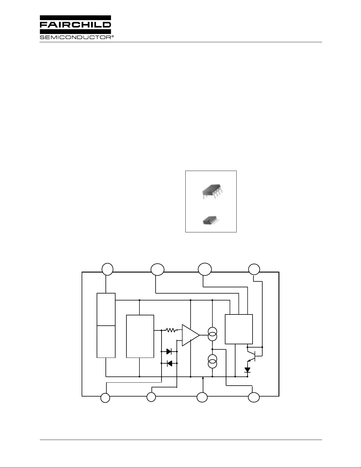
Block Diagram
V
CC
8
7
O
S(Output)
Description
The KA2803B is designed for use in earth leakage circuit
interrupters, for stable operation of the AC line in breakers.
The input of the differential amplifier is connected to the
secondary coil of ZCT(Zero Current Transformer). The
amplified output of differential amplifier is integrated at
external capacitor to gain adequate time delay that is
specified in KSC4613. The level comparator generates high
level when earth leakage current is greater than the fixed
level.
8-DIP
1
8-SOP
1
N
R
6
S
C
5
Bias V ol ta ge
Bias
Internal
Latch
Reference
Voltage
Generator
Reference
Zener Internal
Zener
Protect
1
V
R
©2002 Fairchild Semiconductor Corporation
2
V
I
+
-
3
GND
Latch
Circuit
4
O
D
Rev. 1.0.4
Page 2

KA2803B
Absolute Maximum Ratings (TA = 25°°°°C)
Parameter Symbol Value Unit
Supply Voltage V
Supply Current I
Power Dissipation P
Lead Temperature (Soldering 10sec) T
Operating Temperature T
Storage Temperature T
CC
CC
D
LEAD
OPR
STG
20 V
8mA
300 mW
260 °C
- 25 ~ +80 °C
- 65 ~ +150 °C
Electrical Characteristics
(TA = -25°C to 80°C)
Parameter Symbol Conditions Circuit Min. Typ. Max. Unit
Supply Current 1 I
Trip Voltage V
Differential Amplifier Output
Current 1
Differential Amplifier Output
Current 2
I
O(D)
I
O(D)
Output Current I
Latch on Voltage V
Latch Input Current I
Output Low Current I
SCON
SCON
OSL
Diff. Input Clamp Voltage V
Maximum Current Voltage V
Supply Current 2 I
Latch Off Supply Voltage V
SOFF
Response Time(Note1) T
CC
T
O
IDC
SM
S2
ON
V
= 12V
CC
V
= Open
R
V
= 2V
I
VCC = 16V
V
= 2V ~ 2.02V VI = 2V
R
(-25°C)
1
(80°C) - - 480
2141618mV
(Note1) 12.5 14.2 17 mVrms
VCC = 16V
(V
=30mV , VOD =1.2V)
R-VI
VCC =16V, VOD =0.8V
V
, VI =V
R
P (Note2)
3 -12 20 -30 µA
4172737
VSC = 1.4V (-25°C)
= 0.8V (25°C) 200 400 800
OS
= 16V (25°C) 100 300 600
V
CC
5
VCC = 16V 6 0.7 1.0 1.4 V
V
= 16V 7 -13 -7 -1 µA
CC
VCC = 12V, V
V
= 16V, I
CC
I
= 7mA 10 20 24 28 V
SM
VCC = 12V, V
= 0.2V 8 200 800 1400 µA
OSL
= 100mA 9 0.4 1.2 2 V
IDC
= 0.6V 11 200 400 900 µA
OSL
VOS = 12V
= 1.8V
SC
I
=100mA
IDC
VCC = 16V
V
= 0.3V , 1V < VX < 5V
R-VI
12 7.0 8.0 9.0 VV
13 2 3 4 mS
- - 580
(rms)
200 400 800
µA(25°C) 300 400 530
µA
µAV
Note:
1. This Parameter, although guaranteed, is not tested in Production.
2. V
P=Vpin1
-0.03V at V
pin2
=2.0V , V
pin4
=1.5V
2
Page 3
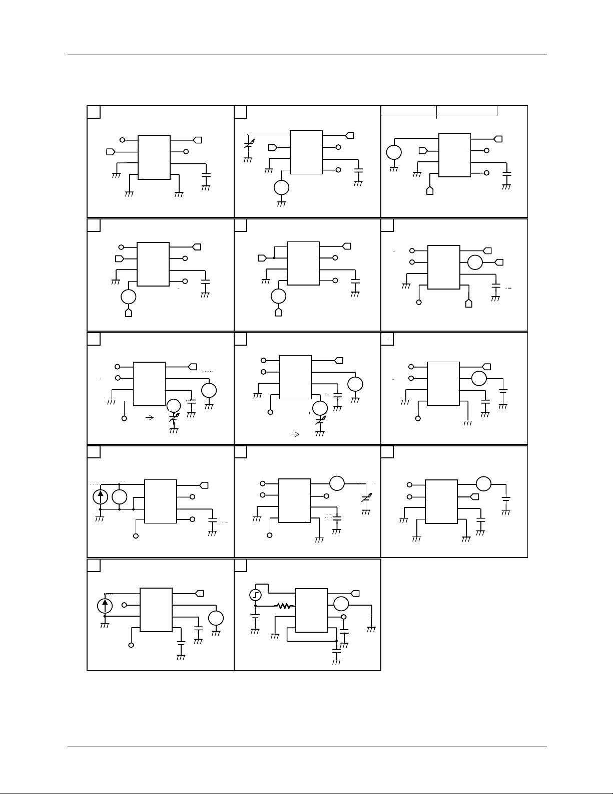
Test Circuit
Supply Current1 Trip Voltage
1
Open
2V
Differential Amplifier Output
3
Current1
Open
V
p
A
1.5V
1
2
3
4
1
2
3
4
I
O(D)=?
KA2803B
V
for VP Measurement
PIN1
473
Pin1 Voltage
Pin1 Voltage
Vpin1
2V
DVM
Output Current
5
1.5V
1
8
7
2
6
3
4
5
* V
p
16V
Open
Open
=Vpin1-0.03V
473
2
8
7
12V
Open
Vr=2V~2.02V
2V Open
6
5
473
Differential Ampl ifie r Outp ut
4
DVM
1
8
7
2
6
3
4
5
16V
Open
Current2
Open
Open
16V
Open
Open
Open
1
8
7
2
6
3
4
5
1.4V
16V
Iout
0.8V
A
473
Open
16V
V
p
8
7
6
5
Open
1
8
2
7
6
3
5
4
I
O(D)=?
A
0.8V
6
Latch on Voltage
Open
Open
9
Diff. Input Clamp Voltage
100mA V
Open
DVM
IDC
1
2
3
4
0.6V
8
7
6
5
1.5V
1
2
3
4
Open
Latch Off Supply Voltage
12
100mA
Open
1
2
3
4
Open
?
8
7
6
5
0.8V
Latch Input Current Output Low Current
7
> 6V
Open
Open
473
16V
DVM
V
1
8
7
2
6
3
4
5
?
16V
DVM
473
A
Open
1.5V
0.6V
Maximum Curr ent Voltage Su p p l y Current2
10
I=7mA
473
Open
Open
Open
Response Time
13
0.3V
p-p
1V<Vx<5
100
8
7
6
5
473
473
A
Open
DVM
>
10V
473
1
8
2
7
3
6
5
4
1
2
3
4
8
7
16V
Open
6
5
Open
12V
DVM
473
> 6V
VSM=?
16V
8
11
Open
Open
Open
Open
Open
A
473
I
cc
A
0.6V
?
=?
473
12V
0.2V
12V
1
8
7
2
6
3
5
4
1
8
7
2
6
3
5
4
3
Page 4
KA2803B
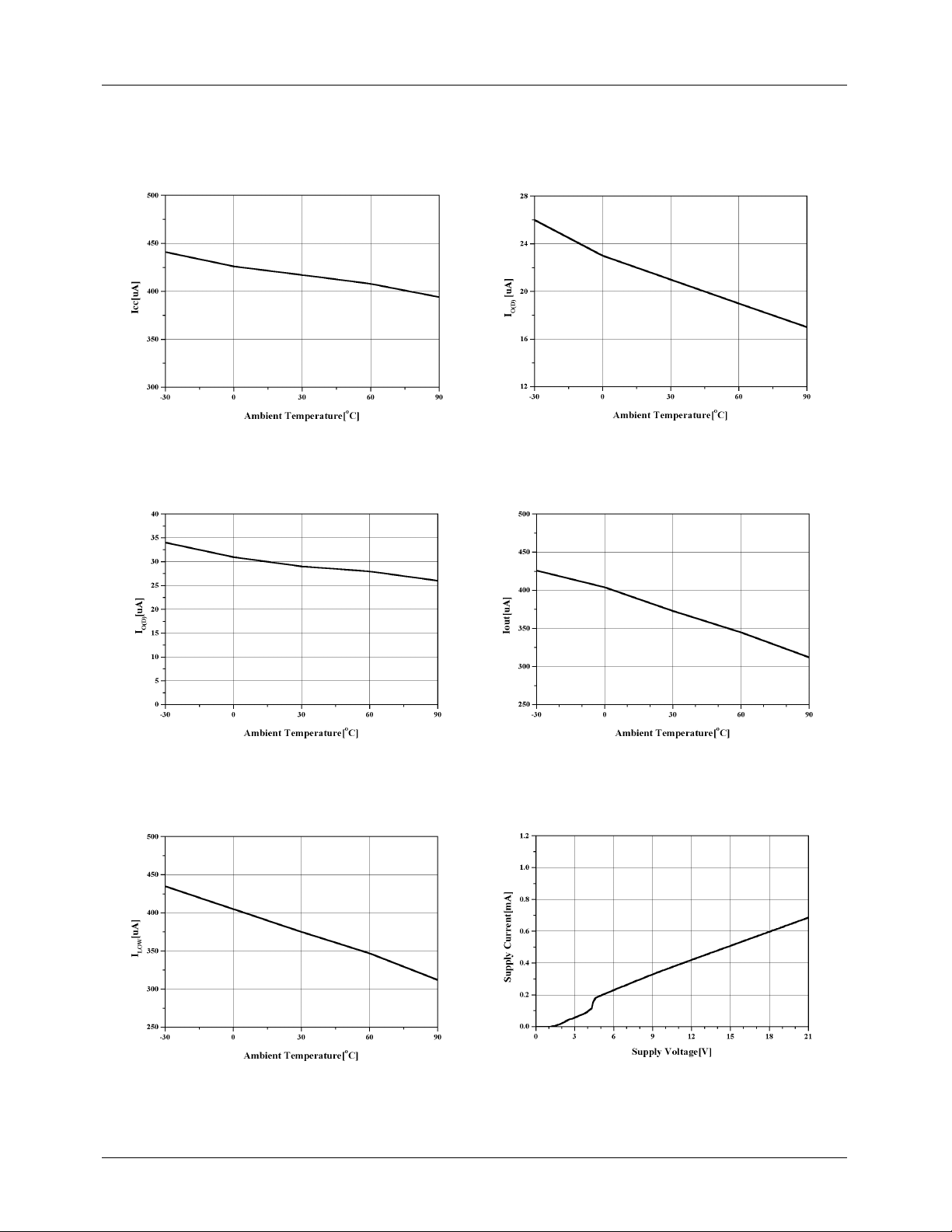
Typical Characteristics
Figure 1. Supply Curre nt
Figure 3. Diffe rential Amp. Output Current
VR, VI=VP, VOD=0.8V
Figure 2. Differential Am p. Output Curre nt
VR-VI=30mV, VOD=1.2V
Figure 4. Output Current
Figure 5. Output Low Current
Figure 6. Vcc Voltage Vs. Supply Current 1
4
Page 5

KA2803B
Typical Characteristics
Figure 7. Differential Amp. Output Current 1
(Continued)
Figure 8. Differential Amp. Output
Figure 9. Latch Input Current
Figure 11. Output Current
Figure 10. Output Low Current
Figure 12. Vcc Voltage Vs. Supply Current 2
5
Page 6

KA2803B
Typical Characteristics
Figure 13. Differenti al Inp ut Clamp Voltage
(Continued)
Figure 14. Latch Off Supply Voltage
Figure 15. Latch On Input Voltage
Figure 17. Trip & Output
Figure 16. Maximum Supply
6
Page 7

KA2803B
Typical Characteristics
INPUT
VR: Variable
: Constant
V
I
OD OUTPUT
OUTPUT
O
S
(Continued)
Figure 18. Output Response Time
7
Page 8

KA2803B
Application Circuit
Figure 1. Full Wave Application Circuit
Figure 2. Half Wave Application Circuit
Application Note
(refer to full wave application circuit Fig. 1)
The Fig 1 shows the KA2803B connected in a typical leakage current detector system.
The power is applied to the V
The resistor R
The value of C
and capacitor CS are chosen so that pin 8 voltage is at least 12V.
S
is recommended above 1µF at this time.
S
If the leakage current is at the load, it is detected by the zero current transformer (ZCT).
The output voltage signal of ZCT is amplified by the differential amplifier of the KA2803B internal circuit and appears as half
cycle sine wave signal referred to input signal at the output of the amplifier.
The amplifier closed loop gain is fixed about 1000 times with internal feedback resistor to compensate for zero current
transformer (ZCT) Variations.
The resistor R
should be selected so that the breaker satisfies the required sensing current.
L
The protection resistor R
to protect the earth leakage detector IC the KA2803B.
The range of R
The capacitor C
is from several hundredΩ to several kΩ.
P
, is for the noise canceller and standard value of C1 is 0.047µF. Also the capacitor C2 is noise canceller
1
capacitance but it is not usually used.
When high noise is only appeared at this system 0.047µF capacitor may be connected between pin 6 and pin 7.
The amplified signal is finally appeared to the Pin 7 with pulse signal through the internal latch circuit of the KA2803B.
This signal drives the gate of the external SCR which energizes the trip coil which opens the circuit breaker.
The trip time of breaker is decided by the capacitor C
This capacitor should be selected under 1µF for the required the trip time.
The full wave bridge supplies power to the KA2803B during both the positive and negative half cycles of the line voltage.
This allows the hot and neutral lines to be interchanged.
If your application want the detail information, request it on our application circuit designer of KA2803B.
terminal (Pin 8) of the KA2803B directly from the power line.
CC
is not usually used put when the high current is injected at the breaker, this resistor should be used
P
and the mechanism breaker.
3
8
Page 9

Mechanical Dimensions
Package
6.40 ±0.20
0.252
±0.008
8-DIP
Dimensions in millimeters
0.79
0.031
()
±0.10
KA2803B
#1
#4 #5
7.62
0.300
#8
MAX
9.20 ±0.20
9.60
0.378
5.08
MAX
0.200
3.40 ±0.20
0.134 ±0.008
0.362 ±0.008
0.33
0.013
3.30 ±0.30
0.130 ±0.012
MIN
0.46
2.54
0.018 ±0.004
0.100
1.524 ±0.10
0.060 ±0.004
0~15°
0.25
0.010
+0.10
–0.05
+0.004
–0.002
9
Page 10

KA2803B
Mechanical Dimensions
Package
#1
#4
6.00
0.006
+
-0.002
0.004
0.15
-0.05
+
0.10
0.236
3.95
0.156
(Continued)
8-SOP
±0.30
±0.012
±0.20
±0.008
#8
#5
1.55
0.061
±0.20
±0.008
MAX
5.13
0.202
1.80
0.071
±0.20
4.92
MAX
Dimensions in millimeters
0.1~0.25
MIN
0.004~0.001
0.56
0.022
()
±0.008
0.194
±0.004
±0.10
0.41
0.016
1.27
0.050
MAX0.10
MAX0.004
10
0.50
0.020
±0.20
±0.008
5.72
0.225
0~8°
Page 11

Ordering Information
Product Number Package Operating Temperature
KA2803B 8-DIP
KA2803BD 8-SOP
-20 ~ +80°C
KA2803B
11
Page 12

KA2803B
DISCLAIMER
FAIRCHILD SEMICONDUCTOR RESERVES THE RIGHT TO MAKE CHANGES WITHOUT FURT HER NOTICE TO ANY
PRODUCTS HEREI N TO IMPROVE RELIABILITY, FUNCTIO N OR DESIGN. FAIRCH IL D DOES NOT ASSUME ANY
LIABILITY ARISING OUT OF THE APPLICATION OR USE OF ANY PRODUCT OR CIRCUIT DESCRIBED HEREIN; NEITHER
DOES IT CONVEY ANY LICENSE UNDER IT S PATENT RIGHTS, NOR THE RIGHTS OF OTHE RS.
LIFE SUPPORT POL I CY
FAIRCHILD’S PR ODUCTS ARE NOT AUTH ORIZED FOR USE AS C RITICAL COMPONENT S IN LIFE SUPPORT DE VICES
OR SYSTEMS WITHOUT THE EXPRESS WRITTEN APPROVAL OF THE PRESIDENT OF FAIRCHILD SEMICONDUCTOR
CORPORATION. As used herein :
1. Life support devices or systems are devices or systems
which, (a) are intended for surgical implant into the body,
or (b) support or sustain life, and (c) whose failure to
perform when properly used in accordance with
2. A critical component in any component of a life support
device or sy stem whose fai lure to perform can be
reasonably expec ted to cause the failur e of the life support
device or system, or to affect its safety or effec t iv ene ss .
instructions for use provided in the labeling, can be
reasonably expected to result in a significant injury of the
user.
www.fairchildsemi.com
9/5/02 0.0m 001
2002 Fairchild Semiconductor Corporation
Stock#DSxxxxxxxx
 Loading...