

TECHNICAL DATA
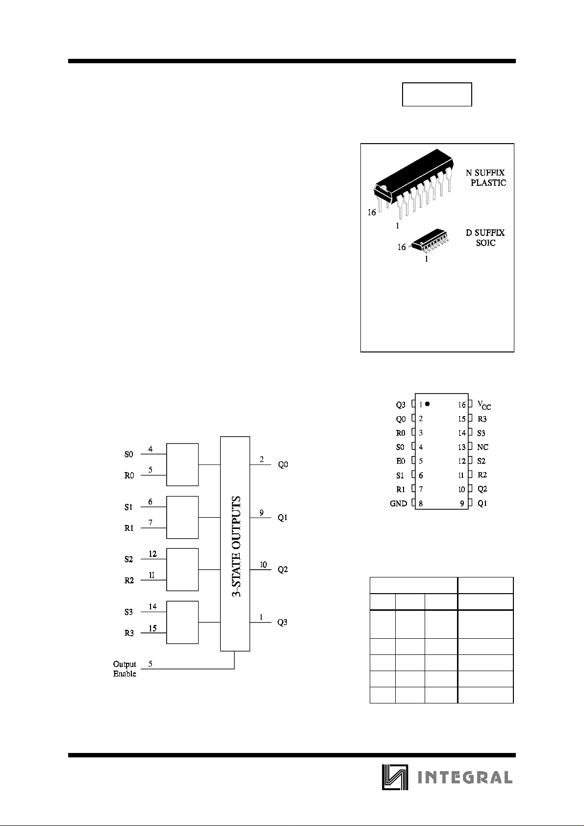
Quad 3-State R/S Latches
High-Voltage Silicon-Gate CMOS
The IW4043B types are quad cross-coupled 3-state CMOS NOR
latces. Each latch has a separate Q output and individual SET and
RESET inputs. The Q outputs are controlled by a common ENABLE
input. A logic “1” or high on the ENABLE input connects the latch
states to the Q outputs. A logic “0” or low on the ENABLE input
disconnects the latch states from the Q outputs, resulting in an open
circuit condition on the Q outputs. The open circuit feature allows
common busing of the outputs.
•
Operating Voltage Range: 3.0 to 18 V
•
Maximum input current of 1 µA at 18 V over full package-
temperature range; 100 nA at 18 V and 25°C
•
Noise margin (over full package temperature range):
1.0 V min @ 5.0 V supply
2.0 V min @ 10.0 V supply
2.5 V min @ 15.0 V supply
IW4043B
ORDERING INFORMATION
IW4043BN Plastic
IW4043BD SOIC
TA = -55° to 125° C for all packages
LOGIC DIAGRAM
PIN 13 = NO CONNECTION
PIN 16=V
PIN 8= GND
CC
PIN ASSIGNMENT
FUNCTION TABLE
Inputs Outputs
SROE Q
XX L High
Impedance
L L H No change
LH H L
HL H H
HH H H
X = don’t care
84
IW4043B
MAXIMUM RATINGS
*
Symbol Parameter Value Unit
V
CC
V
V
OUT
I
IN
P
P
DC Supply Voltage (Referenced to GND) -0.5 to +20 V
DC Input Voltage (Referenced to GND) -0.5 to VCC +0.5 V
IN
DC Output Voltage (Referenced to GND) -0.5 to VCC +0.5 V
DC Input Current, per Pin
Power Dissipation in Still Air, Plastic DIP+
D
SOIC Package+
Power Dissipation per Output Transistor 100 mW
D
±
10
750
500
Tstg Storage Temperature -65 to +150
T
Lead Temperature, 1 mm from Case for 10 Seconds
L
260
(Plastic DIP or SOIC Package)
*
Maximum Ratings are those values beyond which damage to the device may occur.
Functional operation should be restricted to the Recommended Operating Conditions.
+Derating - Plastic DIP: - 10 mW/°C from 65° to 125°C
SOIC Package: : - 7 mW/°C from 65° to 125°C
RECOMMENDED OPERATING CONDITIONS
Symbol Parameter Min Max Unit
V
VIN, V
T
CC
A
DC Supply Voltage (Referenced to GND) 3.0 18 V
DC Input Voltage, Output Voltage (Referenced to GND) 0 V
OUT
Operating Temperature, All Package Types -55 +125
CC
mA
mW
°
C
°
C
V
°
C
This device c ontains p rote ction ci rcuitr y to guard a gainst damage d ue to high st atic voltages or electr ic
fields. However, precautions must be taken to avoid applications of any voltage higher than maximum rated
voltages to this high-impedance circuit. For proper operation, V
GND≤(V
IN
or V
OUT
)≤VCC.
Unused inputs must always be tied to an appropriate logic voltage level (e.g., either GND or V
and V
IN
should be constrained to the range
OUT
CC
Unused outputs must be left open.
85
).

IW4043B
DC ELECTRICAL CHARACTERISTICS
(Voltages Referenced to GND)
Symbol Parameter Test Conditions V
V
V
V
IH
IL
OH
Minimum High-Level
Input Voltage
Maximum Low -Level
Input Voltage
Minimum High-Level
V
= 0.5 V or V
OUT
V
= 1.0 V or V
OUT
V
= 1.5 V or V
OUT
V
= 0.5 V or V
OUT
V
= 1.0 V or V
OUT
V
= 1.5 V or V
OUT
VIN=GND or V
CC
CC
CC
CC
CC
CC
CC
- 0.5V
- 1.0 V
- 1.5V
- 0.5V
- 1.0 V
- 1.5V
Output Voltage
V
OL
Maximum Low-Level
VIN=GND or V
CC
Output Voltage
I
IN
Maximum Input
VIN= GND or V
CC
Leakage Current
I
OZ
I
CC
Maximum Three State
Leakage Current
Maximum Qui escent
Output in High-Impedance
State
V
= GND or V
IN
V
= GND or V
OUT
VIN= GND or V
CC
CC
CC
Supply Current
(per Package)
I
OL
I
OH
Minimum Output Low
(Sink) Current
Minimum Output
High (Source) Current
VIN= GND or V
UOL=0.4 V
U
=0.5 V
OL
U
=1.5 V
OL
VIN= GND or V
UOH=2.5 V
U
=4.6 V
OH
U
=9.5 V
OH
U
=13.5 V
OH
CC
CC
V
5.0
10
15
5.0
10
15
5.0
10
15
5.0
10
15
18
18
5.0
10
15
20
5.0
10
15
5.0
5.0
10
15
CC
≥
14.95
-0.64
Guaranteed Limit
-55°C25°C
3.5
7
11
1.5
3
4
4.95
9.95
3.5
7
11
1.5
3
4
4.95
9.95
14.95
0.05
0.05
0.05
±
0.1
±
0.4
1
2
4
20
0.64
1.6
4.2
-2
0.05
0.05
0.05
±
0.1
±
0.4
1
2
4
20
0.51
1.3
3.4
-1.6
-0.51
-1.6
-4.2
-1.3
-3.4
≤
125
°
C
3.5
7
11
1.5
3
4
4.95
9.95
14.95
0.05
0.05
0.05
±
1.0
±
12.0
30
60
120
600
0.36
0.9
2.4
-1.15
-0.36
-0.9
-2.4
Unit
V
V
V
V
µ
A
µ
A
µ
A
mA
mA
86

IW4043B
AC ELECTRICAL CHARACTERISTICS
(CL=50pF, RL=200kΩ, Input tr=tf=20 ns)
Symbol Parameter V
t
PHL
, t
Maximum Propagation Delay, SET or RESET
PLH
to Q (Figure 1)
t
PHZ
, t
Maximum Propagation Delay, Output Enable to
PZH
Q (Figures 2,4)
t
PLZ
, t
Maximum Propagation Delay, Output Enable to
PZL
Q (Figures 2,4)
t
THL
, t
Maximum Output Transition Time, Any Output
TLH
(Figure 1)
C
IN
TIMING REQUIREMENTS
Maximum Input Capacitance - 7.5 pF
(CL=50pF, RL=200 kΩ, Input tr=tf=20 ns)
Symbol Parameter V
t
w
Minimum Pulse Width, SET or RESET (Figure3)5.0
V
5.0
10
15
5.0
10
15
5.0
10
15
5.0
10
15
V
10
15
CC
≥
CC
≥
Guaranteed Limit
-55°C25°C
300
140
100
230
110
80
180
100
70
200
100
80
300
140
100
230
110
80
180
100
70
200
100
80
Guaranteed Limit
-55°C25°C
160
80
40
160
80
40
≤
125°C
600
280
200
460
220
160
360
200
140
400
200
160
≤
125°C
320
160
80
Unit
ns
ns
ns
ns
Unit
ns
Figure 1. Switching Waveforms Figure 2. Switching Waveforms
Figure 3. Switching Waveforms
87

IW4043B
Figure 4. Test Circuit
TEST IN IN A
t
PHZVCC
t
GND V
PLZ
t
PZHVCC
t
GND V
PZL
GND GND
V
CC
GND GND
V
CC
CC
CC
EXPANDED LOGIC DIAGRAM
( 1/4 of the Device)
88
 Loading...