

Page 1
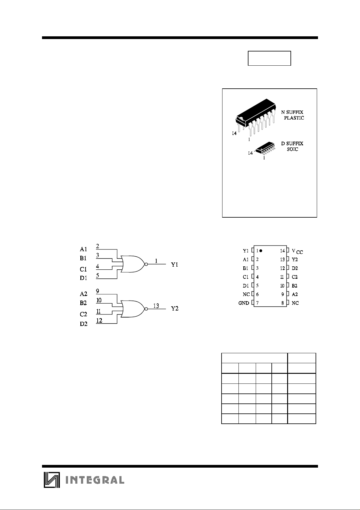
Dual 4-Input NOR Gate
High-Voltage Silicon-Gate CMOS
The IW4002B NOR gates provide the system designer with direct
emplementation of the NOR function.
•
Operating Voltage Range: 3.0 to 18 V
•
Maximum input current of 1 µA at 18 V over full packagetemperature range; 100 nA at 18 V and 25°C
•
Noise margin (over full package temperature range):
1.0 V min @ 5.0 V supply
2.0 V min @ 10.0 V supply
2.5 V min @ 15.0 V supply
TECHNICAL DATA
IW4002B
ORDERING INFORMATION
IW4002BN Plastic
IW4002BD SOIC
TA = -55° to 125° C for all packages
LOGIC DIAGRAM
PINS 6, 8 = NO CONNECTION
PIN 14 =V
PIN 7 = GND
CC
PIN ASSIGNMENT
NC = NO CONNECTION
FUNCTION TABLE
Inputs Output
ABCD Y
HXXX L
XHXX L
XXHX L
XXXH L
LLLL H
X = don’t care
7
Page 2
IW4002B
MAXIMUM RATINGS
*
Symbol Parameter Value Unit
V
CC
V
V
OUT
I
IN
P
P
DC Supply Voltage (Referenced to GND) -0.5 to +20 V
DC Input Voltage (Referenced to GND) -0.5 to VCC +0.5 V
IN
DC Output Voltage (Referenced to GND) -0.5 to VCC +0.5 V
DC Input Current, per Pin
Power Dissipation in Still Air, Plastic DIP+
D
SOIC Package+
Power Dissipation per Output Transistor 100 mW
D
±
10
750
500
Tstg Storage Temperature -65 to +150
T
Lead Temperature, 1 mm from Case for 10 Seconds
L
260
(Plastic DIP or SOIC Package)
*
Maximum Ratings are those values beyond which damage to the device may occur.
Functional operation should be restricted to the Recommended Operating Conditions.
+Derating - Plastic DIP: - 10 mW/°C from 65° to 125°C
SOIC Package: : - 7 mW/°C from 65° to 125°C
RECOMMENDED OPERATING CONDITIONS
Symbol Parameter Min Max Unit
V
VIN, V
T
CC
A
DC Supply Voltage (Referenced to GND) 3.0 18 V
DC Input Voltage, Output Voltage (Referenced to GND) 0 V
OUT
Operating Temperature, All Package Types -55 +125
CC
mA
mW
°
C
°
C
V
°
C
This device c ontains p rote ction ci rcuitr y to guard a gainst damage d ue to high st atic voltages or electr ic
fields. However, precautions must be taken to avoid applications of any voltage higher than maximum rated
voltages to this high-impedance circuit. For proper operation, V
GND≤(V
IN
or V
OUT
)≤VCC.
Unused inputs must always be tied to an appropriate logic voltage level (e.g., either GND or V
and V
IN
should be constrained to the range
OUT
CC
Unused outputs must be left open.
8
).
Page 3

IW4002B
DC ELECTRICAL CHARACTERISTICS
(Voltages Referenced to GND)
Symbol Parameter Test Conditions V
V
V
V
IH
IL
OH
Minimum High-Level
Input Voltage
Maximum Low -Level
Input Voltage
Minimum High-Level
V
=0.5V
OUT
V
=1.0 V
OUT
V
=1.5V
OUT
V
OUT
V
OUT
V
OUT
=0.5 V or V
=1.0 V or V
=1.5 V or V
CC
CC
CC
- 0.5 V
- 1.0 V
- 1.5 V
VIN=GND 5.0
Output Voltage
V
OL
Maximum Low-Level
VIN=GND or V
CC
Output Voltage
I
IN
Maximum Input
VIN= GND or V
CC
Leakage Current
I
CC
Maximum Qui escent
VIN= GND or V
CC
Supply Current
(per Package)
I
OL
I
OH
Minimum Output Low
(Sink) Current
Minimum Output
High (Source) Current
VIN= GND or V
UOL=0.4 V
U
=0.5 V
OL
U
=1.5 V
OL
VIN= GND or V
UOH=2.5 V
U
=4.6 V
OH
U
=9.5 V
OH
U
=13.5 V
OH
CC
CC
V
5.0
10
15
5.0
10
15
10
15
5.0
10
15
18
5.0
10
15
20
5.0
10
15
5.0
5.0
10
15
CC
Guaranteed Limit
≥
-55°C
3.5
7
11
1.5
3
4
4.95
9.95
14.95
14.95
0.05
0.05
0.05
±
0.1
0.25
0.5
1.0
5.0
0.64
1.6
4.2
-2.0
-0.64
-0.51
-1.6
-4.2
25
°
C
3.5
7
11
1.5
3
4
4.95
9.95
0.05
0.05
0.05
±
0.1
0.25
0.5
1.0
5.0
0.51
1.3
3.4
-1.6
-1.3
-3.4
≤
125
°
C
3.5
7
11
1.5
3
4
4.95
9.95
14.95
0.05
0.05
0.05
±
1.0
7.5
15
30
150
0.36
0.9
2.4
-1.15
-0.36
-0.9
-2.4
Unit
V
V
V
V
µ
A
µ
A
mA
mA
9
Page 4

IW4002B
AC ELECTRICAL CHARACTERISTICS
(CL=50pF, RL=200kΩ, Input tr=tf=20 ns)
Symbol Parameter V
t
PLH
, t
Maximum Propagation Delay, Input A, B,C
PHL
or D to Output Y (Figure 1)
t
TLH
, t
Maximum Output Transition Time, Any Output
THL
(Figure 1)
C
IN
Maximum Input Capacitance - 7.5 pF
V
5.0
10
15
5.0
10
15
CC
≥
Guaranteed Limit
-55°C25°C
250
120
90
200
100
80
250
120
90
200
100
80
≤
125°C
500
240
180
400
200
160
Unit
ns
ns
Figure 1. Switching Waveforms
EXPANDED LOGIC DIAGRAM
(1/2 of the Device)
10
 Loading...