

Page 1
Features:
n Extremely Rugged for Harsh Operating
Environments
n Over Temperature Protection
n Over Current Protection
n Active Drain to Source Clamp
n ESD Protection
n Compatible with standard POWER
MOSFET
n Low Operating Input Current
n Monolithic Construction
n Dual set/reset Threshold Input
IRSF3010
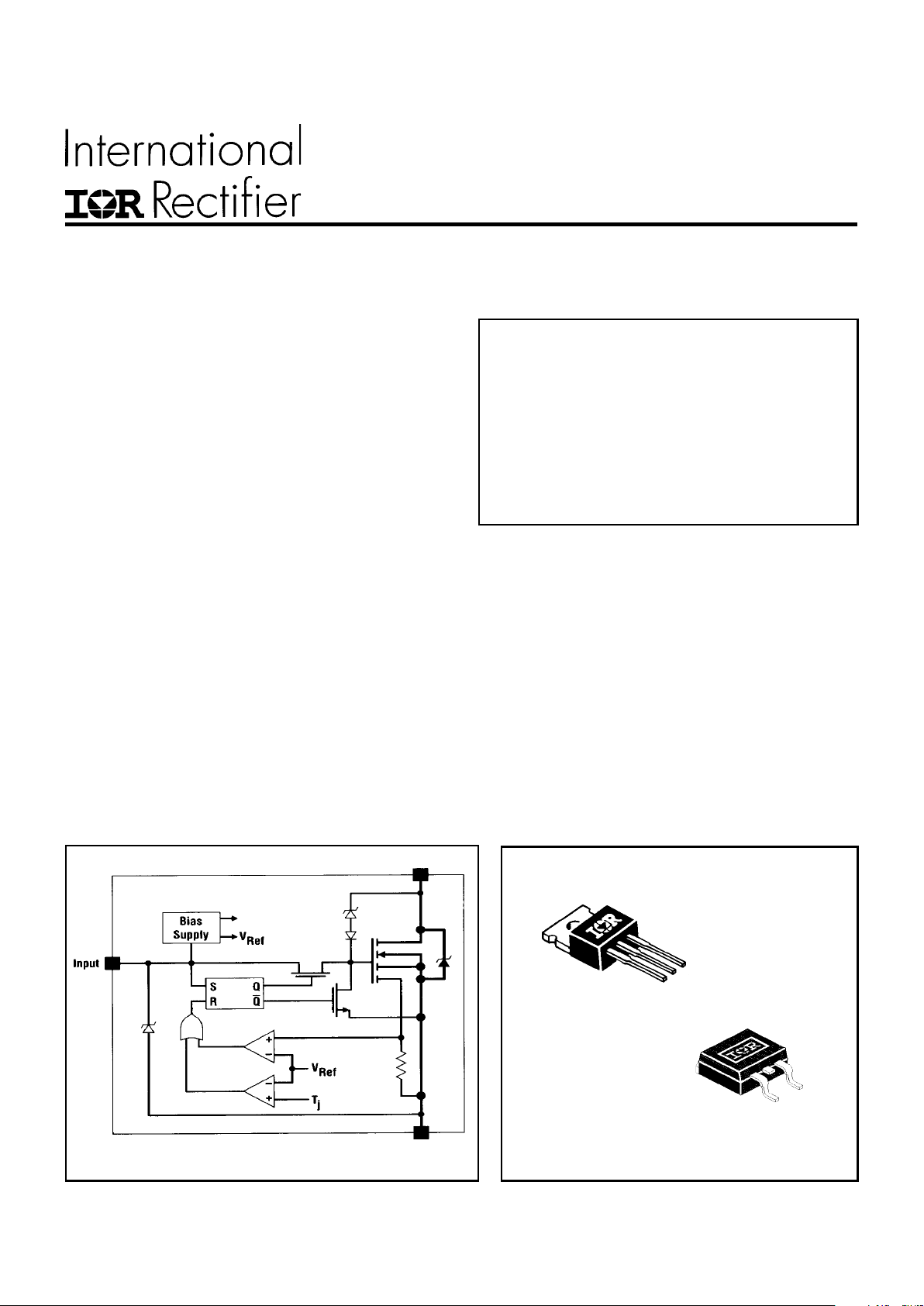
Available PackagesIRSF3010 - Block Diagram
V
ds(clamp)
50 V
R
ds(on)
80 m
ΩΩ
ΩΩ
Ω
I
ds(sd)
11 A
T
j(sd)
155 °C
E
AS
400 mJ
Source
Drain
Applications:
n DC Motor Drive
n Solenoid Driver
FULLY PROTECTED POWER MOSFET SWITCH
Pin Assignment
Pin 1 - Input
Pin 2 - Drain
Pin 3 - Source
Tab - Drain
Provisional Data Sheet No.PD-6.0027A
3
2
1
Tab
IRSF3010
IRSF3010S
Rating Summary:General Description:
The IRSF3010 is a three terminal monolithic
SMART POWER MOSFET with built in short circuit, over-temperature, ESD and over-voltage protections.
The on chip protection circuit latches off the
POWER MOSFET in case the drain current exceeds 14A (typical) or the junction temperature exceeds 165°C (typical) and keeps it off until the
input is driven low. The drain to source voltage
is actively clamped at 55V (typical), prior to the
avalanche of POWER MOSFET, thus improving
its performance during turn off with inductive
loads.
The input current requirements are very low
(300uA) which makes the IRSF3010 compatible with
most existing designs based on standard
POWER MOSFETs.
Page 2
IRSF3010
2
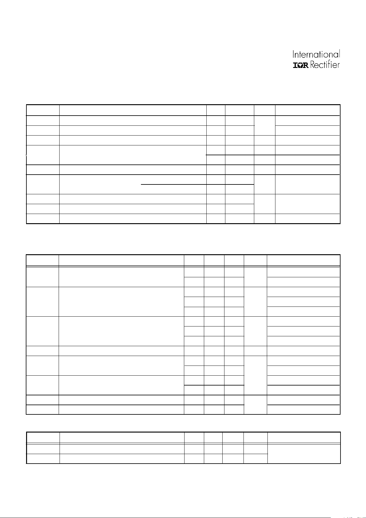
Absolute Maximum Ratings
Absolute Maximum Ratings indicate sustained limits beyond which damage to the device may occur. (Tc =
25°C unless otherwise specified.)
Symbol Parameter Definition Min. Max. Test Conditions
V
ds, max
Continuous Drain to Source Voltage — 50
V
in, max
Continuous Input Voltage -0.3 10
I
ds
Continuous Drain Current — self limited
P
d
Power Dissipation — 40 W T
c
≤ 25°C
Linear Derating Factor for Tc > 25°C — 0.33 W/°C
E
AS
Unclamped Single Pulse Inductive Energy — 40 0 m J
V
esd1
Electrostatic Discharge Voltage (Human Body Model) — 4000 1000pF . 1.5kΩ
V
esd2
(Machine Model) — 1000 200pF, 0Ω
T
Jop
Junction T emperature -55
self-limited
T
Stg
Storage T emperature -55 175
T
L
Lead T emperature (Soldering, 10 seconds) — 300
Thermal Characteristics
Units
V
V
o
C
Symbol Parameter Definition Min. Typ. Max. Units Test Conditions
V
ds,clamp
Drain to Source Clamp Voltage 50 54 — Ids = 10mA
—5662 Ids = 11A, tp = 700 µS
R
ds(on)
Drain to Source On Resistance — 70 80 Vin = 5V, Ids = 4A
—85— Vin = 4V, Ids = 4A
—53— Vin = 10V, Ids = 4A
I
dss
Drain to Source Leakage Current — — 10 Vds = 12V, Vin = 0V
— — 100 Vds = 50V, Vin = 0V
— 10 250 V
ds
=40V,Vin=0V,Tc=150oC
V
th
Input Threshold Voltage 1.5 2.0 2.5 V Vds = 5V, Ids = 1mA
I
i, on
Input Supply Current (Normal Operation) — 0.25 0.6 Vin = 5V
— 0.35 0.85 Vin = 10V
I
i, off
Input Supply Current (Protection Mode) — 0.5 1.0 Vin = 5V
—0.61.2 Vin = 10V
V
in, clamp
Input Clamp Voltage 10 10.8 — Iin = 10mA
V
sd
Body-Drain Diode Forward Drop ➁ — 1.2 1.5 Ids = -17A, Rin = 1k
Ω
Static Electrical Characteristics
(Tc = 25°C unless otherwise specified.)
V
mΩ
µA
mA
V
Symbol Parameter Definition Min. Typ. Max. Units Test Conditions
R
Θjc
Thermal Resistance, Junction to Case — 3.0 — °C/W
R
ΘjA
Thermal Resistance, Junction to Ambient — 60 — °C/W
Page 3
IRSF3010
3
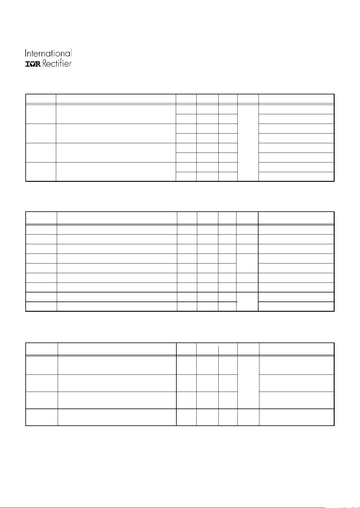
Notes:
1. EAS is tested with a constant current source of 11A applied for 700µS with Vin = OV and starting Tj = 25oC.
2. Input current must be limited to less than 5mA with a 1kΩ resistor in series with the input when the Body-Drain Diode
is forward biased.
Symbol Parameter Definition Min. Typ. Max. Units Test Conditions
V
ds,clamp
Temperature Coefficient of Drain to Source
Clamp Voltage — 18.2 —
V
th
Temperature Coefficient of Input Threshold
Voltage — -3.2 —
V
in,clamp
Temperature Coefficient of Input Clamp
Voltage — 7.0 —
I
ds(sd)
Temperature Coefficient of Over-Current
Shutdown Threshold — -21.5 — mA/oC
Ids = 10mA
Vds = 5V, Ids = 1mA
Iin = 10mA
Vin = 5V
mV/oC
T emperature Coefficients of Electrical Characteristics:
(Please see Figures 3 through 14 for more data on thermal characteristics of other electrical parameters.
Symbol Parameter Definition Min. Typ. Max. Units Test Conditions
t
don
Turn-On Delay time — 425 650 Vin = 5V
— 150 — Vin = 10V
t
r
Rise Time — 2000 4000 Vin = 5V
— 425 — Vin = 10V
t
doff
Turn-Off Delay time — 650 1000 Vin = 5V
— 850 — Vin = 10V
t
f
Fall Time — 500 800 Vin = 5V
— 450 — Vin = 10V
Switching Electrical Characteristics:
(Vcc = 14V, Resistive Load RL = 5Ω, Tc = 25 °C.) Please refer to Figure 15 for switching time definitions.
nS
Symbol Parameter Definition Min. Typ. Max. Units Test Conditions
I
ds(sd)
Over-Current Shutdown Threshold 11 14 17 A Vin = 5V
T
j(sd)
Over Temperature Shutdown Threshold 155 165 — °C Vin = 5V, Ids = 2A
V
protect
Minimum Input Voltage for Over-temp fxn. — 3 — V
t
Iresp
Over Current Response Time — 2 — See figure 16 for definition
t
Iblank
Over Current Blanking Time — 3 — See figure 16 for definition
I
peak
Peak Short Circuit Current — 2 0 — A See figure 16 for definition
V
reset
Protection Reset Voltage — 1.3 — V
t
reset
Protection Reset Time — 7 — See figure 17 for definition
t
Tresp OverTemperature Response Time
— 1 2 — See figure 18 for definition
µS
µS
Protection Characteristics:
(Tc = 25 °C unless otherwise specified.)
Page 4
IRSF3010
4
30
40
50
60
70
80
90
100
110
120
-50 -25 0 25 50 75 100 125 150
Temperature (°C)
Rds(on) (mOhm)
Vin = 10V
Vin = 5V
Ids = 4A
40
50
60
70
80
90
100
110
120
24681012141618
Ids (A)
Rds(on) (mOhm)
Vin = 4V
Vin = 5V
Vin = 7V
Vin = 10V
T = 25°C
Fig. 3 - On Resistance vs Drain to Source Current Fig. 4 - On Resistance vs. Temperature
13
14
15
16
17
45678910
Input Voltage (Volts)
Shut Down Current (A)
T = 25°C
Fig. 5 - Over-current Shutdown Threshold vs
Input Voltage
10
11
12
13
14
15
16
-50 -25 0 25 50 75 100 125 1 50
Temperature (°C)
Shut Down Current (A)
Vi n = 5V
Fig. 6 - Over-current Shutdown Threshold vs
Temperature
0
0.2
0.4
0.6
0.8
1
1.2
1.4
1.6
01234567891011
Input Volt age (Volt s )
Input Current (mA)
Iin ,off
T=25°C
Iin ,on
Rating
0
500
1000
1500
2000
2500
3000
3500
0255075100125150
Starting Ju nc tion Temperature (°C)
Single Pulse En ergy to Failur e (mJ)
Ids = 12A
Ids = 8A
Vdd = 25V
Figure 7 - Input Current vs. Input Voltage
Fig. 8 - Unclamped Single Pulse Inductive Energy to
Failure vs Starting Junction Temperature
Page 5

IRSF3010
5
F ig. 9 - Turn on characteristics vs Input Voltag e F ig. 10 - Turn on characteristics vs Temperat ure
Fig. 11 - Turn off characteristics vs Input Voltage Fig. 12 - Turn off characteristics vs Temperature
Fig. 13 - Source-Drain Diode Forward Voltage Fig. 14 - Transient Thermal Impedance, Junction to Case
0.00
0.50
1.00
1.50
2.00
2.50
34567891011
I
np ut Voltage ( Volt
s)
R
ise Time, On Delay (µ
S)
O
n Dela
y
R
ise Tim
e
T
= 25°
C
0.3
0.4
0.5
0.6
0.7
0.8
0.9
34567891011
I
np ut Voltage ( Volt
s)
F
all T i me, Off Delay (µ
S)
O
ff Dela
y
F
all Tim
e
T
= 25°
C
0.3
0.4
0.5
0.6
0.7
0.8
0.9
-50 -25 0 25 50 75 100 125 150
T
emperature (°C
)
F
all Time, Off Delay (µ
S)
O
ff Dela
y
F
a ll Tim
e
V
in = 5
V
1
10
100
0.6 0.8 1 1.2 1.4 1.6 1.8 2 2.2
S
ource to Drain Voltage (Volt
s)
R
everse Dra in C urrent (A
)
T
= 25°
C
T
= 150°
C
0.00
0.50
1.00
1.50
2.00
2.50
-50 -25 0 25 50 75 100 125 150
T
emperature (°C
)
R
ise Time, On Delay (µ
S)
O
n Dela
y
R
is e Tim
e
V
in = 5
V
0.01
0.1
1
10
1E-05 1E-04 1E-03 1E-02 1E-01 1E+00 1E+01
P
ulse Duration tp (
S)
T
hermal R esponse (°C/ W
)
0
.5
0.1
0
D
uty Fact o r
=
D
F=
0
.50
0
.20
0
.10
0
.05
0
.02
0
.01
0
.00
Page 6

IRSF3010
6
50%
90%
10%
V
ds
V
in
t
t
t
dontr
t
dofftf
I
ds
V
in
t
t
I
peak
t
I
blank
t
I
resp
Short applied
before turn-on
Short applied
after turn-on
5V
Vcc = 14V= 0
R
L
I
ds
V
in
t
t
5V
Vcc = 14V= 1 mHR
L
I
ds(sd)
t <
reset
t
t >
reset
t
I
ds
V
in
t
t
t
T
resp
5V
Vcc = 14V= 10
R
L
Ω
+ 5°C TJ= T
JSD
Fig. 15 - Definition of Switching times. Fig. 16 - Definition of I
peak
, t
Iblank
, t
Iresp
Fig. 17 - Definition of t
reset
Fig. 18 - Definition of t
Tresp
Page 7

IRSF3010
7
Case Outline TO-220AB (IRSF3010)
NOTES:
1. Dimensioning and tolerancing per ANSI Y14.5M, 1982
2. Controlling dimension: INCH
3. Dimensions shown are in millimeters (inches)
4. Conforms to JEDEC outline TO-251AA
5. Dimension does not include solder dip. Solder dip max. +0.16 (.006)
LEAD ASSIGNMENTS
1. Gate
2. Drain
3. Source
4. Drain
Page 8

IRSF3010
8
Case Outline SMD-220 (IRSF3010S)
Page 9

IRSF3010
9
Tape and Reel SMD-220 (IRSF3010S)
Page 10

IRSF3010
10
Application Information
Introduction
Protected monolithic POWER MOSFETs offer simple,
cost effective solutions in applications where extreme
operating conditions can occur. The margin between
the operating conditions and the absolute maximum values can be narrowed resulting in better
utilization of the device and lower cost. ESD protection also reduces the off-circuit failures during handling and assembly.
General Description
The IRSF3010 is a fully protected monolithic N-channel, logic level POWER MOSFET with 80mΩ (max)
on-resistance. The built-in protections include overcurrent, over-temperature, ESD and active over-voltage protections.
The over-current and over-temperature protection
makes the IRSF3010 indestructible at any load conditions in switching or in linear applications. The built-in
ESD protection minimizes the risk of ESD damage
when the device is off-circuit. The IRSF3010 is fully
characterized for avalanche operation and can be used
for fast de-energization of inductive loads.
The IRSF3010 Intelligent Power Switch that is
available in the TO220 package offers an easy upgrade from non-protected devices.
Block Diagram
The zener diode between the input and the source
(see figure 20) provides the ESD protection for the
input and also limits the applicable voltage to the input to 10V.
The R-S flip-flop memorizes the occurrence of an error condition and controls the Q2 and Q3 switches.
The flip-flop can be cleared by holding the input low
for the specified minimum duration.
COMP1 and COMP2 comparators are used to compare the over-current and over-temperature signals
with the built-in reference. Either comparator can reset the fault flip-flop and turn Q1 off. During fault condition, Q2 disconnects gate of Q1 from the input, Q3
shorts the gate and source of Q1, resulting in rapid
turn-off of Q1. The zener diode between the gate and
drain of Q1 turns Q1 on, when the drain to source
voltage exceeds 55V.
Switching Characteristics
In the IRSF3010 the control logic and the protection
circuits are powered from the input pin. When positive voltage appears at the input pin the R-S flip-flop
turns Q2 on and connects the gate of the main device
to the input.
The turn-on speed is limited by the channel resistance
of Q2 and the gate charge requirements of Q1. The
typical switching waveforms at 5V input voltage are
shown in figure 21. Using higher input voltage will
improve the turn-on time but it does not affect the turnoff switching speed.
Fig.20 Block Diagram
Fig.21 Waveforms switching clamped indictive
load using 5V input voltage
Input voltage 5V/
Drain Current: 1A/div .
Drain voltage 5V/
Time: 1µsV/div.
Page 11

IRSF3010
11
The typical waveforms at 7V input voltage are shown
in figure 22. In typical switching applications, below
40kHz, the difference in switching losses between the
IRSF3010 and the same size standard MOSFET is
negligible.
Fig. 22 Switching waveforms with 7V Input
voltage
The typical waveforms at over-current shut-down are
shown in figure 23. After turn-on the current in the
inductor at the drain starts ramping up. At about 1 5A
the over-current protection shuts down the device.
Over-temperature Protection
Figure 24 illustrates the operation of the over-temperature protection. The IRSF3010 switches a 1Ω resistive load to a 12V power supply. When the thermal
balance is established the junction temperature is limited on pulse by pulse basis.
Fig. 24 Over-temperature shut-down
Fig. 23 Waveforms at over-current shut-down
Over-voltage Protection
When the drain to source voltage exceeds 55V the
zener diode between gate and drain turns the
IRSF3010 on, before the breakdown voltage of the
drain-source diode is reached. This greatly enhances
the energy the device can withstand safely during turnoff of inductive loads compared to avalanche breakdown. Thus the device can be used for fast deenergization of inductive loads. The absorbed energy
is limited only by the maximum junction temperature.
Over-current Protection
When the drain current exceeds the preset limit the
protection circuit resets the internal flip-flop and turns
Q1 off. The normal operation can be restored by holding the input voltage below the specified threshold level
(approx. 1.3V) for the specified minimum t
reset
time.
Input voltage 10V/div.
Drain voltage 5V/div .
Drain Current: 2A/div.
Time: 10µsV/div .
Time: 10µsV/div .
Drain Current: 2A/div .
Input voltage 5V/div.
Drain voltage 5V/div.
Input voltage 5V/
Drain voltage 5V/
Drain Current: 1A/
Time: 1µsV/div.
WORLD HEADQUARTERS: 233 Kansas St., El Segundo, California 90245, Tel: (310) 322 3331
EUROPEAN HEADQUARTERS: Hurst Green, Oxted, Surrey RH8 9BB, UK Tel: ++ 44 1883 732020
IR CANADA: 7321 Victoria Park Ave., Suite 201, Markham, Ontario L3R 2Z8, Tel: (905) 475 1897
IR GERMANY: Saalburgstrasse 157, 61350 Bad Homburg Tel: ++ 49 6172 96590
IR ITALY: Via Liguria 49, 10071 Borgaro, Torino Tel: ++ 39 11 451 0111
IR FAR EAST: 171 (K&H Bldg.), 30-4 Nishi-ikebukuro 3-Chome, Toshima-ku, Tokyo Japan Tel: 81 3 3983 0086
IR SOUTHEAST ASIA: 315 Outram Road, #10-02 Tan Boon Liat Building, Singapore 0316 Tel: 65 221 8371
http://www.irf.com/ Data and specifications subject to change without notice. 12/96
 Loading...