

查询IRLML2402供应商
PD- 93755
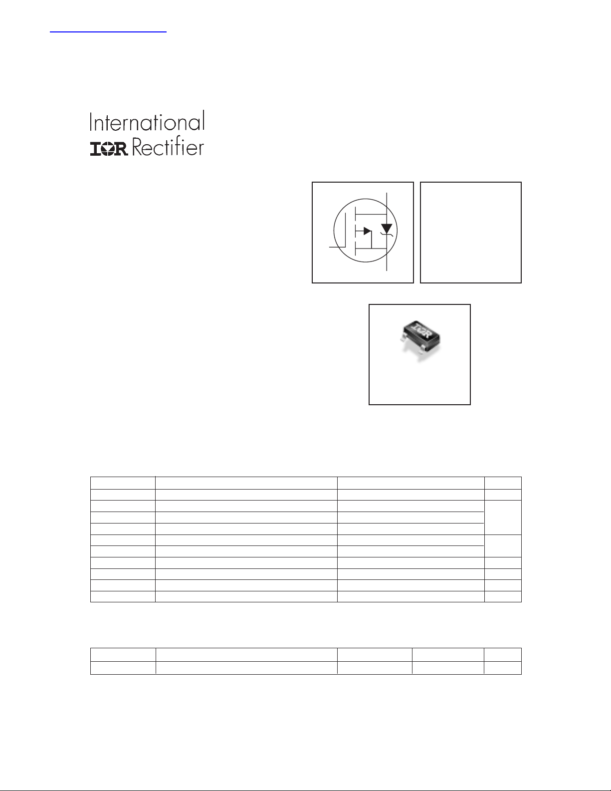
IRLML6402
HEXFET® Power MOSFET
l Ultra Low On-Resistance
l P-Channel MOSFET
l SOT-23 Footprint
l Low Profile (<1.1mm)
l Available in Tape and Reel
l Fast Switching
G
D
V
= -20V
DSS
R
S
DS(on)
= 0.065Ω
Description
These P-Channel MOSFETs from International Rectifier utilize
advanced processing techniques to achieve extremely low onresistance per silicon area. This benefit, combined with the fast
switching speed and ruggedized device design that HEXFET
power MOSFETs are well known for, provides the designer with
an extremely efficient and reliable device for use in battery and
load management.
A thermally enhanced large pad leadframe has been incorporated
Micro3
into the standard SOT-23 package to produce a HEXFET Power
MOSFET with the industry's smallest footprint. This package,
dubbed the Micro3, is ideal for applications where printed
circuit board space is at a premium. The low profile (<1.1mm)
of the Micro3 allows it to fit easily into extremely thin application
environments such as portable electronics and PCMCIA cards.
The thermal resistance and power dissipation are the best
available.
Absolute Maximum Ratings
Parameter Max. Units
V
DS
ID @ TA = 25°C Continuous Drain Current, VGS @ -4.5V -3.7
ID @ TA= 70°C Continuous Drain Current, VGS @ -4.5V -2.2 A
I
DM
PD @TA = 25°C Power Dissipation 1.3
PD @TA = 70°C Power Dissipation 0.8
E
AS
V
GS
T
J, TSTG
Drain- Source Voltage -20 V
Pulsed Drain Current -22
Linear Derating Factor 0.01 W/°C
Single Pulse Avalanche Energy 11 mJ
Gate-to-Source Voltage ± 12 V
Junction and Storage Temperature Range -55 to + 150 °C
W
Thermal Resistance
Parameter Typ. Max. Units
R
θJA
Maximum Junction-to-Ambient 75 100 °C/W
www.irf.com 1
8/13/99
IRLML6402
Electrical Characteristics @ TJ = 25°C (unless otherwise specified)
Parameter Min. Typ. Max. Units Conditions
V
(BR)DSS
∆V
(BR)DSS
R
DS(on)
V
GS(th)
g
fs
I
DSS
I
GSS
Q
g
Q
gs
Q
gd
t
d(on)
t
r
t
d(off)
t
f
C
iss
C
oss
C
rss
Drain-to-Source Breakdown Voltage -20 ––– ––– V VGS = 0V, ID = -250µA
/∆T
Breakdown Voltage Temp. Coefficient ––– -0.009 ––– V/°C Reference to 25°C, ID = -1mA
J
Static Drain-to-Source On-Resistance
––– 0.050 0.065 VGS = -4.5V, ID = -3.7A
––– 0.080 0.135 VGS = -2.5V, ID = -3.1A
Ω
Gate Threshold Voltage -0.40 -0.55 -0.95 V VDS = VGS, ID = -250µA
Forward Transconductance 6.0 ––– ––– S VDS = -10V, ID = -3.7A
Drain-to-Source Leakage Current
Gate-to-Source Forward Leakage ––– ––– -100 VGS = -12V
Gate-to-Source Reverse Leakage ––– ––– 100 VGS = 12V
––– ––– -1.0 VDS = -20V, VGS = 0V
––– ––– -25 VDS = -20V, VGS = 0V, TJ = 70°C
µA
nA
Total Gate Charge ––– 8.0 12 ID = -3.7A
Gate-to-Source Charge ––– 1.2 1.8 nC VDS = -10V
Gate-to-Drain ("Miller") Charge ––– 2.8 4.2 VGS = -5.0V
Turn-On Delay Time ––– 350 –– – VDD = -10V
Rise Time ––– 48 ––– ID = -3.7A
Turn-Off Delay Time ––– 588 ––– RG = 89Ω
ns
Fall Time ––– 381 ––– RD = 2.7Ω
Input Capacitance ––– 633 ––– VGS = 0V
Output Capacitance –– – 145 ––– pF VDS = -10V
Reverse Transfer Capacitance ––– 110 ––– ƒ = 1.0MHz
Source-Drain Ratings and Characteristics
Parameter Min. Typ. Max. Units Conditions
I
S
I
SM
V
SD
t
rr
Q
rr
Continuous Source Current MOSFET symbol
(Body Diode)
Pulsed Source Current integral reverse
(Body Diode)
––– –––
––– –––
-1.3
-22
showing the
A
p-n junction diode.
G
Diode Forward Voltage ––– ––– -1.2 V TJ = 25°C, IS = -1.0A, VGS = 0V
Reverse Recovery Time ––– 29 43 n s TJ = 25°C, IF = -1.0A
Reverse RecoveryCharge ––– 11 17 nC di/dt = -100A/µs
Notes:
Repetitive rating; pulse width limited by
max. junction temperature.
Pulse width ≤ 300µs; duty cycle ≤ 2%.
Surface mounted on 1" square single layer 1oz. copper FR4 board,
steady state.
Starting T
RG = 25Ω, I
= 25°C, L = 1.65mH
J
= -3.7A.
AS
** For recommended footprint and soldering techniques refer to application note #AN-994.
2 www.irf.com
D
S
IRLML6402
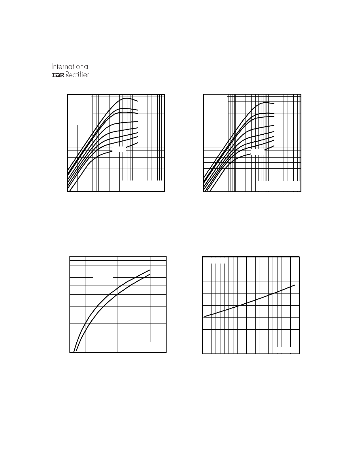
100
10
TOP
BOTTOM
VGS
-7.00V
-5.00V
-4.50V
-3.50V
-3.00V
-2.70V
-2.50V
-2.25V
-2.25V
D
-I , Drain-to-Source Current (A)
20µs PULSE WIDTH
°
T = 25 C
1
0.1 1 10 100
-V , Drain-to-Source Voltage (V)
DS
100
J
100
10
TOP
BOTTOM
VGS
-7.00V
-5.00V
-4.50V
-3.50V
-3.00V
-2.70V
-2.50V
-2.25V
-2.25V
D
-I , Drain-to-Source Current (A)
20µs PULSE WIDTH
1
0.1 1 10 100
-V , Drain-to-Source Voltage (V)
DS
T = 150 C
°
J
Fig 2. Typical Output CharacteristicsFig 1. Typical Output Characteristics
2.0
I =
D
-3.7A
°
T = 25 C
J
°
T = 150 C
J
1.5
1.0
(Normalized)
D
-I , Drain-to-Source Current (A)
V = -15V
DS
10
2.0 3.0 4.0 5.0 6.0 7.0 8.0
-V , Gate-to-Source Voltage (V)
GS
20µs PULSE WIDTH
Fig 3. Typical Transfer Characteristics
0.5
DS(on)
R , Drain-to-Source On Resistance
0.0
-60 -40 -20 0 20 40 60 80 100 120 140 160
T , Junction Temperature ( C)
J
Fig 4. Normalized On-Resistance
V =
GS
°
-4.5V
Vs. Temperature
www.irf.com 3

IRLML6402
1000
800
V
= 0V, f = 1 MHZ
GS
C
= C
iss
gs
C
= C
rss
gd
C
= C
ds
+ C
oss
+ Cgd, C
gd
Ciss
600
400
C, Capacitance(pF)
200
Coss
Crss
0
1 10 100
VDS, Drain-to-Source Voltage (V)
Fig 5. Typical Capacitance Vs.
Drain-to-Source Voltage
100
SHORTED
ds
10
I =
-3.7A
D
V = -10V
8
6
4
2
GS
-V , Gate-to-Source Voltage (V)
0
0 3 6 9 12
Q , Total Gate Charge (nC)
G
DS
FOR TEST CIRCUIT
SEE FIGURE
Fig 6. Typical Gate Charge Vs.
Gate-to-Source Voltage
100
OPERATION IN THIS AREA LIMITED
BY R
DS(on)
13
10us
100us
1ms
10ms
10
°
T = 150 C
J
1
°
T = 25 C
J
SD
-I , Reverse Drain Current (A)
V = 0 V
0.1
0.2 0.4 0.6 0.8 1.0 1.2
-V ,Source-to-Drain Voltage (V)
SD
GS
Fig 7. Typical Source-Drain Diode
10
1
D
-I , Drain Current (A)I , Drain Current (A)
°
= 25 C
C
T T= 150 C
Single Pulse
0.1
0.1 1 10 100
°
J
-V , Drain-to-Source Voltage (V)
DS
Fig 8. Maximum Safe Operating Area
Forward Voltage
4 www.irf.com

IRLML6402
(
)
4.0
3.0
2.0
D
-I , Drain Current (A)
1.0
0.0
25 50 75 100 125 150
T , Case Temperature ( C)
C
°
Fig 9. Maximum Drain Current Vs.
Case Temperature
1000
25
TOP
20
15
10
5
AS
E , Single Pulse Avalanche Energy (mJ)
0
25 50 75 100 125 150
Starting T , Junction Temperature ( C)
J
BOTTOM
Fig 10. Maximum Avalanche Energy
Vs. Drain Current
I
D
-1.7A
-3.0A
-3.7A
°
100
thJA
D = 0.50
0.20
0.10
10
0.05
0.02
0.01
1
Thermal Response (Z )
0.1
0.00001 0.0001 0.001 0.01 0.1 1 10
SINGLE PULSE
THERMAL RESPONSE
Notes:
1. Duty factor D = t / t
2. Peak T = P x Z + T
t , Rectangular Pulse Duration (sec)
1
J DM thJA A
1 2
P
DM
t
1
t
2
Fig 11. Maximum Effective Transient Thermal Impedance, Junction-to-Ambient
www.irf.com 5

IRLML6402
0.14
)
Ω
0.12
0.10
0.08
)
0.20
Ω
VGS = -2.5V
0.16
0.12
0.06
, Drain-to -Source Voltage (
0.04
DS(on)
R
0.02
2.0 3.0 4.0 5.0 6.0 7.0
-V
Gate -to -Source Voltage ( V )
GS,
Id = -3.7A
Fig 12. Typical On-Resistance Vs.
Gate Voltage
0.08
, Drain-to-Source On Resistance (
0.04
DS ( on )
0.00
R
0 5 10 15 20 25 30
-ID , Drain Current ( A )
Fig 13. Typical On-Resistance Vs.
Drain Current
VGS = -4.5V
6 www.irf.com

Package Outline
(
)
(
)
(
)
)
(
)
Micro3
Dimensions are shown in millimeters (inches)
D
3
- B -
3
E
- A -
- C B 3X
0.10 (.004) M C A S B S
NOTES:
1. DIMENSIO NING & TO LE RA NC ING P ER AN SI Y14.5M-1982.
2. CONTROLLING DIMENSION : INCH.
DIMENSIONS DO NOT INCLUDE MO LD FLASH.
3
3
1
2
e
e1
A
A1
LEAD ASSIGNMENTS
1 - GAT E
2 - SOURCE
3 - DRA IN
H
.008 ) M A M
0.20
0.008
.003
θ
L
3X 3X
IRLML6402
INC H E S MILLIM ET E RS
DIM
MIN MAX MIN MAX
A .03 2 .044 0.82 1.11
A1 .001 .004 0.02 0.10
B .01 5 .021 0.38 0.54
C .004 .006 0.10 0.15
D .105 .120 2.67 3.05
e .0750 BASIC 1.90 BASIC
e1 .0375 BAS IC 0.95 BAS IC
E .047 .055 1.20 1.40
H .083 .098 2.10 2.50
L .005 .010 0.13 0.25
θ
0° 8° 0° 8°
MINIMUM RECOM MENDED FOO TPRINT
C
0.90
.035
3X
0.80 ( .031
3X
2.00
.079
0.95 ( .037
2X
Part Marking Information
Micro3
EXAM PLE : THIS IS AN IRLM L6302
WORK
PART NUMBER
1 C YW
Y = YEAR CODE
W = W EEK CODE
PART NU MBER EXAM PLES:
1A = IRLML2402
1B = IRLML2803
1C = IRLM L6302
1D = IRLM L5103
DATE
CODE
TOP
DATE CODE EXAMPLES:
YW W = 9503 = 5C
YW W = 9532 = EF
YEAR Y WEEK W
2001 1 01 A
2002 2 02 B
2003 3 03 C
1994 4 04 D
1995 5
1996 6
1997 7
1998 8
1999 9
2000 0 24 X
25 Y
26 Z
W O R K WEEK = (1-26) IF PRECEDED BY LAST DIGIT OF CALENDER YEAR
W O R K WEEK = ( 27-52) IF PRECEDED BY LETTER
WORK
YEAR Y WEEK W
2001 A 27 A
2002 B 28 B
2003 C 29 C
1994 D 30 D
1995 E
1996 F
1997 G
1998 H
1999 J
2000 K 50 X
51 Y
52 Z
www.irf.com 7

IRLML6402
Tape & Reel Information
Micro3
Dimensions are shown in millimeters (inches)
2.05 ( .080 )
1.95 ( .077 )
TR
FEED DIRECTION
178.00
( 7.008 )
MA X.
4.1 ( .161 )
3.9 ( .154 )
4.1 ( .161 )
3.9 ( .154 )
1.6 ( .062 )
1.5 ( .060 )
1.1 ( .043 )
0.9 ( .036 )
1.85 ( .072 )
1.65 ( .065 )
3.55 ( .139 )
3.45 ( .136 )
1.32 ( .051 )
1.12 ( .045 )
8.3 ( .326 )
7.9 ( .312 )
0.35 ( .013 )
0.25 ( .010 )
9.90 ( .390 )
8.40 ( .331 )
NOTES:
1. CON TROLLING DIMENSION : MILLIMETER.
2. OU T LINE C ONF O R M S T O E IA-481 & E IA-541.
WORLD HEADQUARTERS: 233 Kansas St., El Segundo, California 90245, Tel: (310) 322 3331
IR GREAT BRITAIN: Hurst Green, Oxted, Surrey RH8 9BB, UK Tel: ++ 44 1883 732020
IR CANADA: 15 Lincoln Court, Brampton, Ontario L6T3Z2, Tel: (905) 453 2200
IR GERMANY: Saalburgstrasse 157, 61350 Bad Homburg Tel: ++ 49 6172 96590
IR ITALY: Via Liguria 49, 10071 Borgaro, Torino Tel: ++ 39 11 451 0111
IR FAR EAST: K&H Bldg., 2F, 30-4 Nishi-Ikebukuro 3-Chome, Toshima-Ku, Tokyo Japan 171 Tel: 81 3 3983 0086
IR SOUTHEAST ASIA: 1 Kim Seng Promenade, Great World City West Tower, 13-11, Singapore 237994 Tel: ++ 65 838 4630
IR TAIWAN:16 Fl. Suite D. 207, Sec. 2, Tun Haw South Road, Taipei, 10673, Taiwan Tel: 886-2-2377-9936
http://www.irf.com/ Data and specifications subject to change without notice. 8/99
8 www.irf.com
 Loading...