

Page 1
HEXFET
Next Data SheetIndex
Previous Datasheet
To Order
®
TRANSIST OR
Provisional Data Sheet No. PD-9.2002
IRFV260
N-CHANNEL
200 Volt, 0.060
ΩΩ
Ω, HEXFET
ΩΩ
HEXFET technology is the key to International
Rectifier’s advanced line of power MOSFET transistors. The efficient geometry design achieves very
low on-state resistance combined with high transconductance.
HEXFET transistors also feature all of the well-established advantages of MOSFETs, such as voltage
control, very fast switching, ease of paralleling and
electrical parameter temperature stability. They are
well-suited for applications such as switching power
supplies, motor controls, inverters, choppers, audio
amplifiers, high energy pulse circuits and virtually
any application where high reliability is required.
The HEXFET transistor’s totally isolated package
eliminates the need for additional isolating material
between the device and the heatsink. This improves
thermal efficiency and reduces drain capacitance.
Absolute Maximum Ratings
Parameter IRFV260 Units
ID @ VGS = 10V, TC = 25°C Continuous Drain Current 45*
ID @ VGS = 10V, TC = 100°C Continuous Drain Current 29
I
DM
PD @ TC = 25°C Max. Power Dissipation 300 W
V
GS
E
AS
I
AR
E
AR
dv/dt Peak Diode Recovery dv/dt 4.3
T
J
T
STG
* ID current limited by pin diameter
Pulsed Drain Current 180
Linear Derating Factor 2.4 W/K
Gate-to-Source Voltage ±20 V
Single Pulse Avalanche Energy 700 m J
Avalanche Current 45 A
Repetitive Avalanche Energy 30 m J
Operating Junction -55 to 150
Storage Temperature Range
Lead Temperature 300 (0.063 in. (1.6mm) from case for 10 sec.)
Weight 10.9 (typical) g
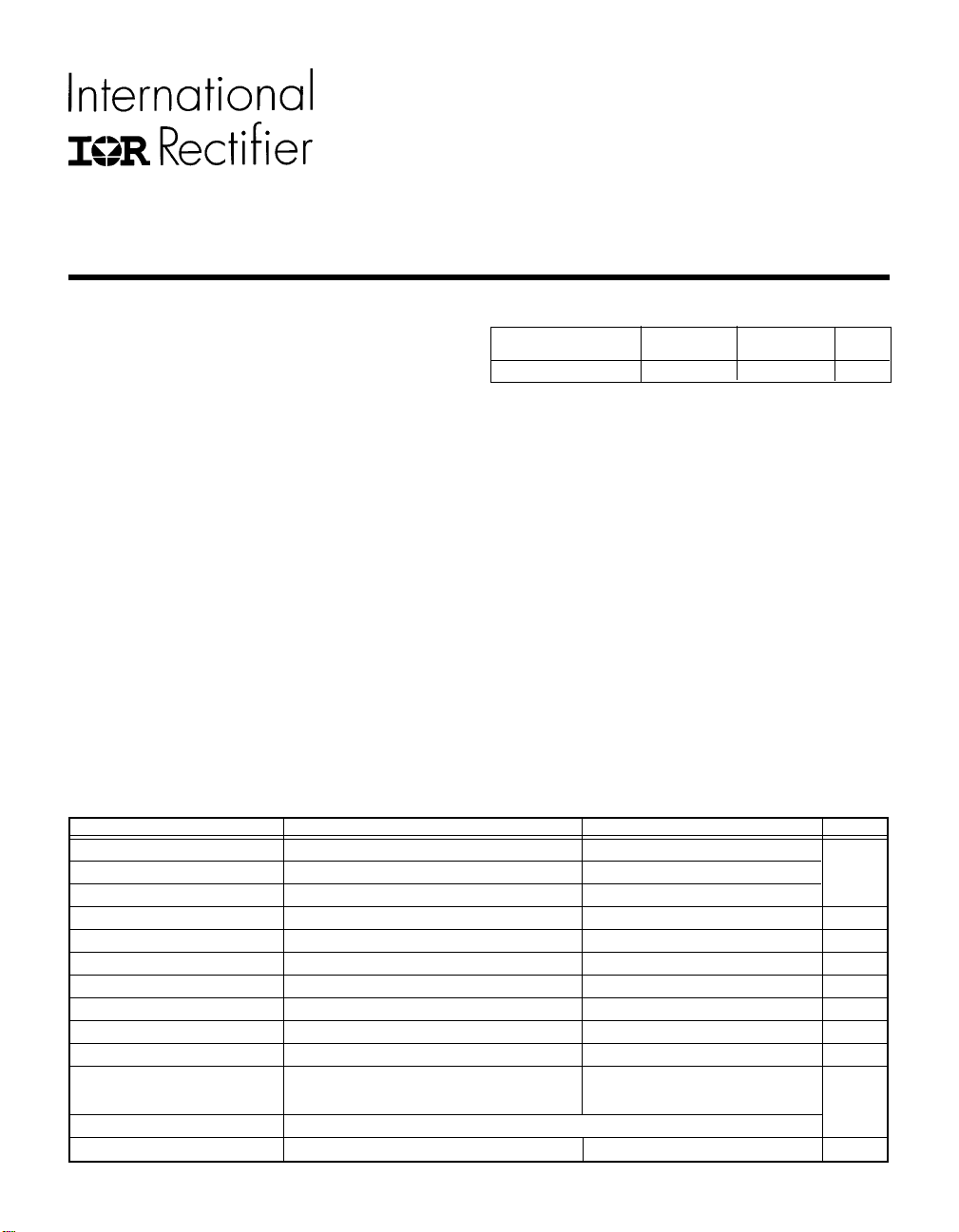
Product Summary
Part Number BVDSS RDS(on) ID
IRFV260 200V 0.060Ω 45A*
Features:
n Hermetically Sealed
n Electrically Isolated
n Simple Drive Requirements
n Ease of Paralleling
n Ceramic Eyelets
A
V/ns
o
C
Page 2
IRFV260 Device
Next Data SheetIndex
Previous Datasheet
To Order
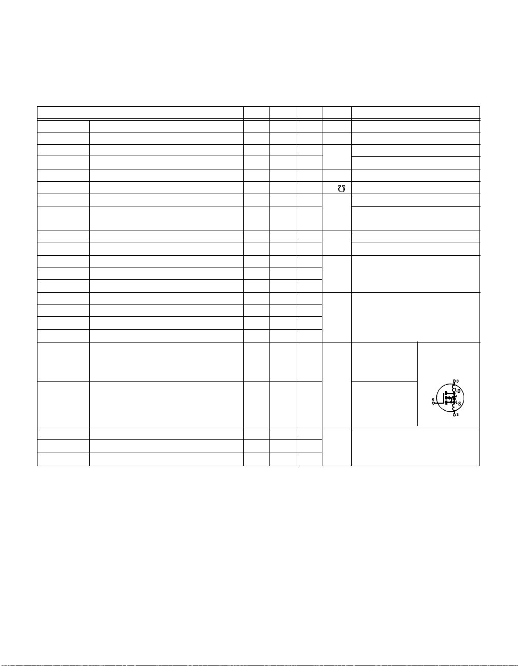
Electrical Characteristics @ Tj = 25°C (Unless Otherwise Specified)
Parameter Min. Typ. Max. Units Test Conditions
BV
DSS
∆BV
R
DS(on)
V
GS(th)
g
fs
I
DSS
I
GSS
I
GSS
Q
g
Q
gs
Q
gd
t
d(on)
t
r
t
d(off)
t
f
L
D
L
S
DSS
Drain-to-Source Breakdown Voltage 200 — — V VGS = 0V, ID = 1.0 mA
/∆TJTemp. Coefficient of Breakdown Voltage — 0.24 — V/°C Reference to 25°C, ID = 1.0 mA
Static Drain-to-Source — — 0.060 VGS = 10V, ID =29A
On-State Resistance — — 0.068
Gate Threshold Voltage 2.0 — 4.0 V VDS = VGS, ID = 250µA
Forward Transconductance 22 — — S ( )VDS ≥ 15V, IDS = 29A
Zero Gate Voltage Drain Current — — 25
— — 250 VDS = 0.8 x Max Rating
Gate-to-Source Leakage Forward — — 100
Gate-to-Source Leakage Reverse — — -100 VGS = -20V
Total Gate Charge — — 230 VGS =10V, ID = 45A
Gate-to-Source Charge — — 40 nC VDS = Max. Rating x 0.5
Gate-to-Drain (“Miller”) Charge — — 110
Tu rn-On Delay Time — — 29 VDD = 100V, ID =45A,
Rise Time — — 120 ns RG = 2.35Ω, VGS =10V
Tur n-Off Delay Time — — 110
Fall Time — — 92
Internal Drain Inductance — 8.7 —
Internal Source Inductance — 8.7 —
Ω
VDS=0.8 x Max Rating,VGS=0V
µA
nA
Measured from the
drain lead, 6mm (0.25
in.) from package to
center of die.
Measured from the
nH
source lead, 6mm
(0.25 in.) from package
to source bonding pad.
VGS = 10V, ID = 45A
VGS = 0V, TJ = 125°C
VGS = 20V
Modified MOSFET
symbol showing the
internal inductances.
C
C
C
iss
oss
rss
Input Capacitance — 5100 — VGS = 0V, VDS = 25V
Output Capacitance — 1100 — pF f = 1.0 MHz
Reverse Transfer Capacitance — 280 —
Page 3

IRFV260 Device
To Order
Next Data SheetIndex
Previous Datasheet
Source-Drain Diode Ratings and Characteristics
Parameter Min. Typ. Max. Units Test Conditions
I
Continuous Source Current (Body Diode) — — 45* Modified MOSFET symbol showing the
S
I
Pulse Source Current (Body Diode) — — 180 A integral rev erse p-n junction rectifier.
SM
V
Diode Forward Voltage — — 1.8 V Tj = 25°C, IS = 45A, VGS = 0V
SD
t
Reverse Recovery Time — — 420 ns Tj = 25°C, IF = 45A, di/dt ≤ 100A/µs
rr
QRRReverse Recovery Charge — — 4.9 µCV
t
Forward Turn-On Time
on
Intrinsic turn-on time is negligible. Turn-on speed is substantially controlled by LS + LD.
≤ 50V
DD
Thermal Resistance
Parameter Min. Typ. Max. Units Test Conditions
R
R
R
thJC
thJA
thCS
Junction-to-Case — — 0.42
Junction-to-Ambient — — 30
Case-to-Sink — 0.21 — mounting surface flat, smooth
K/W
typical socket mount
Repetitive Rating; Pulse width limited by
maximum junction temperature.
@ V
= 50V, Star ting TJ = 25°C,
DD
EAS = [0.5 * L * (I
Peak IL = 45A, VGS = 10V, 25 ≤ RG ≤ 200Ω
2
) * [BV
L
DSS
/(BV
DSS-VDD
I
≤ 45A, di/dt ≤ 130 A/ µs,
SD
VDD ≤ BV
Suggested RG = 2.35Ω
)]
Pulse width ≤ 300 µs; Duty Cycle ≤ 2%
K/W = °C/W
W/K = W/°C
, TJ ≤ 150°C
DSS
Page 4

Case Outline and Dimensions — T O-258AA
To Order
Next Data SheetIndex
Previous Datasheet
IRFV260 Device
NOTES:
1. Dimensioning and tolerancing per ANSI Y14.5M - 1982.
2. All dimensions in millimeters (inches)
BERYLLIA WARNING PER MIL-PRF-19500
Packages containing beryllia shall not be ground, sandblasted,
machined, or have other operations performed on them which will
produce beryllia or beryllium dust. Furthermore, beryllium oxides
packages shall not be placed in acids that will produce fumes
containing beryllium.
IR FAR EAST: K&H Bldg., 2F, 3-30-4 Nishi-Ikeburo 3-Chome, Toshima-Ki, Tokyo Japan 171 Tel: 81 3 3983 0086
IR SOUTHEAST ASIA: 315 Outram Road, #10-02 Tan Boon Liat Building, Singapore 0316 Tel: 65 221 8371
CAUTION
WORLD HEADQUARTERS: 233 Kansas St., El Segundo, California 90245, Tel: (310) 322 3331
EUROPEAN HEADQUARTERS: Hurst Green, Oxted, Surrey RH8 9BB, UK Tel: ++ 44 1883 732020
IR CANADA: 7321 Victoria Park Ave., Suite 201, Markham, Ontario L3R 2Z8, Tel: (905) 475 1897
IR GERMANY: Saalburgstrasse 157, 61350 Bad Homburg Tel: ++ 49 6172 96590
http://www.irf.com/ Data and specifications subject to change without notice. 7/96
LEGEND:
1. Drain
2.. Source
3. Gate
IR ITALY: Via Liguria 49, 10071 Borgaro, Torino Tel: ++ 39 11 451 0111
 Loading...