

Page 1
PD- 9.1336A
PRELIMINARY
IRFR/U024N
HEXFET® Power MOSFET
l Ultra Low On-Resistance
l Surface Mount (IRFR024N)
l Straight Lead (IRFU024N)
l Advanced Process Technology
l Fast Switching
l Fully Avalanche Rated
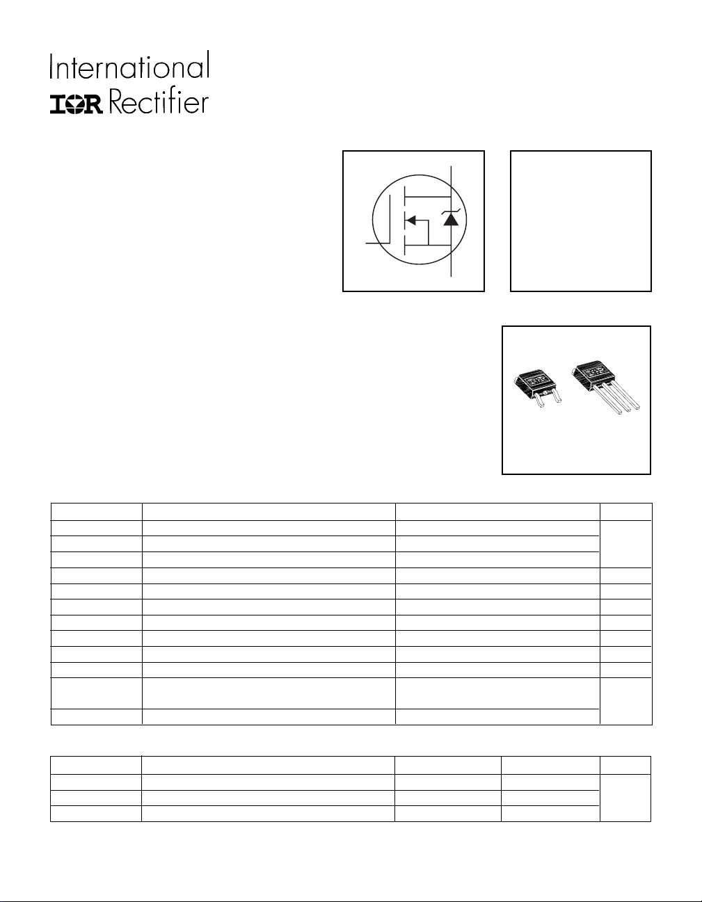
G
Description
Fifth Generation HEXFETs from International Rectifier utilize advanced
processing techniques to achieve the lowest possible on-resistance per
silicon area. This benefit, combined with the fast switching speed and
ruggedized device design that HEXFET Power MOSFETs are well known for,
provides the designer with an extremely efficient device for use in a wide
variety of applications.
The D-PAK is designed for surface mounting using vapor phase, infrared, or
wave soldering techniques. The straight lead version (IRFU series) is for
through-hole mounting applications. Power dissipation levels up to 1.5 watts
are possible in typical surface mount applications.
Absolute Maximum Ratings
Parameter Max. Units
ID @ TC = 25°C Continuous Drain Current, VGS @ 10V 17
ID @ TC = 100°C Continuous Drain Current, VGS @ 10V 12 A
I
DM
PD @TC = 25°C Power Dissipation 45 W
V
GS
E
AS
I
AR
E
AR
dv/dt Peak Diode Recovery dv/dt 5.0 V/ns
T
J
T
STG
Pulsed Drain Current 68
Linear Derating Factor 0.30 W/°C
Gate-to-Source Voltage ± 20 V
Single Pulse Avalanche Energy 71 mJ
Avalanche Current 10 A
Repetitive Avalanche Energy 4.5 mJ
Operating Junction and -55 to + 175
Storage Temperature Range
Soldering Temperature, for 10 seconds 300 (1.6mm from case )
D
V
= 55V
DSS
R
DS(on)
= 0.075Ω
ID = 17A
S
D - P ak
TO-252AA
I-P a k
TO-251AA
°C
Thermal Resistance
Parameter Typ. Max. Units
R
θJC
R
θJA
R
θJA
** When mounted on 1" square PCB (FR-4 or G-10 Material ) .
For recommended footprint and soldering techniques refer to application note #AN-994
Junction-to-Case ––– 3.3
Case-to-Ambient (PCB mount)** ––– 50 °C/W
Junction-to-Ambient ––– 110
www.irf.com 1
Page 2
IRFR/U024N
Electrical Characteristics @ TJ = 25°C (unless otherwise specified)
Parameter Min. Typ. Max. Units Conditions
V
(BR)DSS
∆V
(BR)DSS
R
DS(on)
V
GS(th)
g
fs
I
DSS
I
GSS
Q
g
Q
gs
Q
gd
t
d(on)
t
r
t
d(off)
t
f
L
D
L
S
C
iss
C
oss
C
rss
Drain-to-Source Breakdown Voltage 55 ––– ––– V VGS = 0V, ID = 250µA
/∆T
Breakdown Voltage Temp. Coefficient ––– 0.052 ––– V/°C Reference to 25°C, ID = 1mA
J
Static Drain-to-Source On-Resistance ––– ––– 0.075 Ω VGS = 10V, ID = 10A
Gate Threshold Voltage 2.0 ––– 4.0 V VDS = VGS, ID = 250µA
Forward Transconductance 4.5 ––– ––– S VDS = 25V, ID = 10A
Drain-to-Source Leakage Current
––– ––– 25
––– ––– 250 VDS = 44V, VGS = 0V, TJ = 150°C
Gate-to-Source Forward Leakage ––– ––– 100 VGS = 20V
Gate-to-Source Reverse Leakage ––– ––– -100
VDS = 55V, VGS = 0V
µA
nA
VGS = -20V
Total Gate Charge ––– ––– 20 ID = 10A
Gate-to-Source Charge ––– ––– 5.3 nC VDS = 44V
Gate-to-Drain ("Miller") Charge ––– ––– 7.6 VGS = 10V, See Fig. 6 and 13
Turn-On Delay Time ––– 4.9 ––– VDD = 28V
Rise Time ––– 34 ––– ID = 10A
Turn-Off Delay Time ––– 19 ––– RG = 24Ω
ns
Fall Time ––– 27 ––– RD = 2.6Ω, See Fig. 10
4.5
Internal Drain Inductance
Internal Source Inductance ––– –––
––– –––
7.5
Between lead,
6mm (0.25in.)
nH
from package
and center of die contact
Input Capacitance ––– 370 ––– VGS = 0V
Output Capacitance ––– 140 ––– pF VDS = 25V
Reverse Transfer Capacitance ––– 65 ––– ƒ = 1.0MHz, See Fig. 5
D
G
S
Source-Drain Ratings and Characteristics
Parameter Min. Typ. Max. Units Conditions
I
S
I
SM
V
SD
t
rr
Q
rr
t
on
Continuous Source Current MOSFET symbol
(Body Diode)
Pulsed Source Current integral reverse
(Body Diode)
––– –––
––– –––
17
68
showing the
A
p-n junction diode.
G
Diode Forward Voltage ––– ––– 1.3 V TJ = 25°C, IS = 10A, VGS = 0V
Reverse Recovery Time ––– 56 83 ns TJ = 25°C, IF = 10A
Reverse RecoveryCharge ––– 120 180 nC di/dt = 100A/µs
Forward Turn-On Time Intrinsic turn-on time is negligible (turn-on is dominated by LS+LD)
Notes:
Repetitive rating; pulse width limited by
Pulse width ≤ 300µs; duty cycle ≤ 2%.
max. junction temperature. ( See fig. 11 )
V
= 25V, starting TJ = 25°C, L = 1.0mH
DD
RG = 25Ω, I
I
≤ 10A, di/dt ≤ 280A/µs, V
SD
= 10A. (See Figure 12)
AS
DD
≤ V
(BR)DSS
This is applied for I-PAK, L
lead and center of die contact.
,
Uses IRFZ24N data and test conditions.
of D-PAK is measured between
S
TJ ≤ 175°C
2 www.irf.com
D
S
Page 3
IRFR/U024N
A
A
)
A
A
100
VGS
TOP 15V
10V
8.0V
7.0V
6.0V
5.5V
5.0V
BOT TOM 4. 5V
10
D
I , D ra in-to -S o u rc e C u rre n t (A )
4.5V
20µs PULS E WIDTH
T = 25°C
1
0.1 1 10 100
V , Dra in-t o -S o u rc e V o ltage (V)
DS
100
C
100
VGS
TOP 15V
10V
8.0V
7.0V
6.0V
5.5V
5.0V
BOTTOM 4.5V
10
4.5V
D
I , D ra in-to -S o u rc e C u rre n t (A )
20µs PULS E WIDTH
T = 175°C
1
0.1 1 10 100
V , Dra in-t o -S o u rc e V o ltage (V)
DS
C
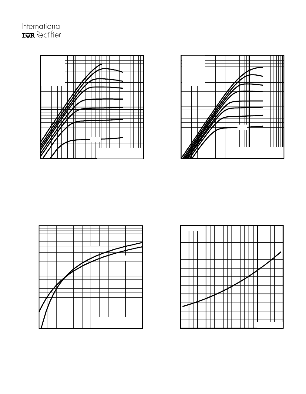
Fig 2. Typical Output CharacteristicsFig 1. Typical Output Characteristics
3.0
I = 1 7A
D
2.5
T = 25°C
J
T = 175°C
J
10
D
I , Drain-to-Source Current (A)
1
45678910
V , Ga te - to -S ou rc e V o ltage (V
GS
V = 25V
DS
20µs PULSE W IDTH
Fig 3. Typical Transfer Characteristics
2.0
1.5
(N o rma lize d )
1.0
0.5
DS(on)
R , D ra in -to -S o u rc e On R e s is tan c e
0.0
-60 -40 -20 0 20 40 60 80 100 120 140 160 180
T , Junction Tem pe rature (°C)
J
Fig 4. Normalized On-Resistance
V = 10 V
GS
Vs. Temperature
www.irf.com 3
Page 4

IRFR/U024N
A
g
g
g
A
)
A
A
700
600
500
400
300
C, Capacitance (pF)
200
100
0
1 10 100
V = 0V, f = 1M Hz
GS
C = C + C , C S H O RTE D
iss
C = C
C = C + C
C
iss
C
oss
C
rss
V , D rain-to-Source V oltage (V)
DS
s gd ds
rss
d
oss d s
d
Fig 5. Typical Capacitance Vs.
Drain-to-Source Voltage
100
20
I = 10 A
V , Ga te -to -S o ur ce Volta ge (V)
16
12
GS
D
8
4
V = 44 V
DS
V = 28 V
DS
FOR TEST CIRCUIT
0
048121620
Q , To ta l Ga te C h a rge (nC)
G
SEE FIGURE 13
Fig 6. Typical Gate Charge Vs.
Gate-to-Source Voltage
1000
O P E R A T IO N IN T H IS A R E A LIMITE D
BY R
DS(on)
T = 175°C
J
T = 25°C
J
10
SD
I , Reverse Drain Current (A)
1
0.4 0.6 0.8 1.0 1.2 1.4 1.6 1.8 2.0
V , So urce-to-Drain Voltage (V
SD
V = 0V
Fig 7. Typical Source-Drain Diode
GS
100
10
D
I , Drain Current (A)
T = 2 5 ° C
C
T = 175°C
J
Single Pulse
1
1 10 100
V , Dra in-t o -S o u rc e V o ltage (V)
DS
Fig 8. Maximum Safe Operating Area
10µs
100µs
1ms
10ms
Forward Voltage
4 www.irf.com
Page 5

IRFR/U024N
A
20
16
12
8
D
I , Drain Current (Am ps)
4
0
25 50 75 100 125 150 175
T , Cas e Temperature (°C)
C
Fig 9. Maximum Drain Current Vs.
Case Temperature
10
R
V
DS
V
GS
R
G
D
D.U.T.
4.5V
Pulse Width ≤ 1 µs
Duty Factor ≤ 0.1 %
Fig 10a. Switching Time Test Circuit
V
DS
90%
10%
V
GS
t
d(on)tr
t
d(off)tf
Fig 10b. Switching Time Waveforms
+
V
DD
-
D = 0.50
thJC
1
0.20
0.10
0.05
0.02
0.01
0.1
T h e rmal Re s p o n s e (Z )
0.01
0.00001 0.0001 0.001 0.01 0.1 1
SINGLE PULSE
(THERMAL RESPONSE)
Notes :
1. Duty factor D = t / t
2. Pea k T = P x Z + T
t , Re c ta ngular Pulse Duration (sec)
1
J
DM
P
DM
t
1
t
2
2
1
thJC
C
A
Fig 11. Maximum Effective Transient Thermal Impedance, Junction-to-Case
www.irf.com 5
Page 6

IRFR/U024N
A
A
15V
DRIVER
R
G
20V
V
DS
t
L
D.U.T
I
AS
0.01
p
Ω
Fig 12a. Unclamped Inductive Test
Circuit
V
(BR)DSS
t
p
140
120
100
80
+
V
DD
-
60
40
20
AS
V = 25 V
E , Single Pulse Avalanche Energy (mJ)
DD
0
25 50 75 100 125 150 175
Starting T , Junction Temperature (°C)
J
I
TO P 4.2A
7.2A
BOTTO M 10A
D
Fig 12c. Maximum Avalanche Energy
Vs. Drain Current
I
AS
Fig 12b. Unclamped Inductive Waveforms
Q
G
10 V
Q
GS
V
G
Q
GD
Charge
Fig 13a. Basic Gate Charge Waveform
Current Regulator
Same Type as D.U.T.
50KΩ
12V
.2µF
V
GS
.3µF
D.U.T.
3mA
I
G
Current Sampling Resistors
I
+
V
-
D
Fig 13b. Gate Charge Test Circuit
DS
6 www.irf.com
Page 7

IRFR/U024N
Peak Diode Recovery dv/dt Test Circuit
D.U.T
+
-
R
G
Driver Gate Drive
P.W.
+
Circuit Layout Considerations
• Low Stray Inductance
• Ground Plane
• Low Leakage Inductance
Current Transformer
-
-
• dv/dt controlled by R
G
• Driver same type as D.U.T.
• ISD controlled by Duty Factor "D"
• D.U.T. - Device Under Test
Period
D =
P.W.
Period
+
+
V
DD
-
VGS=10V
*
D.U.T. ISDWaveform
Reverse
Recovery
Current
Re-Applied
Voltage
D.U.T. VDSWaveform
Inductor Curent
* V
= 5V for Logic Level Devices
GS
Body Diode Forward
Current
di/dt
Diode Recovery
dv/dt
Body Diode Forward Drop
Ripple ≤ 5%
V
DD
I
SD
Fig 14. For N-Channel HEXFETS
www.irf.com 7
Page 8

IRFR/U024N
A
Package Outline
TO-252AA Outline
Dimensions are shown in millimeters (inches)
6.73 (.265)
6.35 (.250)
- A -
5.46 (.215)
5.21 (.205)
4
6.22 (.245)
1.02 (.040)
1.64 (.025)
1.52 (.060)
1.15 (.045)
1.14 (.045)
2X
0.76 (.030)
2.28 (.090)
1 2 3
5.97 (.235)
0.89 (.035)
3X
0.64 (.025)
0.25 (.010) M A M B
4.57 (.180)
Part Marking Information
TO-252AA (D-PARK)
- B -
1.27 (.050)
0.88 (.035)
2.38 (.094)
2.19 (.086)
10.42 (.410)
9.40 (.370)
NOTES:
1 DIMEN SIONING & TOLERANCING PER ANSI Y14.5M, 1982.
2 CONTROLLING DIMENSION : INCH.
3 CONFORMS TO JEDEC OUTLINE TO-252AA.
4 DIMENSIONS SHOWN ARE BEF ORE SOLDER DIP,
SOLDER DIP MAX. +0.16 (.006).
1.14 (.045)
0.89 (.035)
0.58 (.023)
0.46 (.018)
6.45 (.245)
5.68 (.224)
0.51 (.020)
MIN .
0.58 (.023)
0.46 (.018)
LEAD ASSIGNMENTS
1 - G A TE
2 - D RA IN
3 - S OURC E
4 - D RA IN
E X A MP L E : T HIS IS AN IRF R1 2 0
WITH ASSEMBLY
L OT C OD E 9U 1 P
INTERN ATIONA L
RECTIFIER
L OG O
IRFR
120
FIRST PO RTION
OF PART NUMBER
9 U 1 P
ASSEMBLY
L OT C OD E
SECOND PORTION
OF PART NUMBER
8 www.irf.com
Page 9

Package Outline
R
TO-251AA Outline
Dimensions are shown in millimeters (inches)
IRFR/U024N
6.73 (.265)
6.35 (.250)
5.46 (.215)
5.21 (.205)
1.52 (.060)
1.15 (.045)
- B -
2.28 (.090)
1.91 (.075)
1.14 (.045)
3X
0.76 (.030)
2.28 (.090)
- A -
4
1 2 3
3X
2X
1.27 (.050)
0.88 (.035)
6.22 (.245)
5.97 (.235)
9.65 (.380)
8.89 (.350)
0.89 (.035)
0.64 (.025)
0.25 (.0 1 0) M A M B
Part Marking Information
TO-251AA (I-PARK)
2.38 (.094)
2.19 (.086)
0.58 (.023)
0.46 (.018)
6.45 (.245)
5.68 (.224)
NOTES:
1 D IMENSION ING & T O LE R A NCING PE R A NSI Y14.5M, 1982.
2 CONTROLLING DIMENSION : INCH.
3 CONFORMS TO JEDEC OUTLINE TO-252AA.
4 DIMENSIONS SHOWN ARE BEFORE SOLDER DIP,
SO LDER DIP MAX. +0.16 (.006).
1.14 (.045)
0.89 (.035)
0.58 (.023)
0.46 (.018)
LEAD ASSIGNMENTS
1 - GA T E
2 - DR A IN
3 - SO URCE
4 - DR A IN
E X A MP L E : T HIS IS AN I R F U1 2 0
WITH ASSEMBLY
L OT CO DE 9 U 1 P
INTE RNATIONAL
R E CT IF IER
L OG O
IR F U
120
F IR S T P O RT IO N
OF PART NUMBE
9U 1P
ASSEMBLY
L O T C OD E
SECOND PORTION
OF PART NUMBER
www.irf.com 9
Page 10

IRFR/U024N
Tape & Reel Information
TO-252AA
Dimensions are shown in millimeters (inches)
TR
16 . 3 ( .641 )
15 . 7 ( .619 )
12 .1 ( .4 7 6 )
11 .9 ( .4 6 9 )
NOTES :
1. CONTROLLING DIMENSION : MILLIMETER.
2. ALL DIMENSIONS ARE SHOWN IN MILLIMETERS ( INCHES ).
3. OU TLINE CONFORM S TO EIA-481 & EIA-541.
13 INCH
FEED DIRECTION
8.1 ( .318 )
7.9 ( .312 )
TRR
TRL
16 .3 ( .6 4 1 )
15 .7 ( .6 1 9 )
FEED DIRECTION
16 m m
NOTES :
1. OUTLINE CONFO RM S TO EIA-481.
WORLD HEADQUARTERS: 233 Kansas St., El Segundo, California 90245, Tel: (310) 322 3331
EUROPEAN HEADQUARTERS: Hurst Green, Oxted, Surrey RH8 9BB, UK Tel: ++ 44 1883 732020
IR CANADA: 7321 Victoria Park Ave., Suite 201, Markham, Ontario L3R 2Z8, Tel: (905) 475 1897
IR FAR EAST: K&H Bldg., 2F, 30-4 Nishi-Ikebukuro 3-Chome, Toshima-Ku, Tokyo Japan 171 Tel: 81 3 3983 0086
IR SOUTHEAST ASIA: 315 Outram Road, #10-02 Tan Boon Liat Building, Singapore 0316 Tel: 65 221 8371
IR GERMANY: Saalburgstrasse 157, 61350 Bad Homburg Tel: ++ 49 6172 96590
IR ITALY: Via Liguria 49, 10071 Borgaro, Torino Tel: ++ 39 11 451 0111
http://www.irf.com/ Data and specifications subject to change without notice. 4/98
10 www.irf.com
 Loading...