

Page 1
PD- 93844B
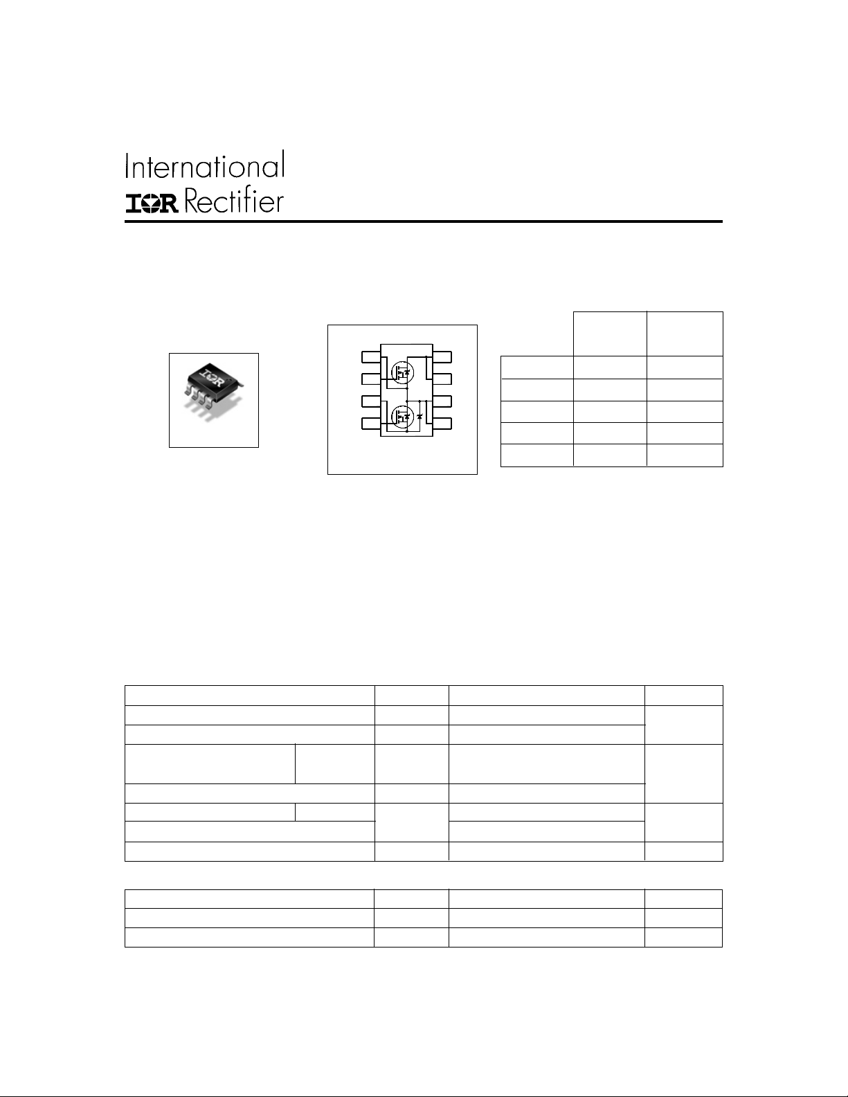
IRF7901D1
• Co-Pack Dual N-channel HEXFET Power MOSFET
and Schottky Diode
• Ideal for Synchronous Buck DC-DC
Converters Up to 5A Peak Output
• Low Conduction Losses
• Low Switching Losses
• Low Vf Schottky Rectifier
Q1
18
Source
Q1
27
Gate
PGND
3
Q2
4
SO-8
Gate
Co-Packaged Dual MOSFET Plus Schottky Diode
Device Ratings (Max.V alues)
Q1 Q2
Pwr
Top View
Vin
Pwr
Vin
Pwr
6
Vout
Pwr
5
Vout
V
DS
R
(on)
DS
Q
G
Q
sw
V
SD
Dual FETKY™
and Schottky
30V 30V
38 mΩ 32 mΩ
10.5 nC 18.3 nC
3.8 nC 9.0 nC
1.0V 0.52V
Description
™
The FETKY
family of Co-Pack HEXFETMOSFETs and Schottky diodes offers the designer an innovative,
board space saving solution for switching regulator and power management applications. Advanced
HEXFETMOSFETs combined with low forward drop Schottky results in an e xtremely efficient de vice suitable
for a wide variety of portable electronics applications.
The SO-8 has been modified through a customized leadframe for enhanced thermal characteristics and multiple
die capability making it ideal in a variety of power applications. With these improvements, multiple devices can
be used in an application with dramatically reduced board space. Internal connections enable easier board
layout design with reduced stray inductance.
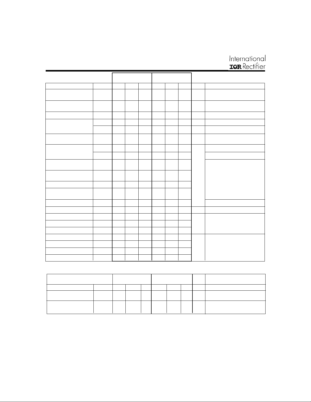
Absolute Maximum Ratings
Parameter Symbol IRF7901D1 Units
Drain-Source Voltage V
Gate-Source Voltage V
Continuous Output TL = 100°C I
DS
GS
6.2 A
D
30 V
±20
Current (VGS ≥ 4.5V)
Pulsed Drain Current I
Power Dissipation TL = 100°C P
Junction & Storage Temperature Range TJ, T
Pulsed Source Current I
24
DM
D
STG
12 A
SM
2.0 W
–55 to 150 °C
Thermal Resistance
Parameter Max. Units
Maximum Junction-to-Ambient R
Maximum Junction-to-Lead R
θJA
θJL
62.5 °C/W
25 °C/W
www.irf.com 1
9/19/01
Page 2
IRF7901D1
Electrical Characteristics
Q1 - Control FET Q2 - Synch FET
& Schottky
Parameter Min Typ Ma x Min Typ M ax Units Conditions
Drain-to-Source BV
Breakdown V oltage*
Static Drain-Source R
on Resistance*
Gate Threshold V oltage* V
Drain-Source Leakage I
Gate-Source Leakage I
Current*
DSS
GSS
T otal Gate Charge* Q
Q
Pre-Vth Q
Gate-Source Charge
Post-Vth Q
Gate-Source Charge
Gate to Drain Charge Q
Switch Charge* Q
(Q
+ Qgd)
gs2
Output Charge* Q
Gate Resistance R
Input Capacitance C
Output Capacitance C
T ransf er Capacitance C
T urn-On Delay Time t
Rise Time t
T urn-Off Delay Time t
Fall Time t
d
r
d
f
DS
GS
G cont
G synch
GS1
GS2
GD
sw
oss
G
iss
oss
rss
(on) – 7.2 – – 10.4 – VDD = 16V , ID = 5A, VGS = 5V
(off) – 14.7 – – 14.6 – See test diagram Fig 17.
30 – – 30 – – V VGS = 0V , ID = 250µA
DSS
(on) – 28 38 – 23 3 2 mΩ VGS = 4.5V , ID = 5A
(th) 1.0 – – 1.0 – – V VDS = VGS, ID = 250µA
– – 30 – – 30 µA VDS = 24V , VGS = 0
– – 0.15 – – 4.3 m A V
= 24V , V
DS
= 0, TJ = 125°C
GS
– – ±100 – – ±100 nA VGS = ±20V
– 7.6 10.5 – 15.5 21.0 VGS = 5V , VDS = 16V , ID = 5A
–6.79.0–13.518.3V
= 5V , VDS= 100mV , ID = 5A
GS
– 2.0 – – 5.5 – VDS = 16V , ID = 5A
– 0.5 – – 0.9 – nC
– 1.9 – – 4.7 –
–2.43.8–5.69.0
– 13.5 18.0 – 9.0 12.3 VDS = 16V , VGS = 0
– 3.4 – – 4.3 – Ω
– 780 – – 1810 –
– 430 – – 310 – pF VDS = 16V , VGS = 0, f = 1MHz
– 30 – – 110 –
– 13.8 – – 16.4 – ns Clamped inductive load
–8––5.2–
Source-Drain Ratings and Characteristics
Q1 Q2 &
parallel Schottky
Parameter Min Typ Max Min Typ Max Units Conditions
Diode Forward V
k
V oltage*
SD
Reverse Recovery Q
Charge V
Repetitive rating; pulse width limited by max. junction temperature.
Pulse width ≤ 300 µs; duty cycle ≤ 2%.
When mounted on 1 inch square copper board, t < 10 sec.
– 0.7 1.0 – 0.48 0.52 V IS = 1A, VGS = 0V
– 62.3 – – 8.9 – nC dl/dt = 700A/us
rr
m Combined Q1, Q2 I
current based on maximum allowable junction temperature;
switching or other losses will decrease RMS current capability
When mounted on IRNBPS2 design kit. Measured as device T
to Pwr leads (Vin & V
* Devices are 100% tested to these parameters.
@ Pwr V
RMS
)
out
= 16V , VGS = 0V , IS = 5A
DS
pins. Calculated continuous
out
www.irf.com2
J
Page 3
IRF7901D1
Power MOSFET Optimization f or DC-DC Converters
Table 1 and Table 2 describes the event during the various charge segments and shows an approximation of losses during
that period.
Conduction
Loss
Gate Drive
Loss
Switching
Loss
Losses associated with MOSFET on time. I
current and duty cycle.
Losses associated with charging and discharging the gate of the
MOSFET every cycle. Use the control FET QG.
Losses during the drain voltage and drain current transitions for every full
cycle.
Losses occur during the Q
Output
Loss
using Q
Losses associated with the Q
FET turns on. Losses are caused by both FETs, but are dissipated by the
switch
.
control FET .
Conduction
Loss
Gate Drive
Loss
Switching
Loss
Losses associated with MOSFET on time. I
duty cycle.
Losses associated with charging and discharging the gate of the MOSFET
every cycle. Use the Sync FET QG.
Generally small enough to ignore except at light loads when the current
reverses in the output inductor. Under these conditions various light load
power saving techniques are employed by the control IC to maintain switching
losses to a negligible level.
Output
Loss
Losses associated with the Q
turns on. They are caused by the synchronous FET, but are dissipated in the
control FET .
Typical Application
The performance of the new Dual FETKY
Synchronous Buck Design Kit”, operating up to 21V
1V
out
to 5V
out
.
Table 1 – Control FET Losses
Segment LossesDescription
is a function of load
RMS
2
and QGD time period and can be simplified by
GS2
of the device every cycle when the control
OSS
P
OUTPUT
Table 2 – Synchronous FET Losses
Segment LossesDescription
is a function of load current and
RMS
≈
SWITCH
P
OUTPUT
of the device every cycle when the control FET
OSS
TM
has been tested in-circuit using IR’s new IRNBPS2 “Dual Output
and 5A peak output current, with operating voltages from
in
2
×=
RIP
ƒ××=
QVP
GGIN
Q
GS
IVP
LINQGS
I
G
Q
GD
IVP
LINQGD
I
G
Q
SW
IVP
LINSWITCH
I
OSS
2
2
GGIN
G
V
IN
×=
RIP
DSonRMSCOND
ƒ××=
Q
QVP
0P
Q
OSS
V
IN
2
)on(DSRMSCOND
2
ƒ×××≈
ƒ×××≈
ƒ××≈
ƒ××=
ƒ××=
Q2
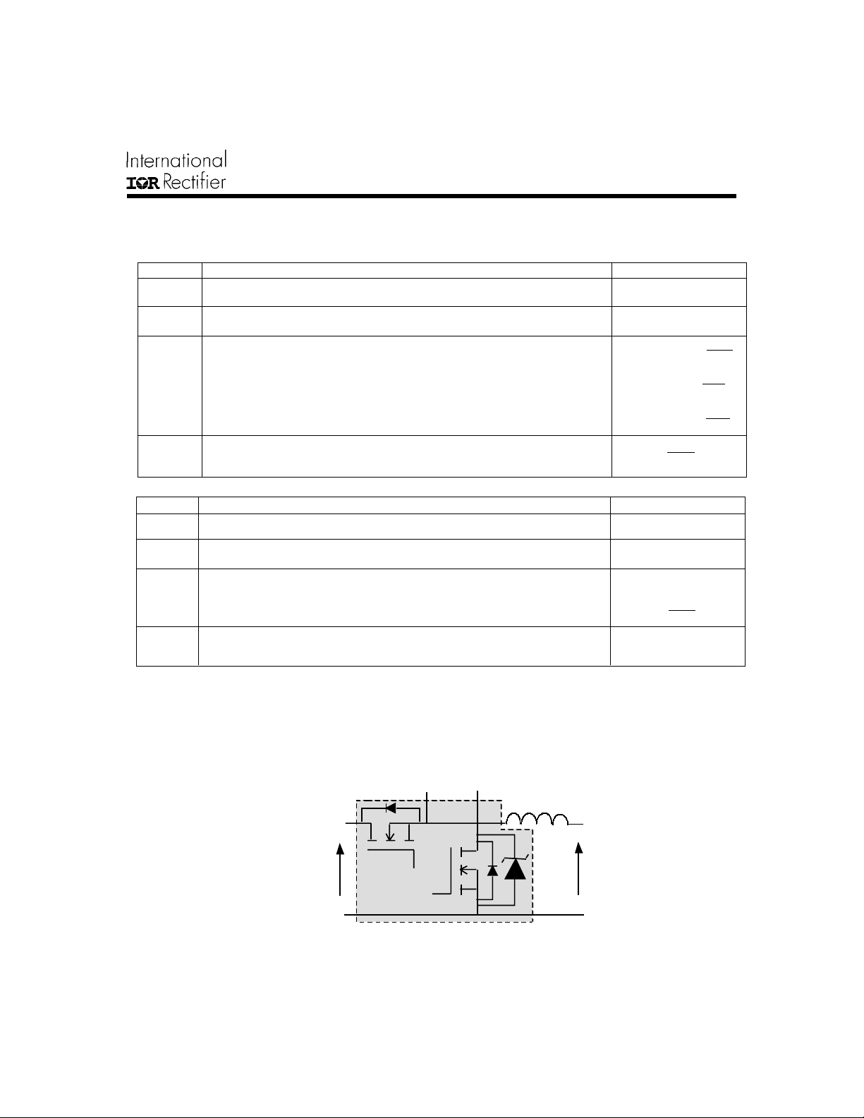
Pin 5&6
Pwr Vout
Sha ded area = Du al FETKY
Schottky
Vout
Pin 7&8
Pwr Vin
Vin
Pin 3
PGND
Q1
Pin 2
Q1 Gate
Pin 1
Q1 Sourc e
Pin 4
Q2 Gate
Figure 1: Synchronous Buck dc-dc
T opology
www.irf.com 3
Page 4

IRF7901D1
Typical Application (Contd.)
The Dual FETKY integrates all the power semiconductor devices for DC-DC conversion within one SO-8
package, as shown on page 1. The high side control MOSFET (Q1) is optimized for low combined Qsw and
(on). The low side synchronous MOSFET (Q2) is optimized for low RDS(on) and high Cdv/dt immunity. The
R
DS
ultra-low V
deadtime efficiency. For ease of circuit board layout, the Dual FETKY has been internally configured such that
it represents a functional block for the power device portion of the synchronous buck DC-DC converter. This
helps to minimize the external PCB traces compared to a discrete solution.
In-Circuit Efficiency
The in-circuit efficiency curves for the Dual FETKY are shown in Figure 2 & 3. The Dual FETKY can
achieve up to 96.6% and 94.6% peak efficiency for the 5.0V and 3.3V applications respectively, with
excellent maximum load efficiency.
DC-DC for 3.3V
97%
95%
93%
Efficiency (%)
91%
89%
Figure 2. IRF7901D1 Dual FETKYTM electrical efficiency
schottky diode is internally connected in parallel with the synchronous MOSFET, for improved
f
IRF7901D1 Dual FETKYTM performance i n S ynchronous Buck
1 1.5 2 2.5 3 3.5 4 4.5 5
out
& 5.0V
@ 300kHz, using IRNBPS2 design kit
out
10.8Vin / 3.3Vout
14Vin / 3.3Vout
21Vin / 3.3Vout
10.8Vin / 5.0Vout
14Vin / 5.0Vout
21Vin / 5.0Vout
Output Current (A)
IRF7901D1 Dual FETKYTM performance in Synchronous Buck
DC-DC for 1 .0V
90%
88%
86%
84%
82%
80%
78%
Efficiency (%)
76%
74%
72%
70%
1.5 2 2.5 3 3.5 4 4.5 5
@ 300kHz, using IRNBPS2 design kit
out
8.4Vin / 1.0Vout
14Vin / 1.0Vout
Output Current (A)
Figure 3. IRF7901D1 Dual FETKYTM electrical efficiency
at 3.3Vout & 5.0Vout.
at 1.0Vout.
Q1 - Control FET Q2 - Synchronous FET & Schottky
Typical Characteristics
2.0
ID = 5.0A
V
= 4.5V
GS
1.5
1.0
, Drain-to-Source On Resistance
DS(on)
(Normalized)
R
0.5
-60 -40 -20 0 20 40 60 80 100 120 140 160
TJ , Junction Temperature (°C)
Figure 4. Normalized On-Resistance vs Junction
Temperature
1.50
ID = 5.0A
V
= 4.5V
GS
1.25
1.00
, Drain-to-Source On Resistance
DS(on)
(Normalized)
R
0.75
-60 -40 -20 0 20 40 60 80 100 120 140 160
TJ , Junction Temperature (°C)
Figure 5. Normalized On-Resistance vs Junction
Temperature
www.irf.com4
Page 5

IRF7901D1
Q1 - Control FET Q2 - Synchronous FET & Schottky
Typical Characteristics
6.0
ID= 5.0A
V
= 16V
DS
4.0
2.0
, Gate-to-Source Voltage (V)
GS
V
0.0
0.0 2.0 4.0 6.0 8.0
QG, Total Gate Charge (nC)
Figure 6. Gate-to-Source Voltage vs Typical Gate
)
0.05
Ω
0.04
0.03
, Drain-to -Source On Resistance (
Charge
ID = 5.0A
6.0
ID= 5.0A
V
= 16V
DS
4.0
2.0
, Gate-to-Source Voltage (V)
GS
V
0.0
0 4 8 12 16
QG, Total Gate Charge (nC)
Figure 7. Gate-to-Source Voltage vs Typical Gate
)
Ω
, Drain-to -Source On Resistance (
0.030
0.025
0.020
0.015
Charge
ID = 5.0A
DS(on)
0.02
R
3.0 4.0 5.0 6.0 7.0 8.0 9.0 10.0
V
Gate -to -Source Voltage (V)
GS,
Figure 8. Typical RDS(on) vs Gate-to-Source Voltage
30
20
VGS
TOP 10 V
8.0V
4.5V
3.5V
3.0V
2.5V
2.0V
BOTTOM 0.0V
DS(on)
0.010
R
4.0 5.0 6.0 7.0 8.0 9.0 10.0
V
Gate -to -Source Voltage (V)
GS,
Figure 9. Typical RDS(on) vs Gate-to-Source Voltage
50
40
30
20
VGS
TOP 10V
8.0V
4.5V
3.5V
3.0V
2.5V
2.0V
BOTTOM 0.0V
10
, Drai n -to-Source Curren t (A)
D
I
0
0.0V
250µs PULSE WIDTH
Tj = 25°C
0.0 0.4 0.8 1.2 1.6 2.0
VSD, Source-To-Drain Voltage (V)
V
, Drain-toSource Voltage (V)
DS
, Drain-to-Source Current (A)
10
D
I
0
0.0 0.4 0.8 1.2
VSD, Source-To-Drain Voltage (V)
V
, Drain-toSource Volt age (V)
DS
0.0V
250µs PULSE WIDTH
Tj = 25°C
Figure 10. Typical Reverse Output Characteristics Figure 11. Typical Reverse Output Characteristics
www.irf.com 5
Page 6

IRF7901D1
Q1 - Control FET Q2 - Synchronous FET & Schottky
Typical Characteristics
, Drain-to-Source Current (A)
I
100.00
)
(Α
10.00
, Drain-to-Source Current
D
I
50
40
30
20
10
D
0
1.00
0.10
VGS
TOP 10V
8 .0 V
4 .5 V
3 .5 V
3 .0 V
2 .5 V
2 .0 V
BOTTOM 0.0V
0.0V
250µs PULSE WIDTH
Tj = 150°C
0.0 0.4 0.8 1.2
VSD, Source-To-Drain Voltage (V)
V
, Drain-toSource Voltage (V)
DS
TJ = 150°C
TJ = 25°C
V
= 10V
DS
250µs PULSE WIDTH
2.5 3. 0 3.5 4.0 4.5
VGS, Gate-to-Source Voltage (V)
30
20
10
, Drai n -to-Source Curren t (A)
D
I
0
VGS
TOP 10 V
8.0V
4.5V
3.5V
3.0V
2.5V
2.0V
BOTTOM 0.0V
0.0V
250µs PULSE WIDTH
Tj = 150°C
0.0 0.4 0.8 1.2 1.6 2.0
VSD, Source-To-Drain Voltage (V)
V
, Drain-toSource Voltage (V)
DS
Figure 12. Typical Reverse Output Characteristics Figure 13. Typical Reverse Output Characteristics
100.00
)
(Α
, Drain-to-Source Current
D
I
TJ = 150°C
10.00
1.00
TJ = 25°C
V
= 10V
DS
0.10
2.0 2.5 3.0 3.5 4.0 4.5
VGS, Gate-to-Source Voltage (V)
250µs PULSE WIDTH
Figure 14. Typical Transfer Characteristic Figure 15. Typical Transfer Characteristic
100
D = 0.50
thJA
0.20
10
0.10
0.05
0.02
1
0.01
Thermal Response (Z )
SINGLE PULSE
(THERMAL RE S PO NSE )
0.1
0.00001 0.0001 0.001 0.01 0.1 1 10 100
t , Rectangular P ulse Duration (sec)
1
Notes:
1. Du ty factor D = t / t
2. Peak T =P x Z + T
J DM thJA A
P
DM
t
1
t
2
1 2
Figure 16. Maximum Effective Transient Thermal Impedance, Junction-to-Ambient
www.irf.com6
Page 7

IRF7901D1
SO-8
Package
Outline
Part Marking
Information
Figure 17. Clamped Inductive Load Test Diagram and
Switching waveform.
www.irf.com 7
Page 8

IRF7901D1
SO-8 Tape & Reel Information
Dimensions are shown in millimeters (inches)
TERMINAL NUMBER 1
12.3 ( .48 4 )
11.7 ( .46 1 )
8.1 ( .318 )
7.9 ( .312 )
330.00
(12.992)
MAX.
NOTES :
1. CONTROLLING DIMENSION : MILLIMETER.
2. OUTLINE CONFORMS TO EIA-481 & EIA-541.
This product has been designed and qualified for the consumer market.
FEED DIRECTION
14.40 ( .566 )
12.40 ( .488 )
Data and specifications subject to change without notice.
Qualification Standards can be found on IR’s Web site.
IR WORLD HEADQUARTERS: 233 Kansas St., El Segundo, California 90245, USA Tel: (310) 252-7105
TAC Fax: (310) 252-7903
Visit us at www.irf.com for sales contact informatin.9/01
www.irf.com8
 Loading...