

Page 1
Octal D Flip-Flop with
Common Clock and Reset
High-Performance Silicon-Gate CMOS
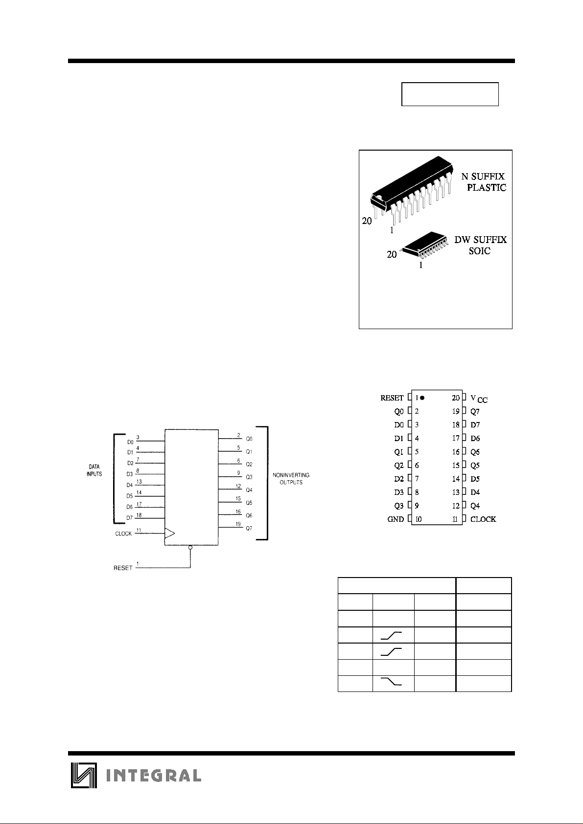
The IN74HC273A is identical in pinout to the LS/ALS273. The
device inputs are compatible with standard CMOS outputs; with pullup
resistors, they are compatible with LS/ALSTTL outputs.
This device consists of eight D flip-flops with common Clock and
Reset inputs. Each flip-flop is loaded with a low-to-high transition of
the Clock input. Reset is asynchronous and active low.
•
Outputs Directly Interface to CMOS, NMOS, and TTL
•
Operating Voltage Range: 2.0 to 6.0 V
•
Low Input Current: 1.0 µA
•
High Noise Immunity Characteristic of CMOS Devices
TECHNICAL DATA
IN74HC273A
ORDERING INFORMATION
IN74HC273AN Plastic
IN74HC273ADW SOIC
TA = -55° to 125° C for all packages
LOGIC DIAGRAM
PIN 20=V
PIN 10 = GND
CC
PIN ASSIGNMENT
FUNCTION TABLE
Inputs Output
Reset Clock D Q
LX X L
HHH
HLL
H L X no change
H X no change
X = don’t care
331
Page 2
IN74HC273A
MAXIMUM RATINGS
*
Symbol Parameter Value Unit
V
CC
V
V
OUT
I
IN
I
OUT
I
CC
P
DC Supply Voltage (Referenced to GND) -0.5 to +7.0 V
DC Input Voltage (Referenced to GND) -1.5 to VCC +1.5 V
IN
DC Output Voltage (Referenced to GND) -0.5 to VCC +0.5 V
DC Input Current, per Pin
DC Output Current, per Pin
DC Supply Current, VCC and GND Pins
Power Dissipation in Still Air, Plastic DIP+
D
SOIC Package+
±
20
±
35
±
75
750
500
Tstg Storage Temperature -65 to +150
T
Lead Temperature, 1 mm from Case for 10 Seconds
L
260
(Plastic DIP or SOIC Package)
*
Maximum Ratings are those values beyond which damage to the device may occur.
Functional operation should be restricted to the Recommended Operating Conditions.
+Derating - Plastic DIP: - 10 mW/°C from 65° to 125°C
SOIC Package: : - 7 mW/°C from 65° to 125°C
mA
mA
mA
mW
°
C
°
C
RECOMMENDED OPERATING CONDITIONS
Symbol Parameter Min Max Unit
V
CC
VIN, V
T
A
tr, t
f
This device c ontains p rote ction ci rcuitr y to guard a gainst damage d ue to high st atic voltages or electr ic
fields. However, precautions must be taken to avoid applications of any voltage higher than maximum rated
voltages to this high-impedance circuit. For proper operation, V
GND≤(V
Unused inputs must always be tied to an appropriate logic voltage level (e.g., either GND or V
Unused outputs must be left open.
DC Supply Voltage (Referenced to GND) 2.0 6.0 V
DC Input Voltage, Output Voltage (Referenced to GND) 0 V
OUT
Operating Temperature, All Package Types -55 +125
Input Rise and Fall Time (Figure 1) VCC =2.0 V
IN
or V
OUT
)≤VCC.
V
V
IN
=4.5 V
CC
=6.0 V
CC
and V
should be constrained to the range
OUT
0
0
0
CC
1000
500
400
V
°
C
ns
CC
).
332
Page 3

IN74HC273A
DC ELECTRICAL CHARACTERISTICS
(Voltages Referenced to GND)
Symbol Parameter Test Conditions V
V
V
V
OH
V
OL
I
IN
Minimum High-Level
IH
Input Voltage
Maximum Low -
IL
Level Input Voltage
Minimum High-Level
Output Voltage
Maximum Low-Level
Output Voltage
Maximum Input
V
=0.1 V or VCC-0.1 V
OUT
≤
I
20 µA
OUT
V
=0.1 V or VCC-0.1 V
OUT
≤
I
20 µA
OUT
VIN=VIH or V
≤
I
OUT
VIN=VIH or V
≤
I
OUT
≤
I
OUT
VIN= VIL or V
≤
I
OUT
VIN= VIL or V
≤
I
OUT
≤
I
OUT
IL
20 µA
IL
4.0 mA
5.2 mA
IH
20 µA
IH
4.0 mA
5.2 mA
VIN=VCC or GND 6.0
Leakage Current
I
CC
Maximum Quiescent
Supply Current
VIN=VCC or GND
=0µA
I
OUT
(per Package)
V
2.0
4.5
6.0
2.0
4.5
6.0
2.0
4.5
6.0
4.5
6.0
2.0
4.5
6.0
4.5
6.0
CC
Guaranteed Limit
25 °C
to
≤
85
°
C
-55°C
1.5
3.15
4.2
0.5
1.35
1.8
1.9
4.4
5.9
3.98
5.48
0.1
0.1
0.1
0.26
0.26
±
0.1
1.5
3.15
4.2
0.5
1.35
1.8
1.9
4.4
5.9
3.84
5.34
0.1
0.1
0.1
0.33
0.33
±
1.0±1.0
≤
12
°
1.5
3.15
4.2
0.5
1.35
1.8
1.9
4.4
5.9
3.7
5.2
0.1
0.1
0.1
0.4
0.4
6.0 4.0 40 160
Unit
5
C
V
V
V
V
µ
A
µ
A
333
Page 4

IN74HC273A
AC ELECTRICAL CHARACTERISTICS
(CL=50pF,Input tr=tf=6.0 ns)
Symbol Parameter V
f
max
Maximum Clock Frequency (50 % Duty Cycle)
(Figures 1 and 4)
t
PLH
, t
Maximum Propagati on Delay, Clock to Q
PHL
(Figures 1 and 4)
t
PHL
Maximum Propagation Delay , Reset to Q
(Figures 2 and 4)
t
TLH
, t
Maximum Output Transition Time, Any Output
THL
(Figures 1 and 4)
C
IN
Maximum Input Capacitance - 10 10 10 pF
Power Dissipation Capacitance (Per Enabled
Output)
C
PD
Used to determine the no-load dynamic power
consumption: P
D=CPDVCC
2
f+ICCV
CC
V
CC
25 °C
to
-55°C
2.0
4.5
6.0
2.0
4.5
6.0
2.0
4.5
6.0
2.0
4.5
6.0
6.0
30
35
145
29
25
145
29
25
75
15
13
Typical @25°C,V
Guaranteed Limit
≤85°
C≤125°C
5.0
24
28
180
36
31
180
36
31
95
19
16
CC
4.0
20
24
220
44
38
220
44
38
110
22
19
=5.0 V
48 pF
Unit
MHz
ns
ns
ns
TIMING REQUIREMENTS
(CL=50pF,Input tr=tf=6.0 ns)
Symbol Parameter V
t
SU
Minimum Set up T ime, Data to
Clock (Figure 3)
t
h
Minimum Hold Time, Clock
to Data (Figure 3)
t
rec
Minimum Rec overy Time,
Reset Inactive to Clock
(Figure 2)
t
w
Minimum Pulse Width , Clock
(Figure 1)
t
w
Minimum Pulse Width , Res et
(Figure 2)
t
r, tf
Maximum Input Rise an d Fall
Times (Figure 1)
V
2.0
4.5
6.0
2.0
4.5
6.0
2.0
4.5
6.0
2.0
4.5
6.0
2.0
4.5
6.0
2.0
4.5
6.0
CC
Guaranteed Limit
25 °C to-55°C
60
12
10
3.0
3.0
3.0
5.0
5.0
5.0
60
12
10
60
12
10
1000
500
400
≤85°
75
15
13
3.0
3.0
3.0
5.0
5.0
5.0
75
15
13
75
15
13
1000
500
400
C
≤
125°C
90
Unit
ns
18
15
3.0
ns
3.0
3.0
5.0
ns
5.0
5.0
90
ns
18
15
90
ns
18
15
1000
ns
500
400
334
Page 5

IN74HC273A
Figure 1. Switching Waveforms Figure 2. Switching Waveforms
Figure 3. Switching Waveforms Figure 4. Test Circuit
EXPANDED LOGIC DIAGRAM
335
 Loading...