

Page 1

TECHNICAL DATA
326
Quad 2-Input Data Selectors/Multiplexer
with 3-State Outputs
High-Performance Silicon-Gate CMOS
The IN74HC258 is identical in pinout to the LS/ALS258. The
device inputs are compatible with standard CMOS outputs; with pullup
resistors, they are compatible with LS/ALSTTL outputs.
This device selects a (4-bit) nibble from either the A or B inputs as
determined by the Select input. The nibble is presented at the outputs
in inverted form when the Output Enable pin is at a low level. A high
level on the Output Enable pin switches the outputs into the highimpedance state.
•
Outputs Directly Interface to CMOS, NMOS, and TTL
•
Operating Voltage Range: 2.0 to 6.0 V
•
Low Input Current: 1.0 µA
•
High Noise Immunity Characteristic of CMOS Devices
IN74HC258
ORDERING INFORMATION
IN74HC258N Plastic
IN74HC258D SOIC
TA = -55° to 125° C for all packages
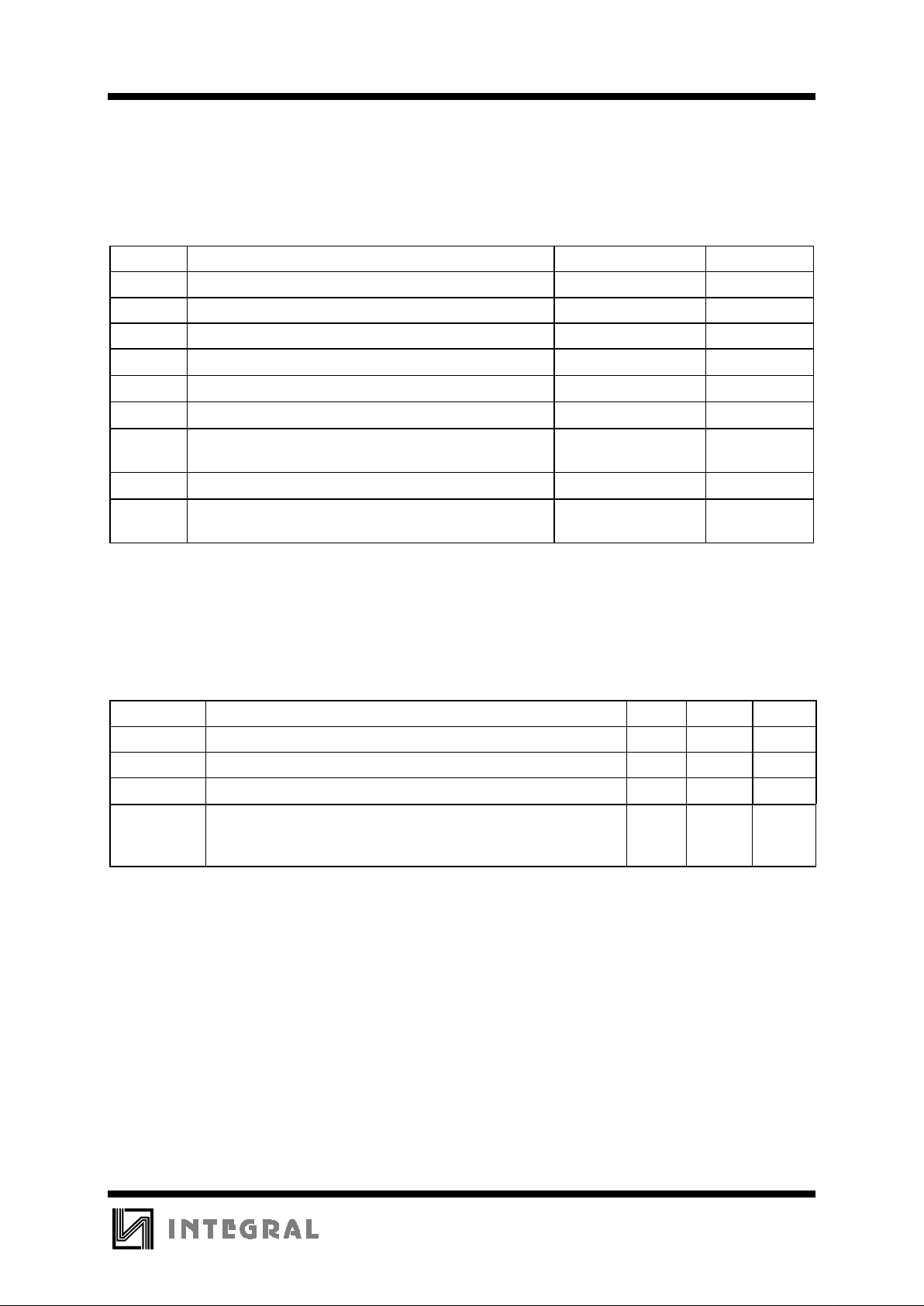
FUNCTION TABLE
Inputs Outputs
Output
Enable
Select Y0-Y3
HXZ
LLA0-A3
LHB0-B3
X=don’t care
Z = high-impedance st ate
A0-A3,B0-B3=the levels of the respective
Nibble Inputs
LOGIC DIAGRAM
PIN 16 =V
CC
PIN 8 = GND
PIN ASSIGNMENT
Page 2
IN74HC258
327
MAXIMUM RATINGS
*
Symbol Parameter Value Unit
V
CC
DC Supply Voltage (Referenced to GND) -0.5 to +7.0 V
V
IN
DC Input Voltage (Referenced to GND) -1.5 to VCC +1.5 V
V
OUT
DC Output Voltage (Referenced to GND) -0.5 to VCC +0.5 V
I
IN
DC Input Current, per Pin
±
20
mA
I
OUT
DC Output Current, per Pin
±
35
mA
I
CC
DC Supply Current, VCC and GND Pins
±
75
mA
P
D
Power Dissipation in Still Air, Plastic DIP+
SOIC Package+
750
500
mW
Tstg Storage Temperature -65 to +150
°
C
T
L
Lead Temperature, 1 mm from Case for 10 Seconds
(Plastic DIP or SOIC Package)
260
°
C
*
Maximum Ratings are those values beyond which damage to the device may occur.
Functional operation should be restricted to the Recommended Operating Conditions.
+Derating - Plastic DIP: - 10 mW/°C from 65° to 125°C
SOIC Package: : - 7 mW/°C from 65° to 125°C
RECOMMENDED OPERATING CONDITIONS
Symbol Parameter Min Max Unit
V
CC
DC Supply Voltage (Referenced to GND) 2.0 6.0 V
VIN, V
OUT
DC Input Voltage, Output Voltage (Referenced to GND) 0 V
CC
V
T
A
Operating Temperature, All Package Types -55 +125
°
C
tr, t
f
Input Rise and Fall Time (Figure 1) VCC =2.0 V
V
CC
=4.5 V
V
CC
=6.0 V
0
0
0
1000
500
400
ns
This device c ontains p rote ction ci rcuitr y to guard a gainst damage d ue to high st atic voltages or electr ic
fields. However, precautions must be taken to avoid applications of any voltage higher than maximum rated
voltages to this high-impedance circuit. For proper operation, V
IN
and V
OUT
should be constrained to the range
GND≤(V
IN
or V
OUT
)≤VCC.
Unused inputs must always be tied to an appropriate logic voltage level (e.g., either GND or V
CC
).
Unused outputs must be left open.
Page 3

IN74HC258
328
DC ELECTRICAL CHARACTERISTICS
(Voltages Referenced to GND)
V
CC
Guaranteed Limit
Symbol Parameter Test Conditions V
25 °C
to
-55°C
≤
85
°
C
≤
125
°
C
Unit
V
IH
Minimum High-Level
Input Voltage
V
OUT
=0.1 V or VCC-0.1 V
I
OUT
≤
20 µA
2.0
4.5
6.0
1.5
3.15
4.2
1.5
3.15
4.2
1.5
3.15
4.2
V
V
IL
Maximum Low Level Input Voltage
V
OUT
=0.1 V or VCC-0.1 V
I
OUT
≤
20 µA
2.0
4.5
6.0
0.3
0.9
1.2
0.3
0.9
1.2
0.3
0.9
1.2
V
V
OH
Minimum High-Level
Output Voltage
VIN=VIH or V
IL
I
OUT
≤
20 µA
2.0
4.5
6.0
1.9
4.4
5.9
1.9
4.4
5.9
1.9
4.4
5.9
V
VIN=VIH or V
IL
I
OUT
≤
6.0 mA
I
OUT
≤
7.8 mA
4.5
6.0
3.98
5.48
3.84
5.34
3.7
5.2
V
OL
Maximum Low- Level
Output Voltage
VIN=VIH or V
IL
I
OUT
≤
20 µA
2.0
4.5
6.0
0.1
0.1
0.1
0.1
0.1
0.1
0.1
0.1
0.1
V
VIN=VIH or V
IL
I
OUT
≤
6.0 mA
I
OUT
≤
.7.8 mA
4.5
6.0
0.26
0.26
0.33
0.33
0.4
0.4
I
IN
Maximum Input
Leakage Current
VIN=VCC or GND 6.0
±
0.1
±
1.0
±
1.0
µ
A
I
OZ
Maximum ThreeState Leakage
Current
Output in High-Impedance
State
V
IN
= VIL or V
IH
V
OUT
= V
CC
or GND
6.0
±
0.5
±
5.0
±
10
µ
A
I
CC
Maximum Quiescent
Supply Current
(per Package)
VIN=VCC or GND
I
OUT
=0µA
6.0 8.0 80 160
µ
A
Page 4

IN74HC258
329
AC ELECTRICAL CHARACTERISTICS
(CL=50pF,Input tr=tf=6.0 ns)
V
CC
Guaranteed Limit
Symbol Parameter V
25 °C
to
-55°C
≤85°C≤
125°C
Unit
t
PLH
, t
PHL
Maximum Propagation Delay, Nibble A or B to
Output Y (Figures 1and 4)
2.0
4.5
6.0
100
20
17
125
25
21
150
30
26
ns
t
PLH
, t
PHL
Maximum Propagation Delay , Select to
Output Y (Figures 2 and 4)
2.0
4.5
6.0
160
32
18
200
40
35
240
48
42
ns
t
PLZ
, t
PHZ
Maximum Propagation Delay , Output Enable to
Output Y (Figures 3 and 5)
2.0
4.5
6.0
150
30
26
190
38
33
225
45
38
ns
t
PZL
, t
PZH
Maximum Propagation Delay , Output Enable to
Output Y (Figures 3 and 5)
2.0
4.5
6.0
110
22
20
140
28
25
165
34
30
ns
t
TLH
, t
THL
Maximum Output Transition Time, Any Output
(Figures 1 and 4)
2.0
4.5
6.0
60
12
10
75
15
13
90
18
15
ns
C
IN
Maximum Input Capacitance - 10 10 10 pF
C
OUT
Maximum Three-State Output Capacitance
(Output in High-Impedance State)
-151515pF
Power Dissipation Capacitance (Per Package)
Typical @25°C,V
CC
=5.0 V
C
PD
Used to determine the no-load dynamic power
consumption:
P
D=CPDVCC
2
f+ICCV
CC
59 pF
Figure 1. Switching Waveforms Figure 2. Switching Waveforms
Page 5

IN74HC258
330
Figure 3. Switching Waveforms
Figure 4. Test Circuit Figure 5. Test Circuit
EXPANDED LOGIC DIAGRAM
 Loading...