

Page 1
Also included is a watchdog timer to stop and restart a
microprocessor that is “hung-up”. Three watchdog timeout periods are selectable: 150ms, 610ms and 1,200ms. If the
ST input is not strobed LOW before the time-out period
expires, a reset is issued.
Devices are available in 8-pin DIP, 8-pin SO and compact
8-pin MicroSO packages.
©
1999 IMP, Inc. 408-432-9100/www.impweb.com 1
Key Features
◆
Pin compatible with the Dallas Semiconductor
DS1832
— Over 40% lower supply current
◆
3.3V supply monitor
◆
Push-pull output
◆
Selectable watchdog period
◆
Debounce manual push-button reset input
◆
Precision temperature-compensated voltage
reference and comparator
◆
Power-up, power-down and brownout detection
◆
250ms minimum reset time
◆
Active LOW and HIGH reset signal
◆
Selectable trip point tolerance: 10% or 20%
◆
Low-cost 8-pin DIP/SO and 8-pin MicroSO
packages
◆
Wide operating temperature –40°C to +85°C
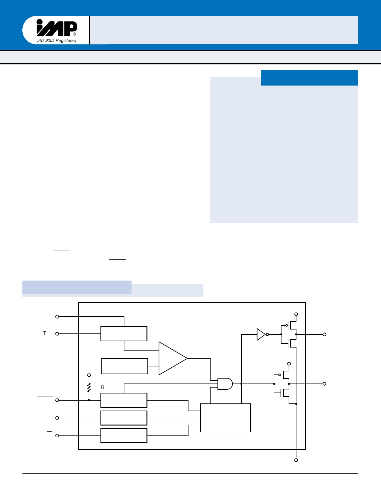
Block Diagram
IMP1
IMP1
832
832
POWER MANAGEMENT
3.3V
3.3V µµ
P P
P Pooww
er Suppl
er Supplyy
Monit
Monit
or and R
or and R
eset Cir
eset Cir
cuit
cuit
– Select
– Select
able T
able Trriipp-P-P
oint T
oint T
oler
oler
ance and
ance and
WWatc
atc
hdog P
hdog Perer
iod
iod
– Push-Butt
– Push-Butt
on R
on R
eset
eset
– Push-Pull R
– Push-Pull R
eset Outputs
eset Outputs
The IMP1832 microprocessor supervisor can halt and restart a “hungup” or “stalled” microprocessor, restart a microprocessor after a power
failure, and debounce a manual push-button microprocessor reset
switch. The IMP1832 features over 40% lower supply current than the
pin compatible Dallas Semiconductor DS1832.
Precision temperature compensated reference and comparator circuits
monitor the 3.3V, V
CC
input voltage. During power-up or when the V
CC
power supply falls outside selectable tolerance limits, both RESET and
RESET become active. When V
CC
rises above the threshold voltage, the
reset signals remain active for an additional 250ms minimum, allowing
the power supply and system microprocessor to stabilize. The trip point
tolerance signal, TOL, selects the trip level tolerance to be either 10- or
20-percent.
RESET and RESET outputs are push-pull.
A debounced manual reset input, PBRST, activates the reset outputs for
a minimum period of 250ms.
V
CC
TOL
PBRST
TD
ST
8
3
1
2
7
10%/20% Tolerance
V
CC
40k
W
Timebase Selection
Transition Detector
Selection
Reference
Push Button
Debounce
Watchdog
Watchdog
+
–
IMP1832
Reset &
Watchdog Timer
V
CC
6
V
CC
5
4
GND
RESET
RESET
1832_02.eps
Page 2
2
408-432-9100/www.impweb.com
©
1999 IMP, Inc.
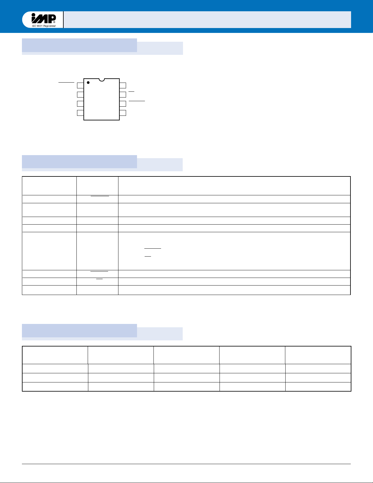
Pin Configuration
IMP1
IMP1
832
832
Pin Descriptions
Ordering Information
DIP/SO/MicroSO
rebmuNtraPegakcaP
erutarepmeTgnitarepO
egnaR
ylppuSmumixaM
(tnerruC µ )A
gnirotinoMegatloV
noitacilppA
2381PMIPID-8 – 04C° 58otC° 02V3.3
S2381PMIOS-8 – 04C° 58otC° 02V3.3
AMES2381PMIOSorciM-8 – 04C° 58otC° 02V3.3
spe.10t_2381
Pin Number
8-Pin Package Name Function
1 PBRST Debounced manual pushbutton reset input
2 TD Watchdog time delay selection. (t
TD
= 150ms for TD = GND, tTD= 610ms for TD = Open,
and tTD=1200ms for TD = VCC)
3 TOL Selects 10% (TOL connected to GND) or 20% (TOL connected to VCC) trip point tolerance
4 GND Ground
5 RESET Active HIGH reset output. RESET is active:
1. If VCCfalls below the reset voltage trip point.
2. IfPBRST is LOW.
3. If ST is not strobed LOW before the timeout period set by TD expires.
4. During power-up.
6 RESET Active LOW reset output. (See RESET)
7 ST Strobe Input
8V
CC
5V power
PBRST
TD
TOL
GND
1V
2
IMP1832
3
4
8
CC
7ST
6 RESET
5
RESET
1832_01.eps
Page 3
©
1999 IMP, Inc. 408-432-9100/www.impweb.com 3
IMP1
IMP1
832
832
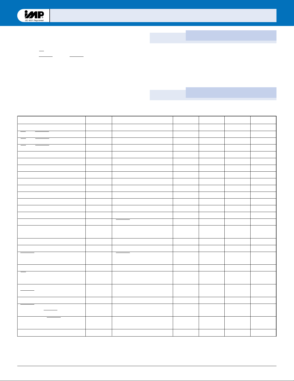
Absolute Maximum Ratings
Electrical Characteristics
Voltage on VCC . . . . . . . . . . . . . . . . . . . . . . . . –0.5V to 7V
Voltage on ST, TD . . . . . . . . . . . . . . . . . . . . . – 0.5V to V
CC
+ 0.5V
Voltage on PBRST, RESET, RESET . . . . . . . . – 0.5V to V
CC
+ 0.5V
Operating Temperature Range . . . . . . . . . . . –40°C to 85°C
Soldering Temperature . . . . . . . . . . . . . . . . . . 260°C for 10 seconds
Storage Temperature . . . . . . . . . . . . . . . . . . . –55°C to 125°C
Voltages measured with respect to ground.
These are stress ratings only and functional operation is not implied.
Parameter Symbol Conditions Min Typ Max Units
Supply Voltage (VCC)V
CC
1.0 5.5 V
ST and PBRST Input High Level V
IH
VCC≥ 2.7V 2 VCC+ 0.3V V
ST and PBRST Input High Level V
IH
VCC< 2.7V VCC- 0.4V V
ST and PBRST Input Low Level V
IL
–0.3 0.5 V
VCCTrip Point (TOL = GND) V
CCTP
2.80 2.88 2.97 V
VCCTrip Point (TOL = VCC)V
CCTP
2.47 2.55 2.64 V
Watchdog Time-Out Period t
TD
TD = GND 62.5 150 250 ms
Watchdog Time-Out Period t
TD
TD = V
CC
500 1200 2000 ms
Watchdog Time-Out Period t
TD
TD floating 250 610 1000 ms
Output Voltage V
OH
I = –500µA, VCC< 2.7V VCC- 0.3V VCC- 0.1V V
Output Current I
OH
Output = 2.4V, VCC≥ 2.7V 350 µA
Output Current I
OL
Output = 0.4V, VCC≥ 2.7V 10 mA
Input Leakage I
IL
–1.0 1.0 µA
RESET Low Level V
OL
0.4 V
Internal Pull-Up Resistor PBRST pin 40 kΩ
Operating Current I
CC1
Outputs open. VCC≤ 3.6V 20 µA
and all inputs at VCCor GND
Input Capacitance C
IN
5pF
Output Capacitance C
OUT
7pF
PBRST Manual Reset t
PB
PBRST = V
IL
20 ms
Minimum Low Time
Reset Active Time t
RST
250 610 1000 ms
ST Pulse Width t
ST
Must not exceed tRDminimum. 20 ns
Watchdog cannot be disabled.
VCCFail Detect to t
RPD
Pulses < 2µs at V
CCTP
58µs
RESET or RESET minimum will not cause reset.
VCCSlew Rate t
F
20 µs
PBRST Stable LOW to t
PDLY
20 ms
RESET and RESET Active
VCCDetect to RESET or t
RPU
t
rise
= 5µs 250 610 1000 ms
RESET Inactive
VCCSlew Rate t
R
0ns
Unless otherwise stated, 1.2V ≤ VCC≤ 5.5V and over the operating temperature range of –40°C to +85°C . All voltages are referenced
to ground.
Page 4

On power-down, once VCCfalls below the reset threshold RESET
stays LOW and is guaranteed to be 0.4V or less until V
CC
drops
below 1.2V. The active HIGH reset signal is valid down to a V
CC
level of 1.2V also.
Manual Reset Operation
Push-button switch input, PBRST, allows the user to override the
internal trip point detection circuits and issue reset signals. The
pushbutton input is debounced and is pulled HIGH through an
internal 40kΩ resistor.
When PBRST is held LOW for the minimum time t
PB
, both resets
become active and remain active for a minimum time period of
250ms after PBRST returns HIGH.
The debounced input is guaranteed to recognize pulses greater
than 20ms. No external pull-up resistor is required, since PBRST
is pulled HIGH by an internal 40kΩ resistor.
The PBRST can be driven from a TTL or CMOS logic line or shorted to ground with a mechanical switch.
ecnareloT
tceleSecnareloT
)V(egatloVtnioPPIRT
niMlanimoNxaM
V=LOT
CC
%0274.255.246.2
DNG=LOT%0108.288.279.2
spe.20t2381
4
408-432-9100/www.impweb.com
©
1999 IMP, Inc.
IMP1
IMP1
832
832
Application Information
Supply Voltage Monitor
The IMP1832 monitors the microprocessor or microcontroller
power supply and issues reset signals, both active HIGH and
active LOW, that halt processor operation whenever the power
supply voltage levels are outside a predetermined tolerance.
Tolerance levels are set with the TOL pin.
RESET and RESET signals are generated at the last moment of a
valid V
CC
signal. On power-up, both reset signals are active for a
minimum of 250ms after the supply has returned to intolerance
level. This allows the power supply and monitored processor to
stabilize before instruction execution is allowed to begin.
Trip Point Tolerance Selection
With TOL connected to V
CC
, RESET and RESET become active
whenever V
CC
falls below 2.64V. RESET and RESET become active
when V
CC
falls below 2.98V if TOL is connected to ground.
After V
CC
has risen above the trip point set by TOL, RESET and
RESET remain active for a minimum time period of 250ms.
Figure 1. Timing Diagram: Power Up
Figure 2. Timing Diagram: Power Down
1832_04.eps
V
CCTP(MAX)
V
CCTP
V
CCTP(MIN)
V
CC
RESET
RESET
t
R
t
RPU
V
OH
V
OL
Figure 3. Timing Diagram: Pushbutton Reset
V
IH
V
IL
V
OH
V
OL
RESET
RESET
PBRST
t
PDLY
t
PB
t
RST
1832_07.eps
Figure 4. Application Circuit: Pushbutton Reset
1832_05.eps
PBRST
Supply
Voltage
1
V
CC
TD
2
ST
TOL
IMP1832
µP
3
4
RESET
GND
8
7
6
5
RESET
RESET
V
CCTP(MAX)
V
CCTP
V
CCTP(MIN)
V
CC
RESET
RESET
t
F
V
OH
V
OL
t
RPD
1832_03.eps
Page 5

Watchdog Timer and ST Input
A watchdog timer stops and restarts a microprocessor that is
“hung-up”. Through the time delay input, TD, three watchdog
time-out periods are selectable: 150ms, 610ms and 1,200ms. If the
strobe input, ST , is not str obed LOW prior to timeout, r eset signals
become active. On power-up or after the supply voltage returns to
an in-tolerance condition, the reset signal remains active for
250ms minimum, allowing the power supply and system microprocessor to stabilize.
ST Pulses as short as 20ns can be detected.
Figure 5. Timing Diagram: Strobe Input
ST
Valid
Strobe
Valid
Strobe
Invalid
Strobe
t
RST
t
ST
Note: ST is ignored whenever a reset is active.
t
TD
(Min)
t
TD
(Max)
1832_08.eps
©
1999 IMP, Inc. 408-432-9100/www.impweb.com 5
IMP1
IMP1
832
832
Application Information
Figure 6. Application Circuit: Watchdog Timer
A HIGH-to-LOW ST signal transition must be regularly issued
no later than the minimum time-out period defined by the state of
the TD signal. This guarantees the watchdog timer does not
time-out.
Timeouts periods of approximately 150ms, 610ms or 1,200ms are
selected through the TD pin.
1832_06.eps
PBRST
Supply
Voltage
1
V
CC
TD
2
ST
TOL
IMP1832
m
P Decoder
3
4
RESET
GND
8
7
6
5
RESET
MREQ
Address
Bus
RESET
leveLegatloVDT
)sm(doirePtuO-emiTgodhctaW
niMlanimoNxaM
DNG5.26051052
gnitaolF0520160001
V
CC
00500210002
spe.30t_2381
The watchdog timer can not be disabled. It must be strobed with
a high-to-low transition to avoid a watchdog timeout and reset.
Page 6

IMP1
IMP1
832
832
Package Dimensions
6
408-432-9100/www.impweb.com
©
1999 IMP, Inc.
Plastic DIP (8-Pin)
L
0°– 8°
C
H
E
e
D
B
A1
A
SO (8-Pin).eps
SO (8-Pin)
MicroSO (8-Pin)
e
b
D
E1 E
a
L
+
C
D
0.10mm
0.004in
A1
A2
A
MicroSO (8-Pin).eps
sehcnIsretemilliM
niMxaMniMxaM
*)niP-8(OSorciM
A ––––– 3340.0 –––– 01.1
1A0200.09500.0050.051.0
2A5920.04730.057.059.0
b8900.07510.052.004.0
C1500.01900.031.032.0
D2411.00221.009.201.3
eCSB6520.0CSB56.0
ECSB391.0CSB09.4
1E2411.00221.009.201.3
L7510.06720.004.007.0
a °0 °6 °0 °6
**)niP-8(OS
A350.0960.053.157.1
1A400.0010.001.052.0
B310.0020.033.015.0
C700.0010.091.052.0
e050.072.1
E051.0751.008.300.4
H822.0442.008.502.6
L610.0050.004.072.1
D981.0791.008.400.2
***)niP-8(PIDcitsalP
A ––––– 012.0 –––– 33.5
1A510.0 ––––– 83.0 –––––
2A511.0591.029.259.4
b410.0220.063.065.0
2b540.0070.041.187.1
3b030.0540.008.041.1
D553.0004.020.961.01
1D500.0 ––––– 31.0 –––––
E003.0523.026.762.8
1E042.0082.001.611.7
e001.0 ––––– 45.2
Ae003.0 ––––– 26.7
Be ––––– 034.0 ––––– 29.01
Ce ––––– 060.0
L511.0051.029.218.3
** AA781-OMgniwarDCEDEJ*
* AA211-SMgniwarDCEDEJ**
AB100-SMgniwarDCEDEJ***
3ta.40t_2381
A2
A
L
A1
D1
D
e
b
b2
0°–15°
E
E1
C
eA
eB
Plastic DIP (8-Pin)a.eps
Page 7

IMP1
IMP1
832
832
IMP, Inc.
Corporate Headquarters
2830 N. First Street
San Jose, CA 95134-2071
Tel: 408-432-9100
Tel: 800-438-3722
Fax: 408-434-0335
e-mail: info@impinc.com
http://www.impweb.com
The IMP logo is a registered trademark of IMP, Inc.
All other company and product names are trademarks of their respective owners.
© 1999 IMP, Inc.
Printed in USA
Publication #: 1015
Revision: B
Issue Date: 11/08/99
Type: Preliminary
 Loading...