

Datasheet IMP1232LPSN, IMP1232LPS-2, IMP1232LPS, IMP1232LPN, IMP1232LPCMA Datasheet (IMP)
...Page 1
©
1999 IMP, Inc. 408-432-9100/www.impweb.com 1
Key Features
◆
Pin compatible with the Dallas Semiconductor
DS1232LP/1232LPS
— 40% lower supply current
◆
5V supply monitor
◆
Selectable watchdog period
◆
Debounce manual push-button reset input
◆
Precision temperature-compensated voltage
reference and comparator
◆
Power-up, power-down and brownout detection
◆
250ms reset time
◆
Active LOW open-drain reset and active HIGH
push-pull output
◆
Selectable trip point tolerance: 5% or 10%
◆
Low-cost, surface mount packages: 8/16-pin
SO, 8-pin DIP and 8-pin MicroSO
◆
Wide operating temperature –40°C to +85°C
(N/EPA suffixed devices)
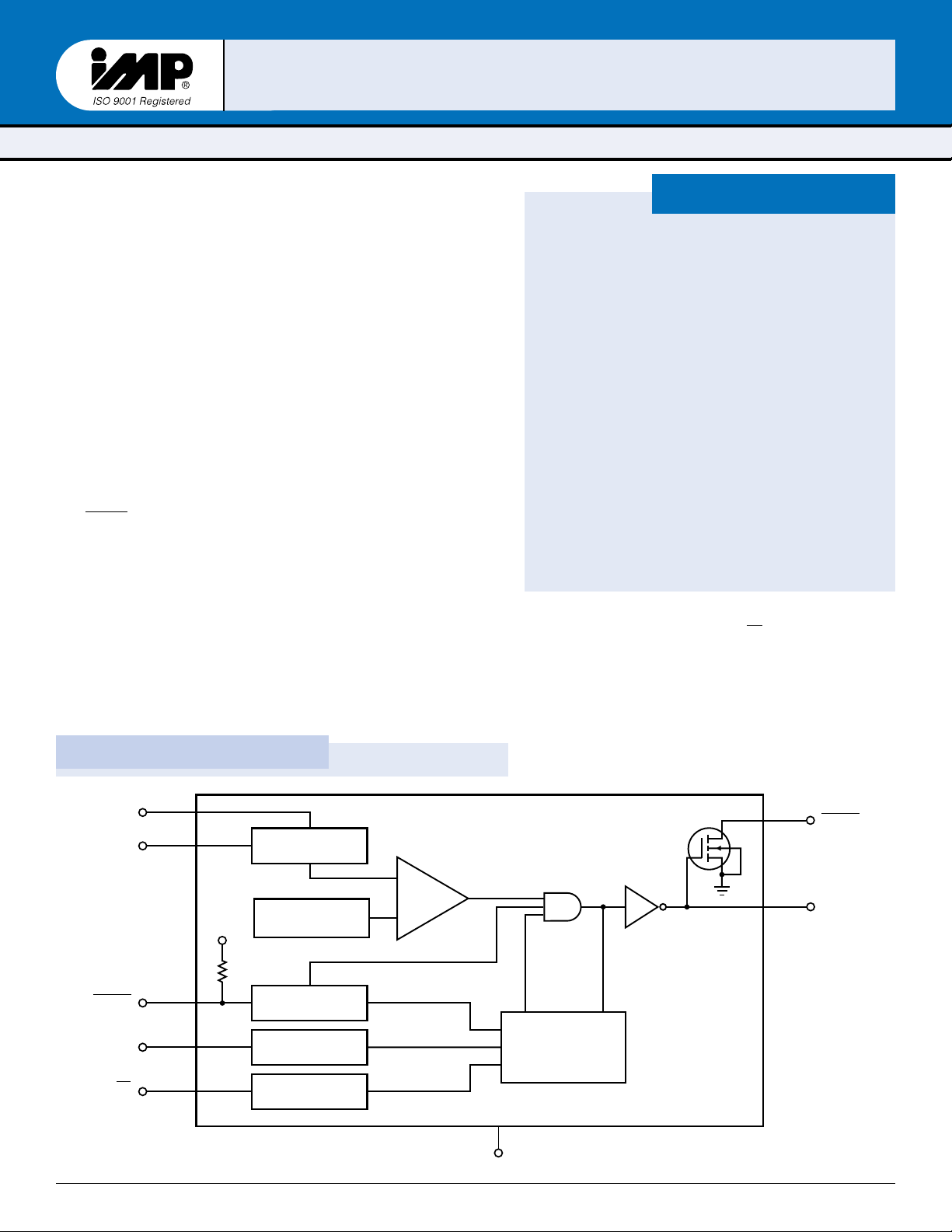
Block Diagram
IMP1
IMP1
232LP/LPS
232LP/LPS
POWER MANAGEMENT
5V
5V µµ
P P
P Pooww
er Suppl
er Suppl
y Monit
y Monit
or and
or and
RReset Cir
eset Cir
cuit
cuit
– Select
– Select
able T
able Trriipp-P-P
oint T
oint T
oler
oler
ance
ance
and W
and W
atc
atc
hdog P
hdog Perer
iod
iod
– Push-Butt
– Push-Butt
on R
on R
eset
eset
The IMP1232LP/LPS microprocessor supervisor can halt and restart a
“hung-up” or “stalled” microprocessor, restart a microprocessor after a
power failure, and debounce and interface a manual push-button microprocessor reset switch. The low-power supervisors feature 40% lower
supply current than the pin compatible Dallas Semiconductor
DS1232LP/LPS.
Precision temperature compensated reference and comparator circuits
monitor the 5V, V
CC
input voltage. During power-up or when the V
CC
power supply falls outside selectable tolerance limits, both the RESET
and RESET become active. When V
CC
rises above the threshold voltage,
the reset signals remain active for an additional 250ms minimum,
allowing the power supply and system microprocessor to stabilize. The
trip point tolerance signal, TOL, selects the trip level tolerance to be
either 5- or 10-percent.
Each device has both a push-pull, active HIGH reset output and an open
drain, active LOW reset output.
A debounced manual reset input activates the reset outputs for a minimum period of 250ms.
Also included is a watchdog timer to stop and restart a microprocessor
that is “hung-up”. Three watchdog time-out periods are selectable:
150ms, 610ms and 1,200ms. If the ST input is not strobed
LOW before the time-out period expires, a reset is issued.
Devices are available in 8-pin DIP, 8/16-pin SO and compact 8-pin MicroSO packages.
CC
TD
ST
8 (15)
3 (6)
1 (2)
2 (4)
7 (13)
V
CC
40kΩ
Timebase Selection
5%/10% Tolerance
Selection
Reference
Push Button
Debounce
Watchdog
Watchdog
Transition Detector
IMP1232LP/LPS
(16-Pin Package)
+
–
Reset &
Watchdog Timer
4 (8)
GND
V
TOL
PBRST
6 (11)
5 (9)
RESET
RESET
1232_03.eps
Page 2

2
408-432-9100/www.impweb.com
©
1999 IMP, Inc.
Pin Configuration
IMP1
IMP1
232LP/LPS
232LP/LPS
Pin Descriptions
Ordering Information
1232_02.eps
IMP1232LPSN
13
ST
14 NC
15 V
CC
16
4
3
2
1NC
TD
12 NC5NC
11 RESET6TOL
10 NC7NC
9 RESET8GND
NC
PBRST
NC
DIP/SO/MicroSO SO
rebmuNtraPegakcaP
erutarepmeTgnitarepO
egnaR
ylppuSmumixaM
(tnerruC µ )A
gnirotinoMegatloV
noitacilppA
PL2321PMIPID-80C° 07otC° 03V5
SPL2321PMIOS-610C° 07otC° 03V5
2-SPL2321PMIOS-80C° 07otC° 03V5
AMCPL2321PMIOSorciM-80C° 07otC° 03V5
AMEPL2321PMIOSorciM-804– C° 58otC° 03V5
NPL2321PMIPID-804– C° 58otC° 03V5
2-NSPL2321PMIOS-804– C° 58otC° 03V5
NSPL2321PMIOS-6104– C° 58otC° 03V5
spe.10t_2321
Pin Number Pin Number
8-Pin P
8-Pin Pacackkagagee11
6-Pin P
6-Pin Pacackkagagee
NName
ame
FFunction
unction
1 2 PBRST Debounced manual pushbutton RESET input
2 4 TD Watchdog time delay selection. (t
TD
= 150ms for TD = GND, tTD= 610ms
for TD = Open, and tTD=1200ms for TD = VCC)
3 6 TOL Selects 5% (TOL connected to GND) or 10% (TOL connected to V
CC
) trip
point tolerance
4 8 GND Ground
5 9 RESET Active HIGH reset output. RESET is active:
1. If VCCfalls below the reset voltage trip point.
2. IfPBRST is LOW.
3. If ST is not strobed LOW before the timeout period set by TD expires.
4. During power-up.
6 11 RESET Active LOW reset output. (See RESET)
7 13 ST Strobe Input
815V
CC
5V power
— 1, 3, 5, 7, 10, NC No internal connection
12, 14, 16
PBRST
1V
IMP1232LP
2
TD
IMP1232LPS-2
IMP1232LPCMA
3
TOL
GND
IMP1232LPEMA
4
8
CC
7ST
6 RESET
5
RESET
1232_01.eps
Page 3
©
1999 IMP, Inc. 408-432-9100/www.impweb.com 3
IMP1
IMP1
232LP/LPS
232LP/LPS
Absolute Maximum Ratings
Electrical Characteristics
Voltage on VCC . . . . . . . . . . . . . . . . . . . . . . . . –0.5V to 7V
Voltage on ST, TD . . . . . . . . . . . . . . . . . . . . . –0.5V to V
CC
+ 0.5V
Voltage on PBRST, RESET, RESET . . . . . . . . –0.5V to V
CC
+ 0.5V
Operating Temperature Range . . . . . . . . . . . – 40°C to 85°C
(N/EMA version)
0°C to 70°C
Soldering Temperature . . . . . . . . . . . . . . . . . . 260°C for 10 seconds
Storage Temperature . . . . . . . . . . . . . . . . . . . –55°C to 125°C
Voltages measured with respect to ground.
These are stress ratings only and functional operation is not implied.
Parameter Symbol Conditions Min Typ Max Units
Supply Voltage (VCC)V
CC
4.5 5.5 V
ST and PBRST Input High Level V
IH
2V
CC
+ 0.3V V
ST and PBRST Input Low Level V
IL
–0.3 0.8 V
VCCTrip Point (TOL = GND) V
CCTP
4.50 4.62 4.74 V
VCCTrip Point (TOL = VCC)V
CCTP
4.25 4.37 4.49 V
Watchdog Time-Out Period t
TD
TD = GND 62.5 150 250 ms
Watchdog Time-Out Period t
TD
TD = V
CC
500 1200 2000 ms
Watchdog Time-Out Period t
TD
TD floating 250 610 1000 ms
Output Voltage V
OH
I = –500µA, Note 3 VCC- 0.5V VCC- 0.1V V
Output Current I
OH
Output = 2.4V , Note 2 – 8 –10 mA
Output Current I
OL
Output = 0.4V, 10 mA
Input Leakage I
IL
Note 1 –1.0 1.0 µA
RESET Low Level V
OL
0.4 V
Internal Pull-Up Resistor Note 1 40 kΩ
Operating Current (CMOS) I
CC1
30 µA
Input Capacitance C
IN
5pF
Output Capacitance C
OUT
10 pF
PBRST Manual Reset t
PB
PBRST = V
IL
20 ms
Minimum Low Time
Reset Active Time t
RST
250 610 1000 ms
ST Pulse Width t
ST
Note 4 20 ns
VCCFail Detect to t
RPD
58µs
RESET or RESET
VCCSlew Rate t
F
4.75V to 4.25V 300 µs
PBRST Stable LOW to t
PDLY
20 ms
RESET and RESET Active
V
CC
Detect to RESET or t
RPU
t
RISE
= 5µs 250 610 1000 ms
RESET Inactive
VCCSlew Rate t
R
4.25V to 4.75V 0 ns
Unless otherwise stated, 4.5V ≤ VCC≤ 5.5V and over the operating temperature range of 0°C to +70°C (–40°C to +85°C for N/EMA
devices). All voltages are referenced to ground.
Notes: 1. PBRST is internally pulled HIGH to VCCthrough a nominal 40kΩ resistor.
2. RESET is an open drain output.
3. RESET remains within 0.5V of V
CC
on power-down until VCCfalls below 2V. RESET remains within 0.5V of ground on power-down
until V
CC
falls below 2.0V.
4. Must not exceed the minimum watchdog time-out period (t
TD
). The watchdog circuit cannot be disabled. To avoid a reset, ST must be
strobed.
Page 4

4
408-432-9100/www.impweb.com
©
1999 IMP, Inc.
IMP1
IMP1
232LP/LPS
232LP/LPS
Application Information
Supply Voltage Monitor
Reset Signal Polarity and Output Stage Structure
RESET is an active LOW signal. It is developed with an open
drain driver. If a pullup resistor is required, typical values are
10kΩ to 50kΩ.
RESET is an active High signal developed by a CMOS push-pull
output stage and is the logical opposite to RESET.
Trip Point Tolerance Selection
With TOL connected to V
CC
, RESET and RESET become active
whenever V
CC
falls below 4.5V. RESET and RESET become active
when V
CC
falls below 4.75V if TOL is connected to ground.
After V
CC
has risen above the trip point set by TOL, RESET and
RESET remain active for a minimum time period of 250ms.
On power-down, once V
CC
falls below the reset threshold RESET
stays LOW and is guaranteed to be 0.4V or less until V
CC
drops
below 1.2V. The active HIGH reset signal is valid down to a V
CC
level of 1.2V also.
Figure 1. Timing Diagram: Power Up
Figure 2. Timing Diagram: Power Down
1232_05.eps
4.75V
V
CCTP
4.25V
V
CC
RESET
RESET
t
R
t
RPU
V
OH
V
OL
Figure 3. Timing Diagram: Pushbutton Reset
V
IH
V
IL
V
OH
V
OL
RESET
RESET
PBRST
t
PDLY
t
PB
t
RST
1232_08.eps
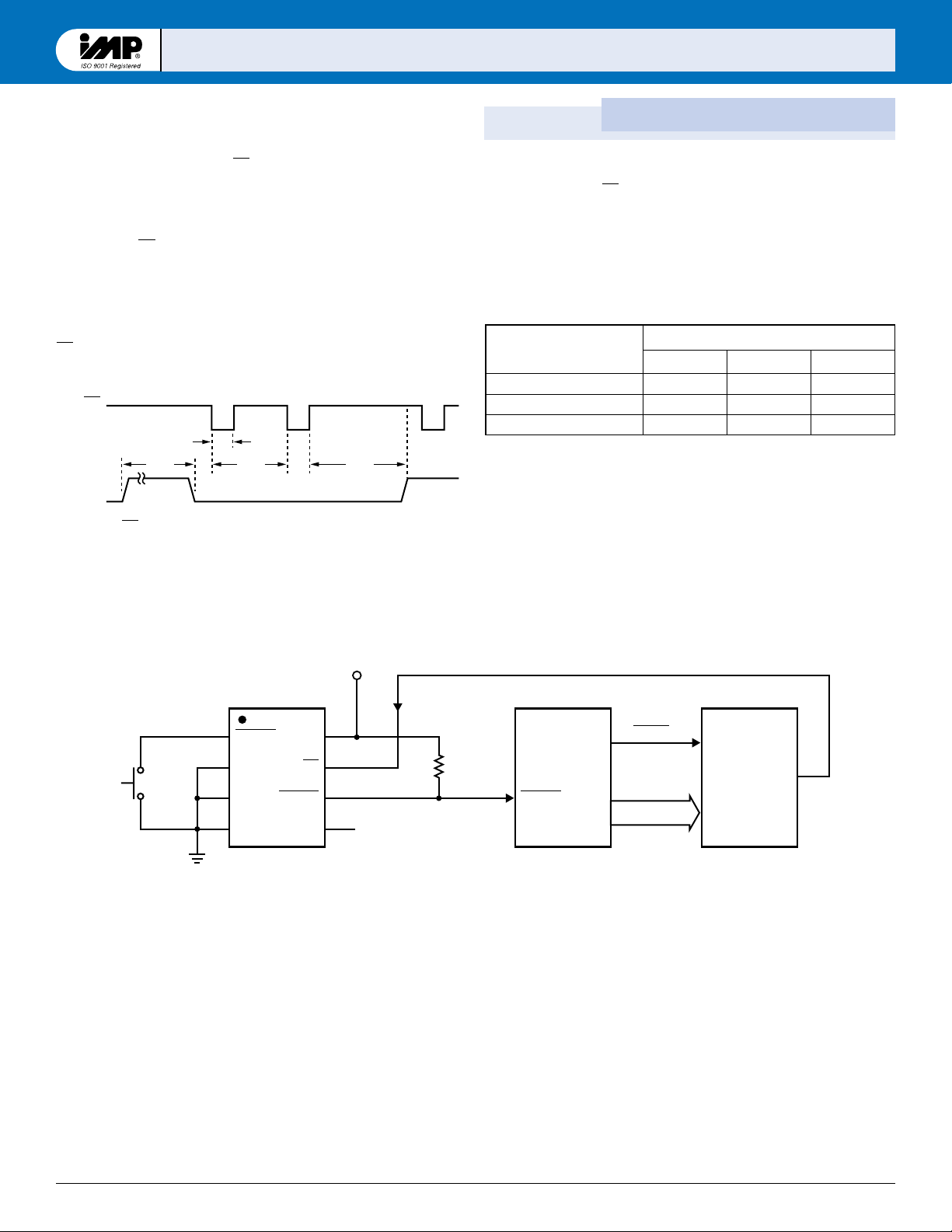
Figure 4. Application Circuit: Pushbutton Reset
1232_06.eps
PBRST
5V
1
V
CC
TD
2
ST
TOL
IMP1232LP/LPS
µP
3
4
RESET
GND
8
7
6
5
RESET
RESET
4.75V
V
CCTP
4.25V
V
CC
RESET
RESET
t
F
V
OH
V
OL
t
RPD
1232_04.eps
Manual Reset Operation
Push-button switch input, PBRST, allows the user to override the
internal trip point detection circuits and issue reset signals. The
pushbutton input is debounced and is normally pulled HIGH
through an internal 40kΩ resistor.
When PBRST is held LOW for the minimum time t
PB
, both resets
become active and remain active for approximately a minimum
time period of 250ms after PBRST returns HIGH.
The debounced input is guaranteed to recognize pulses greater
than 20ms. No external pull-up resistor is required, since PBRST
is pulled HIGH by an internal 40kΩ resistor.
The PBRST can be driven from a TTL or CMOS logic line or shorted to ground with a mechanical switch.
ecnareloT
tceleSecnareloT
)V(egatloVtnioPPIRT
niMlanimoNxaM
V=LOT
CC
%0152.473.494.4
DNG=LOT%55.426.447.4
spe.20t_2321
Page 5
©
1999 IMP, Inc. 408-432-9100/www.impweb.com 5
IMP1
IMP1
232LP/LPS
232LP/LPS
Application Information
Figure 6. Application Circuit: Watchdog Timer
Watchdog Timer and ST Input
A watchdog timer stops and restarts a microprocessor that is
“hung-up”. Through the time delay input, TD, three watchdog
time-out periods are selectable: 150ms, 610ms and 1,200ms. If the
strobe input, ST , is not str obed LOW prior to timeout, r eset signals
become active. On power-up or after the supply voltage returns to
an in-tolerance condition, the reset signal remains active for
250ms minimum, allowing the power supply and system microprocessor to stabilize.
ST Pulses as short as 20ns can be detected.
Figure 5. Timing Diagram: Strobe Input
RESET
ST
Valid
Strobe
Valid
Strobe
Invalid
Strobe
t
RST
t
ST
Note: ST is ignored whenever a reset is active.
t
TD
(Min)
t
TD
(Max)
1232_09.eps
A HIGH-to-LOW ST signal transition must be regularly issued
no later than the minimum time-out period defined by the state of
the TD signal. This guarantees the watchdog timer does not
time-out.
Timeouts periods of approximately 150ms, 610ms or 1,200ms are
selected through the TD pin.
1232_07.eps
PBRST
5V
1
10kΩ
V
CC
TD
2
ST
TOL
IMP1232LP/LPS
µP Decoder
3
4
RESET
GND
8
7
6
5
RESET
MREQ
Address
Bus
RESET
leveLegatloVDT
)sm(doirePtuO-emiTgodhctaW
niMlanimoNxaM
DNG5.26051052
gnitaolF0520160001
V
CC
00500210002
spe.30t_2321
The watchdog timer cannot be disabled. It must be strobed with a
high-to-low transition to avoid a watchdog timeout.
Page 6

IMP1
IMP1
232LP/LPS
232LP/LPS
Package Dimensions
6
408-432-9100/www.impweb.com
©
1999 IMP, Inc.
Plastic DIP (8-Pin)
L
0°– 8°
C
H
E
e
D
B
A1
A
SO (8-Pin).eps
SO (8-Pin)
MicroSO (8-Pin)
e
b
D
E1 E
a
L
+
C
D
0.10mm
0.004in
A1
A2
A
MicroSO (8-Pin).eps
sehcnIsretemilliM
niMxaMniMxaM
*)niP-8(OSorciM
A ––––– 3340.0 –––– 01.1
1A0200.09500.0050.051.0
2A5920.04730.057.059.0
b8900.07510.052.004.0
C1500.01900.031.032.0
D2411.00221.009.201.3
eCSB6520.0CSB56.0
ECSB391.0CSB09.4
1E2411.00221.009.201.3
L7510.06720.004.007.0
a °0 °6 °0 °6
**)niP-8(OS
A350.0960.053.157.1
1A400.0010.001.052.0
B310.0020.033.015.0
C700.0010.091.052.0
e050.072.1
E051.0751.008.300.4
H822.0442.008.502.6
L610.0050.004.072.1
D981.0791.008.400.2
***)niP-8(PIDcitsalP
A ––––– 012.0 –––– 33.5
1A510.0 ––––– 83.0 –––––
2A511.0591.029.259.4
b410.0220.063.065.0
2b540.0070.041.187.1
3b030.0540.008.041.1
D553.0004.020.961.01
1D500.0 ––––– 31.0 –––––
E003.0523.026.762.8
1E042.0082.001.611.7
e001.0 ––––– 45.2
Ae003.0 ––––– 26.7
Be ––––– 034.0 ––––– 29.01
Ce ––––– 060.0
L511.0051.029.218.3
** AA781-OMgniwarDCEDEJ*
* AA211-SMgniwarDCEDEJ**
AB100-SMgniwarDCEDEJ***
3ta.40t_2321
A2
A
L
A1
D1
D
e
b
b2
0°–15°
E
E1
C
eA
eB
Plastic DIP (8-Pin)a.eps
Page 7

IMP1
IMP1
232LP/LPS
232LP/LPS
IMP, Inc.
Corporate Headquarters
2830 N. First Street
San Jose, CA 95134-2071
Tel: 408-432-9100
Tel: 800-438-3722
Fax: 408-434-0335
e-mail: info@impinc.com
http://www.impweb.com
The IMP logo is a registered trademark of IMP, Inc.
All other company and product names are trademarks of their respective owners.
© 1999 IMP, Inc.
Printed in USA
Publication #: 1011
Revision: B
Issue Date: 11/08/99
Type: Preliminary
Package Dimensions
SO (16-Pin)
H
E
eB
D
A1
A
L
0°– 8°
C
SO (14-Pin).eps
sehcnIsretemilliM
niMxaMniMxaM
*)niP-61(OS
A629.03401.053.256.2
1A0400.08110.001.003.0
B310.0020.033.015.0
C1900.05210.032.023.0
D7793.03314.001.0105.01
E4192.02662.004.706.7
eCSB050.0CSB72.1
H493.0914.000.0156.01
L610.0050.004.072.1
AA310-SMgniwarDCEDEJ*
3ta.30t_62/4252
 Loading...