

Datasheet ILC7262CS-50-33, ILC7262CS-50-30, ILC7262CS-33-30 Datasheet (Impala Linear Corporation)
Page 1
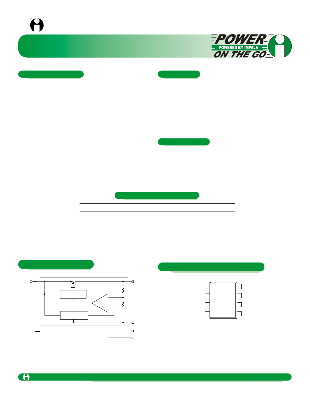
Dual 125mA CMOS LDO in an SO-8 package. This part
offers 120mV dropout voltage on each output at 100mA typical (5V part), and nearly zero dropout below 5mA. Each
output is independently short-circuit protected.
Its all-CMOS design means that only 2.2µA of current is
required to run the part.
±2% accurate outputs come in a number of configurations,
to allow for flexible yet compact portable system designs.
ILC7262
Dual CMOS LDO
Impala Linear Cor poration
Impala Linear Corporation
1
(408) 574-3939
www.impalalinear.com
June 1996
ILC7262 1.0
• All-CMOS design in an 8-lead SOIC package
• ±2% precision outputs
• 2.2µA of Iq
• Short-circuit protected outputs
• Voltage options allow:
Dual 50mA 5.0 & 3.3V Regulator
Dual 50mA 5.0 & 3.0V Regulator
Dual 125mA 5V to 3.0V & 3.3V Convertor
• Battery-powered Equipment
• Portable communications
• PDAs and palmtops
ILC7262CS-50/30
Dual 50mA 5v & 3.0V Regulator
ILC7262CS-50/33
Dual 50mA 5V & 3.3V Regulator
ILC7262CS-33/30
Dual 125mA 5V to 3.0 V & 3.3V Converter
*Standard Product offering comes in tape & reel, quantity 1000 per reel, orientation right.
REFERENCE VOLTAGE
SOURCE
V
OUT
1
V
IN
-
+
SHORT-CIRCUIT
PROTECT
V
SS
V
OUT
2
VSS2
NC
V
SS
1
V
SS
2
NC
V
IN
V
OUT
1
V
OUT
2
NC
1
2
3
45
6
7
8
SO-8
(TOP VIEW)
Block Diagram
General Description
Features
Applications
Ordering Information
Pin-Package Configurations
Page 2
Dual CMOS LDO
Impala Linear Corporation
2
(408) 574-3939
www.impalalinear.com
June 1996
ILC7262 1.0
Parameter
Symbol
Ratings
Units
Input Voltage
V
IN
12
V
Output Current
I
OUT
500
mA
Output Voltage
V
OUT
VSS-0.3~VIN+0.3
V
Continuous Total
Power Dissipation
Pd 300
mW
Operating Ambient Temperature
T
opr
-30~+80
°C
Storage Temperature
T
stg
-40~+125
°C
Parameter
Symbol
Conditions
Min
Typ
Max
Units
Supply Current
I
SS VIN
= 6.0V
2.2
6.0
µA
Input Voltage
V
IN
10.0
V
Parameter
Symbol
Conditions
Min
Typ
Max
Units
Output Voltage
V
OUT
I
OUT
= 40mA, VIN = 6.0V
4.90
5.0
5.10
V
Maximum Output Current
I
OUT
max
VIN =6.0V, V
OUT
> 4.5V
250
mA
Load Stability
∆V
OUT
VIN = 6.0V, 1mA < I
OUT
< 100mA
40
80
mV
Input/Output
Voltage Differential
V
dif
I
OUT
= 100mA
I
OUT
= 200mA
120
380
300
600
mV
Input Stability
∆V
OUT
∆VIN • V
OUT
I
OUT
= 40mA
6.0V < VIN < 10.0V
0.2
0.3
%/V
Output Voltage
Temperature Characteristics
∆V
OUT
∆T
opr
• V
OUT
I
OUT
= 40mA
-30°C < T
opr
< 80°C
±100
ppm/°C
Note:
1. V
OUT
means the output voltage when “V
OUT
+ 1.0V” is provided at the VINpin while maintaing a certain I
OUT
value.
2. V
dif
is defined as “VIN-V
OUT
” where V
OUT
= V
SET
x 0.98.
Note: The total of I
OUT
’s must be less than Pd/ (VIN-V
OUT
1) + Pd/ (VIN-V
OUT
2)
Absolute Maximum Ratings (TA= 25°C)
Electrical Characteristics
ILC7262 COMMON CHARACTERISTICS TA= 25°C.
Electrical Characteristics ILC7262
V
OUT
SECTION: V
OUT
(T) = 5.0V, TA= 25°C
Page 3

Dual CMOS LDO
Impala Linear Corporation
3
(408) 574-3939
www.impalalinear.com
June 1996
ILC7262 1.0
Parameter
Symbol
Conditions
Min
Typ
Max
Units
Output Voltage
V
OUT
I
OUT
= 40mA, VIN = 6.0V
3.234
3.30
3.37
V
Maximum Output Current
I
OUT
max
VIN = 6.0V, V
OUT
> 2.97V
165
mA
Load Stability
∆V
OUT
VIN = 6.0V, 1mA < I
OUT
< 80mA
45
90
mV
Input/Output
Voltage Differential
V
dif
I
OUT
= 80mA
I
OUT
= 160mA
180
400
360
700
mV
Input Stability
∆V
OUT
∆VIN • V
OUT
I
OUT
= 40mA
6.0V<
VIN < 10.0V
0.2
0.3
%/V
Output Voltage
Temperature Characteristics
∆V
OUT
∆T
opr
• V
OUT
I
OUT
= 40mA
-30°C <
T
opr
< 80°C
±100
ppm/°C
Parameter
Symbol
Conditions
Min
Typ
Max
Units
Output Voltage
V
OUT
I
OUT
= 40mA, VIN = 6.0V
2.94
3.0
3.06
V
Maximum Output Current
I
OUT
max
VIN = 6.0V, V
OUT
> 2.7V
150
mA
Load Stability
∆V
OUT
VIN = 6.0V, 1mA < I
OUT
< 80mA
45
90
mV
Input/Output
Voltage Differential
V
dif
I
OUT
= 80mA
I
OUT
= 160mA
180
400
360
700
mV
Input Stability
∆V
OUT
∆VIN • V
OUT
I
OUT
= 40mA
6.0V< VIN < 10.0V
0.2
0.3
%/V
Output Voltage
Temperature Characteristics
∆V
OUT
∆T
opr
• V
OUT
I
OUT
= 40mA
-30°C < T
opr
< 80°C
±100
ppm/°C
Electrical Characteristics ILC7262
V
OUT
2 SECTION: V
OUT
(T) = 3.3V, TA= 25°C
Electrical Characteristics ILC7262
V
OUT
2 SECTION: V
OUT
(T) = 3.0V, TA= 25°C
Page 4

Dual CMOS LDO
Impala Linear Corporation
4
(408) 574-3939
www.impalalinear.com
June 1996
ILC7262 1.0
OUTPUT VOLTAGE vs OUTPUT CURRENT
OUTPUT VOLTAGE vs INPUT VOLTAGE
OUTPUT VOLTAGE vs INPUT VOLTAGE
OUTPUT VOLTAGE vs INPUT VOLTAGE
LINE TRANSIENT RESPONSE
VDOvs OUTPUT CURRENT
ILC7262CM 3.0V SECTION
ILC7262CM 3.0V SECTION
ILC7262CM 3.0V SECTION
ILC7262CM 3.0V SECTION
ILC7262CM 5.0V SECTION
ILC7262CM 3.0V SECTION
3.1
3.0
2.9
2.8
0 20 40 60 80 100 120 140 160
OUTPUT CURRENT I
OUT
(mA)
OUTPUT VOLTAGE V
OUT
(V)
OUTPUT VOLTAGE V
OUT
(V)
VIN= 4.0V
T
opr
= -30°C
T
opr
= 25°C
T
opr
= 25°C
I
OUT
= 1mA
I
OUT
= 1mA
I
OUT
= 10mA
I
OUT
= 10mA
VIN= 4.0V
Input Voltage
Output Voltage
40mA
40mA
10mA
T
opr
= 25°C
25°C
80°C
80°C
-30°C
0.6
0.5
0.4
0.3
0.2
0.0
-0.2
V
DO
(V)
0 20 40 60 80 100 120 140 160
OUTPUT CURRENT I
OUT
(mA)
3.2
3.0
2.8
2.6
2.4
2.2
2.5 3.0 3.5
INPUT VOLTAGE VIN(V)
T
opr
(°C)
3.2
3.0
2.8
2.6
2.4
2.2
OUTPUT VOLTAGE V
OUT
(V)
3.0 4.0 5.0 6.0 7.0 8.0 9.0 10.0
INPUT VOLTAGE VIN(V)
8.0
7.5
7.0
6.5
6.0
5.5
5.0
4.5
4.0
-1 0 1 2 3
TIME (ms)
(V)
OUTPUT VOLTAGE V
OUT
(V)
3.01
3.00
2.99
2.98
2.97
2.96
2.95
2.94
-40 -20 0 20 40 60 80 100
Typical Performance Characteristics General conditions for all curves
 Loading...