

Datasheet ILC7011C5-50, ILC7011C5-47, ILC7011C5-33, ILC7011C5-30, ILC7011C5-28 Datasheet (Impala Linear Corporation)
...Page 1
The ILC7011 is an 80mA, Ultra Low Noise, Low Dropout
(LDO) linear regulator, designed and processed in Impala’s
proprietary CMOS process technology. This process combines the best CMOS features of low quiescent current,
small size and low dropout voltage with the best bipolar features of high ripple rejection, ultra low noise and power handling capability. The ILC7011 offers a quiescent current of
less than 100µA, a logic level enable (regulator on/off) pin,
a footprint that is half the size of the industry standard SOT23 and a low dropout voltage of 50mV at 10mA. With better than 70dB (1kHz) of ripple rejection, ultra low noise of
10µV
RMS
and 1% output voltage accuracy , the ILC7011 sets
a new standard in linear regulators for communications and
personal electronics applications.
The ILC7011 is designed to operate with small, low cost,
ceramic capacitors and is stable over a wide range of ESR
values. In addition to the output capacitor, the ILC7011
requires only a 1µF input capacitor. The enable pin can be
tied to V
IN
for easy device layout. The ILC7011 is available
in a number of fixed output voltages ranging from 2.5V to
8V. An adjacent version will be available shortly.
The ILC7011 is ideally suited for use in small size cordless
and cellular handsets as well as many other low battery
powered electronic devices. Please contact Impala for
samples and application information.
ILC7011
80mA SC70 Ultra Low Noise CMOS RF-LDO™ Regulator
Impala Linear Cor poration
Impala Linear Corporation
1
(408) 574-3939
www.impalalinear.com
August 2000
ILC7011 1.4
Preliminary
• 1% output voltage accuracy
• Only 10µV
RMS
noise from 300Hz to 100kHz
• Uses low ESR ceramic or Tantalum output capacitor to
minimize noise and output ripple.
• Only 90µA ground current at 80mA load
• Ripple rejection up to 70dB at 1kHz, 60dB at 1MHz
• Excellent line and load transient response
• Guaranteed to 80mA output current
• Industry standard five lead SC70 packages
• Fixed 2.8V, 3.0V, 3.3V, 3.6V, 4.7V, 5.0V, output voltage
options
• Metal mask option available for custom voltages between
2.5V and 8V
• Cellular phones
• Wireless communicators
• PDAs / palmtops / organizers
• Battery powered portable electronics
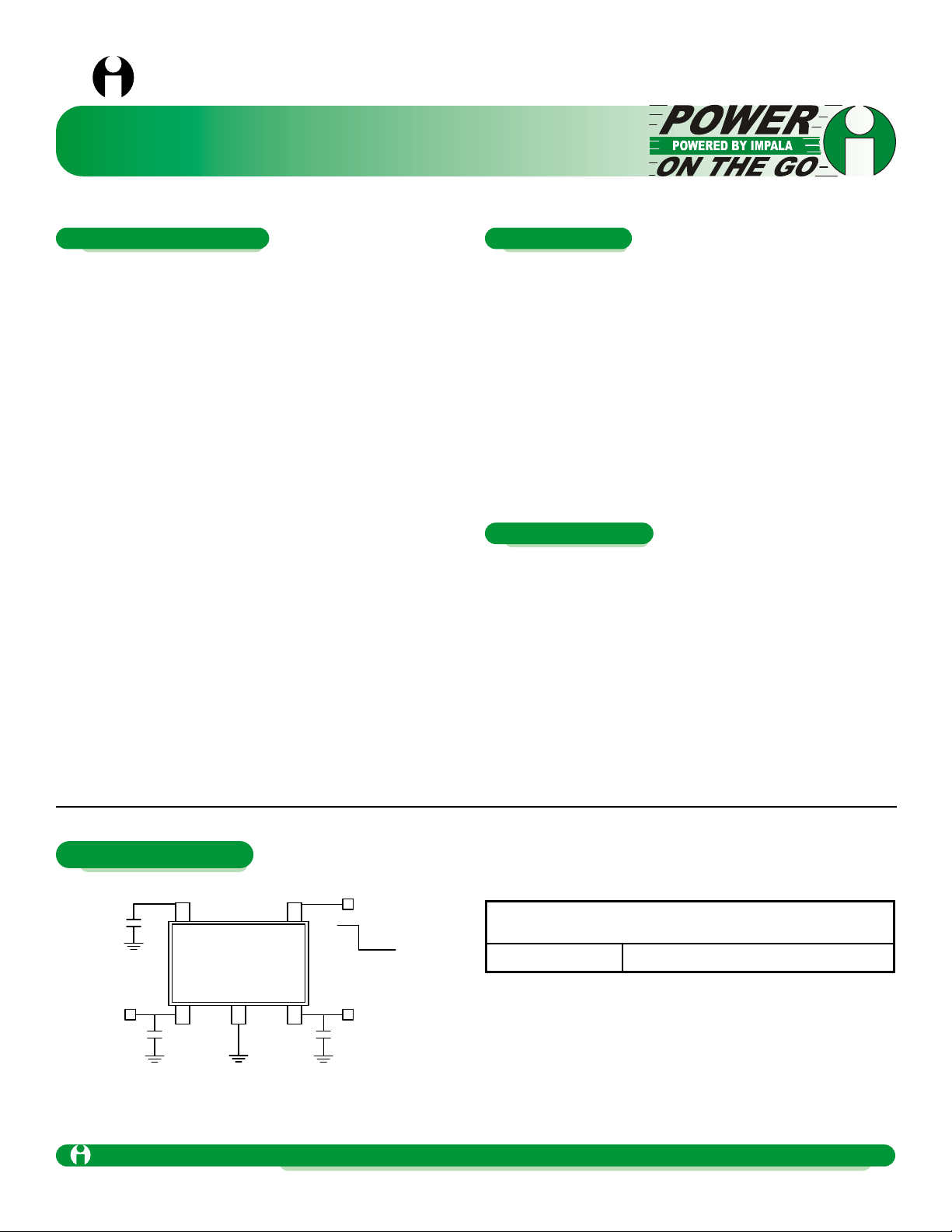
5
ILC7011
ON
OFF
V
IN
C
IN
C
OUT
V
OUT
4
12
3
C
NOISE
Ordering Information
(TA= 0°C to 70°C)
Typical Circuit
ILC7011C5-XX 80mA, fixed voltage, SC-70 Package
Note: Fixed voltage options are defined by 2-digit code as shown
in the package markings information section of the data sheet
General Description
Features
Applications
Page 2
80mA SC 70 Ultra Low Noise CMOS RF-LDO™ Regulator
Impala Linear Corporation
2
(408) 574-3939
www.impalalinear.com
August 2000
ILC7011 1.4
Preliminary
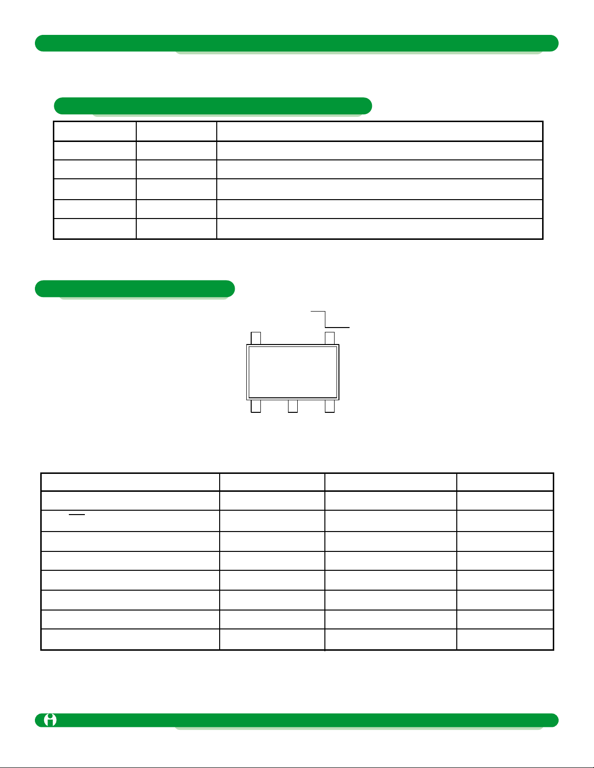
5
ILC7011
V
IN
V
OUT
4
12
3
C
NOISE
ON
OFF
GND
Pin Number
4
5
2
1
2
Pin Name
ON/OFF
C
NOISE
GND
V
OUT
V
IN
Pin Description
By applying less than 0.4V to this pin the device will be turned off
Noise Bypass Capacitor
Ground pin. Local ground for C
OUT
Output voltage. Connect C
OUT
between this pin and the GND (pin 3)
Connect Directly to Supply
Pin Description ILC7011 (fixed voltage version)
Parameter
Input Voltage 7011
ON/OFF Input Voltage
Output Current
Output Voltage
Package Power Dissipation
Maximum Juncion Temp. Range
Storage Temperature
Operation Ambient Temperature
Symbol
V
IN
V
ON/OFF
I
OUT
V
OUT
P
D
T
J(MAX)
T
STG
T
STG
Ratings
-0.3 to +9V
-0.3 to V
IN
Short Circuit Protected
-0.3 to VIN+0.3
TBD
-40 to +125
-40 to +125
-40 to +125
Units
V
V
mA
V
mW
°C
°C
°C
Pin Package Configurations
Page 3

80mA SC 70 Ultra Low Noise CMOS RF-LDO™ Regulator
Impala Linear Corporation
3
(408) 574-3939
www.impalalinear.com
August 2000
ILC7011 1.4
Preliminary
Parameter
Input Voltage Range
Output Voltage Accuracy
Line Regulation
Dropout Voltage (Note 3)
Ground Pin Current
Shutdown (OFF) Current
ON/OFF Input Voltage
ON/OFF Pin Input Current
(Note 5)
Peak Output Current
(Note 4)
Output Noise Voltage
Ripple Rejection
Dynamic Line Regulation
Dynamic Load Regulation
Short Circuit Current
Resistance Shutdown
Discharge
Symbol
V
IN
∆V
OUT/(VOUT
*∆VIN)
V
IN VOUT
I
GND
I
ON/OFF
V
ON/OFF
I
IN ON/OFF
I
OUT (peak)
e
N
∆V
OUT
/∆V
IN
∆V
OUT(line)
∆V
OUT(load)
I
SC
Conditions
V
OUT
(NOM) + 1V <
8V
I
OUT
= 10µA
I
OUT
= 10mA
I
OUT
= 20mA
I
OUT
= 80mA
I
OUT =
0mA
I
OUT
= 10mA
I
OUT
= 80mA
I
ON/OFF
= 0V
High = Regulator On
Low = Regulator Off
V
ON/OFF
0.6V Regulator OFF
V
ON/OFF
2V Regulator ON
V
OUT
> 0.95V
OUT (NOM), tpw
= 2ms
BW = 300Hz to 50kHz, C
IN
= 1µF
C
NOISE
= 0.01µF, C
OUT
= 1.0µF, I
OUT
= 10mA
C
OUT
= 4.7µF Tantalum
I
OUT
= 80mA
VIN: V
OUT (NOM)
+ 1V to V
OUT
(NOM) + 2V, tr/tf = 2µs; I
OUT
= 80mA
I
OUT
: 1mA to 80mA; tr < 5µS
V
OUT
= 0V
Typ
2.5-8
±1
0.007
0.1
50
70
235
66
67
90
0.1
1.5-2.0
0.6
0.3
1
100-120
TBD
70
50
65
14
40
200
1.5
Units
V
%
%/V
mV
µA
µA
V
µA
mA
µVrms
dB
mV
mV
mA
kΩ
Freq = 1kHz
Freq = 10kHz
Freq = 1MHz
Note 1: Absolute maximum ratings indicate limits which when exceeded may result in damage to the component. Electrical specifications do not apply when operating the
device outside of its rated operating conditions.
Note 2: Specified Min/Max limits are production tested or guaranteed through correlation based on statistical control methods. Measurments are taken at constant junction
temperature as close to ambient as possible using low duty pulse testing.
Note 3 Dropout voltage is defined as the input to output differential voltage at which the output voltage drops 2% below the nominal value measured with a 1V differential.
Note 4: Guaranteed by design
Note 5: The device’s shutdown pin inlcudes a 2MΩ internal pull down resistor connected to ground.
Electrical Characteristics ILC7011
Unless otherwise specified all limits are at TA= 25°C, VIN= V
OUT
(NOM) + 1V, I
OUT
= 1mA, C
OUT
= 1mF, V
ON/OFF
= 2V
Page 4

80mA SC 70 Ultra Low Noise CMOS RF-LDO™ Regulator
Impala Linear Corporation
4
(408) 574-3939
www.impalalinear.com
August 2000
ILC7011 1.4
Preliminary
1.15/1.35
.325
.70
.45
.65 .65
1.30
Recommended Mount Pad
1.85
.325
1.80-2.20
0.65 BSC
0.65 BSC
0.15-0.30
c
0.80-1.00
0.78-0.98
0.45-0.60
0.10-0.18
0.02
1.30
x
15°
Output Voltage (V)
2.8
3.0
3.3
3.6
4.7
5.0
Grade
A
A
A
A
A
A
Order Information
ILC7011C5-28
ILC7011C5-30
ILC7011C5-33
ILC7011C5-36
ILC7011C5-47
ILC7011C5-50
Supplied As:
3K Units on Tape and Reel
3K Units on Tape and Reel
3K Units on Tape and Reel
3K Units on Tape and Reel
3K Units on Tape and Reel
3K Units on Tape and Reel
*NOTE: First two characters identify the product and the last two characters identify the datecode
Devices sold by Impala Linear Corporation are covered by the warranty and patent indemnification provisions appearing
in its Terms of Sale only. Impala Linear Corporation makes no warranty, express, statutory, implied, or by description
regarding the information set forth herein or regarding the freedom of the described devices from patent infringement.
Impala Linear Corporation makes no warranty of merchantability or fitness for any purpose. Impala Linear Corporation
reserves the right to discontinue production and change specifications and prices at any time and without notice.
This product is intended for use in normal commercial applications. Applications requiring an extended temperature
range, unusual environmental requirements, or high reliability applications, such as military and aerospace, are specifically not recommended without additional processing by Impala Linear Corporation.
Impala Linear Corporation assumes no responsibility for the use of any circuitry other than circuitry embodied in an
Impala Linear Corporation product. No other circuits, patents, licenses are implied.
Life Support Policy
Impala Linear Corporation’s products are not authorized for use as critical components in life support devices or systems.
1. Life support devices or systems are devices or systems which, (a) are intended for surgical implant into the body, or
(b) support or sustain life, and whose failure to perform, when properly used in accordance with instructions for use provided in the labelling, can be reasonably expected to result in a significant injury to the user.
2. A critical component is any component of a life support device or system whose failure to perform can be reasonbly expected to cause the failure of the life support device or system, or to affect its safety or effectiveness.
SC-70 Package Markings
ILC7011C5-xx
 Loading...