

Page 1

SiC
Silicon Carbide Diode
5th Generation thinQ!
650V SiC Schottky Diode
TM
IDH09G65C5
Final Datasheet
Rev. 2.2, 2012-12-10
Power Management & Multimarket
Page 2
IDH09G65C55th Generation thinQ!™ SiC Schottky Diode
1 Description
ThinQ!™ Generation 5 represents Infineon leading edge technology for the SiC
Schottky Barrier diodes. The Infineon proprietary diffusion soldering process,
already introduced with G3 is now combined with a new, more compact design and
thin-wafer technology. The result is a new family of products showing improved
efficiency over all load conditions, resulting from both the improved thermal
characteristics and a lower figure of merit (Qc x Vf).
The new thinQ!™ Generation 5 has been designed to complement our 650V
CoolMOS™ families: this ensures meeting the most stringent application
requirements in this voltage range.
Features
Revolutionary semiconductor material - Silicon Carbide
Benchmark switching behavior
No reverse recovery/ No forward recovery
Temperature independent switching behavior
High surge current capability
Pb-free lead plating; RoHS compliant
Qualified according to JEDEC
Breakdown voltage tested at 20 mA
Optimized for high temperature operation
1)
for target applications
2)
Benefits
System efficiency improvement over Si diodes
System cost / size savings due to reduced cooling requirements
Enabling higher frequency / increased power density solutions
Higher system reliability due to lower operating temperatures
Reduced EMI
Applications
Switch mode power supply
Power factor correction
Solar inverter
Uninterruptible power supply
Table 1 Key Performance Parameters
Parameter Value Unit
VDC
QC; VR=400V 14 nC
EC; VR=400V 3.2 µJ
IF @ TC < 145°C
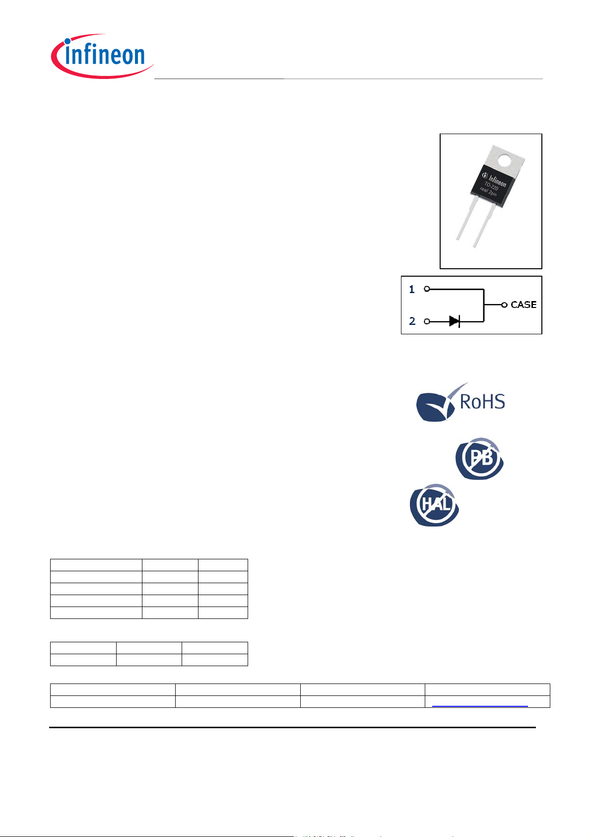
Table 2 Pin Definition
Pin 1 Pin 2 Pin 3
C A n.a.
Type / ordering Code Package Marking Related links
IDH09G65C5 PG-TO220-2 D0965C5 www.infineon.com/sic
650 V
9 A
1
2
1) J-STD20 and JESD22
2) All devices tested under avalanche conditions for a time periode of 10ms
Final Data Sheet 2 Rev. 2.2, 2012-12-10
Page 3

5
th
Generation thinQ!TM SiC Schottky Diode
IDH09G65C5
Table of contents
Table of Contents
1 Description .......................................................................................................................................... 2
2 Maximum ratings ................................................................................................................................ 4
3 Thermal characteristics ..................................................................................................................... 4
4 Electrical characteristics ................................................................................................................... 5
5 Electrical characteristics diagrams .................................................................................................. 6
6 Simplified Forward Characteristics Model ...................................................................................... 8
7 Package outlines ................................................................................................................................ 9
8 Revision History ............................................................................................................................... 10
Final Data Sheet 3 Rev. 2.2, 2012-12-10
Page 4
5
th
Generation thinQ!TM SiC Schottky Diode
IDH09G65C5
Maximum ratings
2 Maximum ratings
Table 3 Maximum ratings
Parameter Symbol Values Unit Note/Test Condition
Min. Typ. Max.
Continuous forward current IF – –
Surge non-repetitive forward current,
sine halfwave
Non-repetitive peak forward current I
i²t value
I
– –
F,SM
– –
– –
F,max
∫ i²dt
– –
– –
Repetitive peak reverse voltage V
Diode dv/dt ruggedness
Power dissipation P
Operating and storage temperature Tj;T
Mounting torque
– –
RRM
dv/dt
– –
tot
-55 –
stg
– –
– –
9
75
65
396
28
21
650
100
82
175
70
TC < 145°C, D=1
A
TC = 25°C, tp=10 ms
TC = 150°C, tp=10 ms
TC = 25°C, tp=10 µs
A²s TC = 25°C, tp=10 ms
TC = 150°C, tp=10 ms
V Tj = 25°C
V/ns VR=0..480 V
W TC = 25°C
°C
Ncm M3 screws
3 Thermal characteristics
Table 4 Thermal characteristics TO-220-2
Parameter Symbol Values Unit Note/Test Condition
Min. Typ. Max.
Thermal resistance, junction-case R
Thermal resistance, junctionambient
Soldering temperature,
wavesoldering only allowed at leads
–
thJC
R
thJA
T
sold
– –
– –
1.1 1.8
K/W
62
260
°C
leaded
1.6mm (0.063 in.) from
case for 10 s
Final Data Sheet 4 Rev. 2.2, 2012-12-10
Page 5

5
th
Generation thinQ!TM SiC Schottky Diode
IDH09G65C5
Electrical characteristics
4 Electrical characteristics
Table 5 Static characteristics
Parameter Symbol Values Unit Note/Test Condition
Min. Typ. Max.
DC blocking voltage VDC
Diode forward voltage V
F
Reverse current IR
Table 6 AC characteristics
Parameter Symbol Values Unit Note/Test Condition
Total capacitive charge Qc
Total Capacitance
C
650 – –
– 1.5 1.7
– 1.8 2.1
– 0.45 160
– 0.1 56
– 1.8 1100
Min. Typ. Max.
–
14
– 270 –
– 35 –
– 35 –
V
µA
nC
pF
IR= 0.16 mA, Tj=25°C
IF= 9 A, Tj=25°C
I
= 9 A, Tj=150°C
F
VR=650 V, Tj=25°C
V
=600 V, Tj=25°C
R
V
=650 V, Tj=150°C
R
VR=400 V, di/dt=200A/µs,
I
F≤IF,MAX
, T
=150°C
j
VR=1 V, f=1 MHz
V
=300 V, f=1 MHz
R
V
=600 V, f=1 MHz
R
Final Data Sheet 5 Rev. 2.2, 2012-12-10
Page 6

5
th
Generation thinQ!TM SiC Schottky Diode
IDH09G65C5
Electrical characteristics diagrams
5 Electrical characteristics diagrams
Table 7
Power dissipation Maximal diode forward current
90
80
70
60
50
[A]
F
I
40
30
20
10
0
25 50 75 100 125 150 175
TC[°C]
; Tj≤175°C; parameter D=duty cycle
thJC,max
0.1
0.3
0.5
0.7
1
P
90
80
70
60
50
[W]
tot
P
40
30
20
10
=f(TC); R
tot
0
25 50 75 100 125 150 175
TC[°C]
IF=f(TC); R
thJC,max
Table 8
Typical forward characteristics Typical forward characteristics in surge current
18
16
-55°C
25°C
14
12
10
[A]
F
8
I
100°C
150°C
175°C
6
4
2
0
00.511.522.53
VF[V]
90
80
70
[A]
F
I
60
50
40
25°C
100°C
30
20
10
0
0123456
VF[V]
IF=f(VF); tp=200 µs; parameter: Tj IF=f(VF); tp=200 µs; parameter: Tj
-55°C
150°C
175°C
Final Data Sheet 6 Rev. 2.2, 2012-12-10
Page 7

5
th
Generation thinQ!TM SiC Schottky Diode
IDH09G65C5
Electrical characteristics diagrams
Table 9
Typ. capacitance charge vs. current slope1) Typ. reverse current vs. reverse voltage
16
14
12
10
[nC]
C
8
Q
6
4
2
0
100 300 500 700 900
dIF/dt [A/µs]
QC=f(diF/dt); Tj=150°C; VR=400 V; IF≤I
1) Only capacitive charge, guaranteed by design.
IR=f(VR); parameter: Tj;
F,max
1.E-5
1.E-6
1.E-7
[A]
R
I
1.E-8
1.E-9
100 200 300 400 500 600
175°C
150°C
100°C
VR[V]
25°C
-55°C
Table 10
Max. transient thermal impedance Typ. capacitance vs. reverse voltage
350
1
300
250
0.5
[K/W]
0.1
th,jc
Z
0.01
1.E-06 1.E-03 1.E+00
tp[s]
Z
=f(tP); parameter: D=tP/T; C=f(VR); Tj=25°C; f=1 MHz
th,jc
0.2
0.1
0.05
0.02
0.01
single pul se
200
150
C [pF]
100
50
0
0 1 10 100 1000
VR[V]
Final Data Sheet 7 Rev. 2.2, 2012-12-10
Page 8

5
th
Generation thinQ!TM SiC Schottky Diode
IDH09G65C5
Electrical characteristics diagrams
Table 11
Typ. capacitance stored energy
9
8
7
6
5
[µJ]
C
E
4
3
2
1
0
0 200 400 600
VR[V]
EC=f(VR)
6 Simplified Forward Characteristics Model
Table 12
Equivalent forward current curve Mathematical Equation
IRVV
FDIFFTHF
TTV
jjTH
[A]
F
I
V
th
1/R
VF[V]
diff
6-
VF=f(IF) Tj in °C; -55°C < Tj < 175°C; IF < 18 A
V 04.1001.0
2
4-
TTTR
jjjDIFF
0.05210.43110.431
Final Data Sheet 8 Rev. 2.2, 2012-12-10
Page 9

5th Generation thinQ!TM SiC Schottky Diode
IDH09G65C5
Package outlines
7 Package outlines
Figure 1 Outlines TO-220, dimensions in mm/inches
Final Data Sheet 9 Rev. 2.2, 2012-12-10
Page 10

5th Generation thinQ!TM SiC Schottky Diode
th
IDH09G65C5
Revision History
8 Revision History
5
Generation thinQ!TM SiC Schottky Diode
Revision History: 2012-12-10, Rev. 2.2
Previous Revision:
Revision Subjects (major changes since last version)
2.0 Release of the final datasheet.
2.1 Reverse current values, maximum diode forward voltage.
2.2 Reverse current values, tested avalanche current, simplified calculation model
We Listen to Your Comments
Any information within this document that you feel is wrong, unclear or missing at all?
Your feedback will help us to continuously improve the quality of this document.
Please send your proposal (including a reference to this document) to: erratum@infineon.com
Edition 2012-12-10
Published by
Infineon Technologies AG
81726 Munich, Germany
© 2012 Infineon Technologies AG
All Rights Reserved.
Legal Disclaimer
The information given in this document shall in no event be regarded as a guarantee of conditions or
characteristics. With respect to any examples or hints given herein, any typical values stated herein and/or any
information regarding the application of the device, Infineon Technologies hereby disclaims any and all
warranties and liabilities of any kind, including without limitation, warranties of non-infringement of intellectual
property rights of any third party.
Information
For further information on technology, delivery terms and conditions and prices, please contact the nearest
Infineon Technologies Office (www.infineon.com).
Warnings
Due to technical requirements, components may contain dangerous substances. For information on the types in
question, please contact the nearest Infineon Technologies Office.
The Infineon Technologies component described in this Data Sheet may be used in life-support devices or
systems and/or automotive, aviation and aerospace applications or systems only with the express written
approval of Infineon Technologies, if a failure of such components can reasonably be expected to cause the
failure of that life-support, automotive, aviation and aerospace device or system or to affect the safety or
effectiveness of that device or system. Life support devices or systems are intended to be implanted in the
human body or to support and/or maintain and sustain and/or protect human life. If they fail, it is reasonable to
assume that the health of the user or other persons may be endangered.
Final Data Sheet 10 Rev. 2.2, 2012-12-10
Page 11

www.infineon.com
Published by Infineon Technologies AG
 Loading...