

Page 1
HVB27WK
Variable Capacitance Diode for FM tuner
ADE-208-594 (Z)
Features
• High capacitance ratio.
• Low series resistance.(rs=0.4 max)
• Good linearity of C-V curve.
• To be usable at low voltagee.
• CMPAK package is suitable for high density surface mounting and high speed assembly.
Ordering Information
Type No. Laser Mark Package Code
HVB27WK T5 CMPAK
Rev 0
Apr. 1998
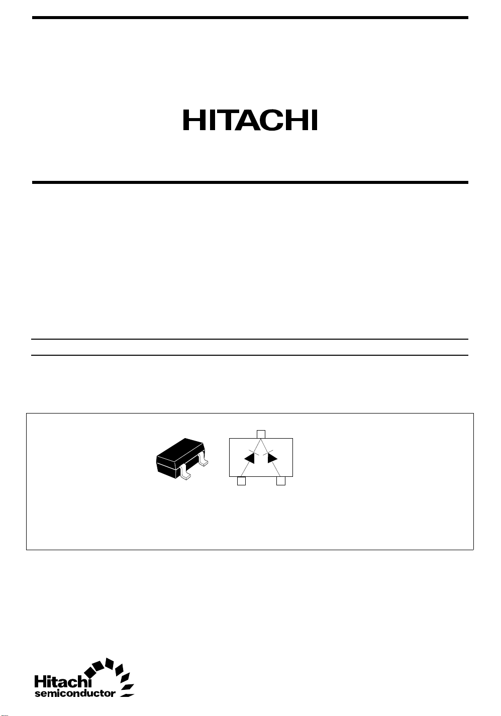
Outline
3
2
(Top View)
1
1 Anode
2 Anode
3 Cathode
Page 2
HVB27WK
Absolute Maximum Ratings (Ta = 25°C)
*1
Item Symbol Value Unit
Reverse voltage V
R
15 V
Junction temperature Tj 125 °C
Storage temperature Tstg –55 to +125 °C
Notes: 1. Per one device.
Electrical Characteristics (Ta = 25°C)
*3
Item Symbol Min Typ Max Unit Test Condition
Reverse current I
Capacitance C
Capacitance ratio n
Series resistance r
R1
I
R2
1
C
2
C
8
1
n
2
s
Matching error ∆C/C*
— — 10 nA VR =9V
— — 100 VR =9V, Ta = 60°C
52.0 — 62.0 pF VR = 1V, f = 1 MHz
43.0 — 48.0 VR = 2V, f = 1 MHz
24.0 — 28.0 VR = 8V, f = 1 MHz
1.80 — — — C1/ C
1.70 — — C2/ C
8
8
— — 0.40 Ω VR = 2V, f = 100MHz
1
— — 3.0 % VR = 1 to 8V, f = 1 MHz
Notes: 1. A set of HVB27WK is of uniform C-V characteristics.
Measure max. value and min. value of capacitance at each bias point of V
Calculate Matching Error,
∆C/C = × 100 (%)
(Cmax – Cmin)
Cmin
2. Each group shall uniform a multiple of 4 diodes.
3. Per one device.
= 1V through 8V.
R
2
Page 3

Main Characteristic
–6
10
–7
10
–8
10
R
–9
10
–10
10
–11
Reverse current I (A)
10
–12
10
–13
10
0 5 10 15
Reverse voltage V (V)
HVB27WK
R
Fig.1 Reverse current Vs. Reverse voltage
60
f=1MHz
50
40
30
20
Capacitance C (pF)
@@
10
0
1.0
Reverse voltage V (V)
Fig.2 Capacitance Vs. Reverse voltage
10
R
40
3
Page 4

HVB27WK
Package Dimensions
Laser Mark
+ 0.1
0.3
– 0.05
0.65
2.0 ± 0.2
3
T 5
2
1.3 ± 0.2
Unit : mm
+ 0.1
0.3
– 0.05
1
0.3
+ 0.1
– 0.05
0.65
0.425
1.25 ± 0.1
0.425
2.1 ± 0.3
0.16
0 - 0.1
+ 0.1
– 0.06
1 Anode
2 Anode
3 Cathode
0.2
0.9 ± 0.1
Hitachi Code
JEDEC Code
EIAJ Code
Weight (g)
CMPAK
—
SC-70
0.006
4
Page 5

HVB27WK
Cautions
1. Hitachi neither warrants nor grants licenses of any rights of Hitachi’s or any third party’s patent,
copyright, trademark, or other intellectual property rights for information contained in this document.
Hitachi bears no responsibility for problems that may arise with third party’s rights, including
intellectual property rights, in connection with use of the information contained in this document.
2. Products and product specifications may be subject to change without notice. Confirm that you have
received the latest product standards or specifications before final design, purchase or use.
3. Hitachi makes every attempt to ensure that its products are of high quality and reliability. However,
contact Hitachi’s sales office before using the product in an application that demands especially high
quality and reliability or where its failure or malfunction may directly threaten human life or cause risk
of bodily injury, such as aerospace, aeronautics, nuclear power, combustion control, transportation,
traffic, safety equipment or medical equipment for life support.
4. Design your application so that the product is used within the ranges guaranteed by Hitachi particularly
for maximum rating, operating supply voltage range, heat radiation characteristics, installation
conditions and other characteristics. Hitachi bears no responsibility for failure or damage when used
beyond the guaranteed ranges. Even within the guaranteed ranges, consider normally foreseeable
failure rates or failure modes in semiconductor devices and employ systemic measures such as failsafes, so that the equipment incorporating Hitachi product does not cause bodily injury, fire or other
consequential damage due to operation of the Hitachi product.
5. This product is not designed to be radiation resistant.
6. No one is permitted to reproduce or duplicate, in any form, the whole or part of this document without
written approval from Hitachi.
7. Contact Hitachi’s sales office for any questions regarding this document or Hitachi semiconductor
products.
Hitachi, Ltd.
Semiconductor & IC Div.
Nippon Bldg., 2-6-2, Ohte-machi, Chiyoda-ku, Tokyo 100-0004, Japan
Tel: Tokyo (03) 3270-2111
Fax: (03) 3270-5109
For further information write to:
Hitachi Semiconductor
(America) Inc.
2000 Sierra Point Parkway
Brisbane, CA. 94005-1897
U S A
Tel: 800-285-1601
Fax:303-297-0447
Hitachi Europe GmbH
Continental Europe
Dornacher Straße 3
D-85622 Feldkirchen
München
Tel: 089-9 91 80-0
Fax: 089-9 29 30-00
Hitachi Europe Ltd.
Electronic Components Div.
Northern Europe Headquarters
Whitebrook Park
Lower Cookham Road
Maidenhead
Berkshire SL6 8YA
United Kingdom
Tel: 01628-585000
Fax: 01628-585160
Hitachi Asia Pte. Ltd.
16 Collyer Quay #20-00
Hitachi Tower
Singapore 049318
Tel: 535-2100
Fax: 535-1533
Copyright © Hitachi, Ltd., 1998. All rights reserved. Printed in Japan.
Hitachi Asia (Hong Kong) Ltd.
Unit 706, North Tower,
World Finance Centre,
Harbour City, Canton Road
Tsim Sha Tsui, Kowloon
Hong Kong
Tel: 27359218
Fax: 27306071
5
 Loading...