

Page 1
OTP CMOS 256K×8-Bit EPROM
Features
•
Operating voltage: +5.0V
•
Programming voltage
–
VPP=12.5V±0.2V
–
VCC=6.0V±0.2V
•
High-reliability CMOS technology
•
Latch-up immunity to 100mA from -1.0V to
V
+1.0V
CC
•
CMOS and TTL compatible I/O
•
Low power consumption
–
Active: 30mA max.
–
Standby: 1µA typ.
•
256K×8-bit orga nization
General Description
The HT27C020 chip family is a low-power,
2048K (2,097,152) bit, +5V electrically one-time
programmable (OTP) read-only memories
(EPROM). Organized in to 256K words with 8
bits per word, it fea tures a fast single addres s
location programming, typically at 75
byte. Any byte can be accessed in less than
µs per
HT27C020
•
Fast read access time: -70ns, -90ns
and -120ns
•
Fast programming algorithm
•
Programming time 75µs typ.
•
Two line controls (OE and CE)
•
Standard product identification code
•
Package type
–
32-pin DIP/SOP
–
32-pin PLCC
•
Commercial temperature range
(0
°C to +70°C)
70ns/90ns/120ns with respect to Spec. This
eliminates the need for WAIT states in highperformance microprocessor systems. The
HT27C020 has separate Output Enable (
and Chip Enable (
CE) controls which eliminate
bus contention issues.
OE)
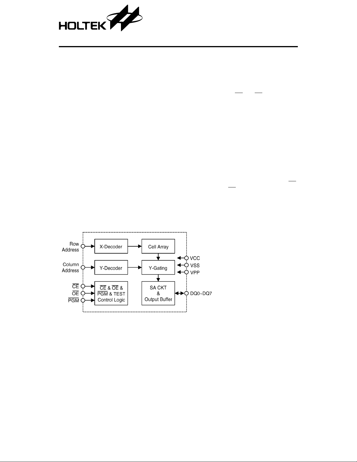
Block Diagram
1 10th May ’99
Page 2
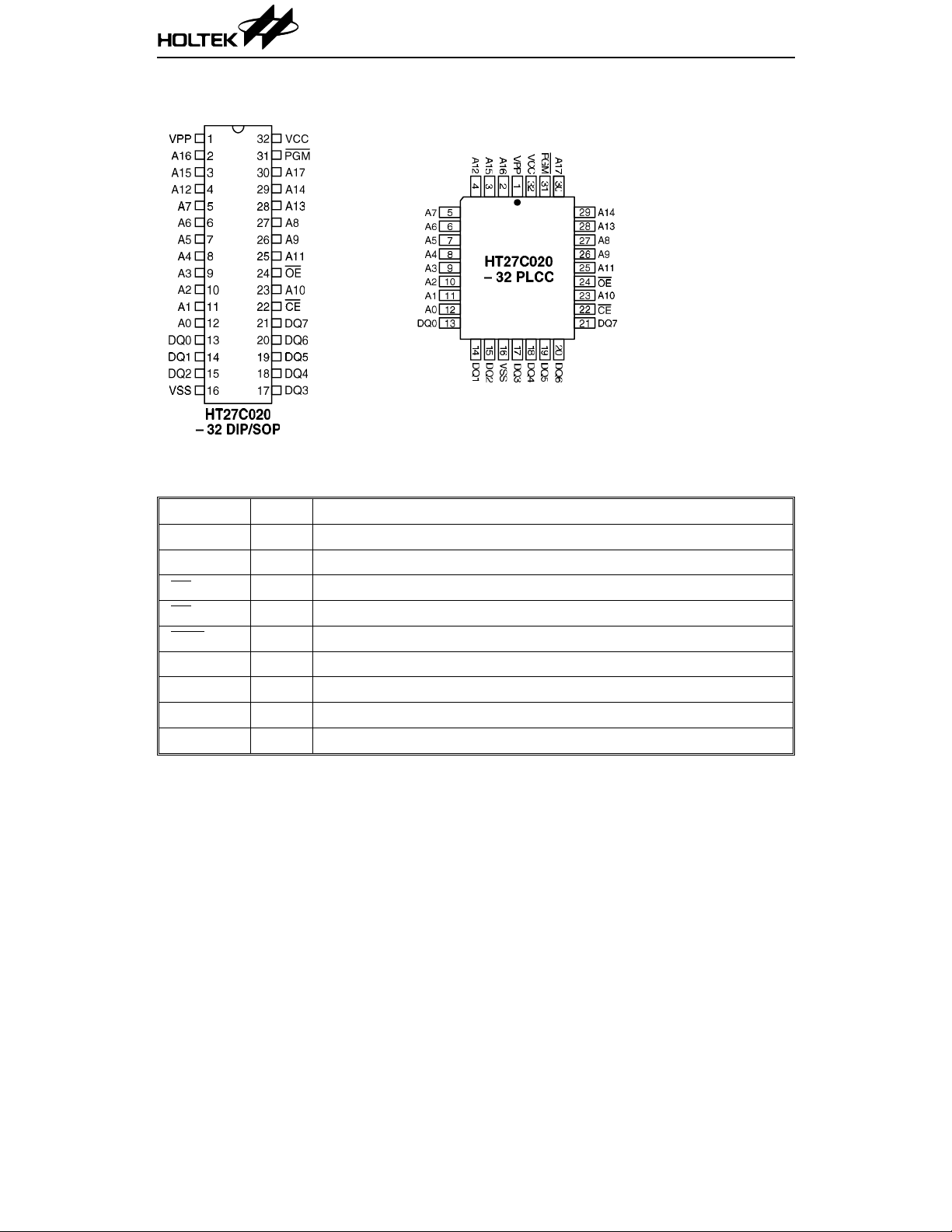
Pin Assignment
Pin Description
HT27C020
Pin Name I/O/C/P Description
A0~A17 I Address inputs
DQ0~DQ7 I/O Data inputs/outputs
CE C Chip enable
OE C Output enable
PGM C Program strobe
NC — No connection
VPP P Program voltage supply
VCC I Positive power supply
VSS I Negative power supply
2 10th May ’99
Page 3
HT27C020
Absolute Maximum Rating
Operation Temperature Commercial ............................................................................ ......0°C to +70°C
Storage Temperature................................ .... .... .... .... .... .... .... .... .... .... .... .... .... .... .... .... .... ....–65
Applied VCC V olt age with Respect to VSS..................... ............ .. ............ ............ ............ –0.6V to 7.0V
Applied Voltage on Input Pin with Respect to VSS.......................................................... –0.6V to 7.0V
Applied Voltage on Output Pin with Respect to VSS.............................................. –0.6V to V
Applied Voltage on A9 Pin with Respect to VSS .......................................... .... .. .. .... .. .. .. –0.6V to 13.5V
Applied VPP Voltage with Respect to VSS ............................... .... .... .... .... .... .... .... .... .... ...–0.6V to 13.5V
Applied READ Voltage (Functionality is guaranteed between these limits) ...............+4.5V to +5.5V
Note: These are stres s ratings only. Stresses exceeding the range specified under “Absolute Maxi-
mum Ratings” may cause substantial damage to the device. Functional operation of this device
at other conditions beyond those listed in the specification is not implied and prolonged
exposure to extreme condition s may affect device reliability.
D.C. Characteristics
Read operation
Symbol Parameter
V
V
V
V
I
LI
I
LO
I
CC
I
SB1
I
SB2
I
PP
Output High Level 5V IOH=–0.4mA 2.4 — — V
OH
Output Low Level 5V IOL=2.1mA — — 0.45 V
OL
Input High Level 5V — 2.0 — VCC+0.5 V
IH
Input Low Level 5V — –0.3 — 0.8 V
IL
Input Leakage Current 5V VIN=0 to 5.5V –5 — 5
Output Leakage Current 5V V
VCC Active Current 5V
Standby Current (CMOS) 5V
Standby Current (TTL) 5V CE=V
VPP Read/Standby Current 5V CE=OE=VIL, VPP=V
Test Conditions
V
CC
OUT
CE=VIL, f=5MHz,
I
OUT
CE=V
Conditions
Min. Typ. Max. Unit
=0 to 5.5V –10 — 10
=0mA
±0.3V
CC
IH
—— 30 mA
— 1.0 10
— — 1.0 mA
—— 100
CC
°C to 125°C
+0.5V
CC
µA
µA
µA
µA
3 10th May ’99
Page 4
Programming operation
Symbol Parameter
V
OH
V
OL
V
IH
V
IL
I
LI
V
H
I
CC
I
PP
Output High Level 6V IOH=–0.4mA 2.4 — — V
Output Low Level 6V IOL=2.1mA — — 0.45 V
Input High Level 6V — 0.7V
Input Low Level 6V — –0. 5 — 0.8 V
Input Load Current 6V VIN=VIL, V
A9 Product ID Voltage 6V — 11.5 — 12.5 V
VCC Supply Current 6V — — — 40 mA
VPP Supply Current 6V CE=V
Capacitance
Symbol Parameter
C
C
C
IN
OUT
VPP
Input Capacitance 5V VIN=0V — 8 12 pF
Output Capacitance 5V V
VPP Capacitance 5V VPP=0V — 18 25 pF
Test Conditions
V
CC
Conditions
IL
Test Conditions
V
CC
HT27C020
Min. Typ. Max. Unit
—VCC+0.5 V
CC
IH
Conditions
=0V — 8 12 pF
OUT
— — 5.0
——10mA
Min. Typ. Max. Unit
µA
A.C. Characteristics
Read operation
Symbol Parameter
t
t
t
t
t
Address to Output Delay 5V CE=OE=VIL— 70 — 90 — 120 ns
ACC
Chip Enable to Output
CE
Delay
Output Enable to Output
OE
Delay
CE or OE High to Output
Float, Whichever
DF
Occurred First
Output Hold from
OH
Address,
CE or OE,
Whichever Occurred First
Test Conditions –70 –90 –120
Unit
VCCConditions Min. Max. Min. Max. Min. Max.
5V
5V
OE=V
CE=V
IL
IL
— 70 — 90 — 120 ns
—30—35—40ns
5V — — 25 — 25 — 30 ns
5V — 0—0—0—ns
4 10th May ’99
Page 5

HT27C020
Programming operation
Symbol Parameter
t
t
t
t
t
t
t
t
t
t
t
t
AS
OES
DS
AH
DH
DFP
VPS
PW
VCS
CES
OE
PRT
Address Set up Time 6V — 2 — —
OE Setup Time 6V — 2 — —
Data Setup Time 6V — 2 — —
Address Hold Tim e 6V — 0 — —
Data Hold Time 6V — 2 — —
Output Enable to Output Float
Delay
VPP Setup Time 6V — 2 — —
PGM Program Pulse Width 6V — 30 75 105
VCC Setup Time 6V — 2 — —
CE Setup Time 6V — 2 — — ns
Data Valid from OE 6V — — — 150
VPP Pulse Rise Time Dur ing
Programming
Test waveforms and measurements
For -70, -90, -120 devices:
Ta=+25°C±5°C
Test Conditions
V
CC
Conditions
Min. Typ. Max. Unit
6V — 0 — 130 ns
6V — 2 — —
µs
µs
µs
µs
µs
µs
µs
µs
µs
µs
tR, tF< 20ns (10% to 90%)
Output test load
Note: CL=100pF including jig capacitance, except for the
-45 devices, where C
5 10th May ’99
=30pF .
L
Page 6

Functional Description
HT27C020
Programming of the HT27C020
When the HT27C 020 is delivere d, the chi p has
all 2048K bits in the “ONE”, or HIGH state.
“ZEROs” are loaded into the HT27C020 through
programming.
The programming mode is entered when
12.5
±0.2V is applied to the VPP pin, OE is at V
and
CE and PGM are VIL. For programming, the
IH
data to be programmed is applied with 8 bits in
parallel to the data pins.
The programming flowchart in Figure 3
shows the fast interactive programming algorithm. The interactive algorithm reduces programming time by using 30
µs to 105µs
programming pulses and giving each address
only as many pulses as is necessary in order to
reliably program the data. After each pulse is
applied to a given address, the data in that
address is verified. If the data is not verified,
additional pulses are given until it is verified
or until the maximum number of pulses is
reached while sequencing through each address of the HT27C020. This process is repeated while sequencing through each address
of the HT27C020. This part of the programming algorithm is done at V
=6.0V to assure
CC
that each EPROM bit is programmed to a sufficiently high threshold voltage. This ensures
that all bits have sufficient margin. After the
final address is completed, the entire EPROM
memory is read at V
CC=VPP
=5.25±0.25V to ver-
ify the entire memory .
Program inhibit mode
Programming of multiple HT27C020 in parallel
with different data is also easily accomplished by
using the Program Inhibit Mode. Except for
CE,
all like inputs of the parallel HT27C020 may be
common. A TTL lo w-level pro gram puls e appl ied to
an HT27C020
LOW, an d
A high-level
CE input with Vpp=12.5±0.2V, PGM
OE HIGH will program that HT27C020.
CE input inhibits the HT27C020 from
being programmed.
Program verify mode
Verification should be performed on the programmed bits to determine whether they were
correctly programm ed. The verifica tion should
be performed with
V
, and VPP at its programming voltage.
IH
,
Auto product identification
OE and CE at VIL, PGM at
The Auto Product Identification mode allows
the reading out of a binary code from an
EPROM that will identify its manufacturer and
the type. This mode is intended for progra mming to automatica lly match the device to be
programmed with its corresponding programming algorith m. Th is m od e is fun ctio na l in th e
25
°C±5°C ambient temperature range that is
required when programming the HT27C020.
To activate this mode, the programming equip-
ment must force 12.0
±0.5V on the address line A9
of the HT27C020. Two identifier bytes may then
be sequenced from the device outputs by toggling
address line A0 from V
to VIH, when A1=VIH. All
IL
other address lines must be held at V
Auto Product Identification mode.
Byte 0 (A0=V
code, and byte 1 (A0=V
) represents the ma nufacturer
IL
), the device co de. For
IH
HT27C020, these two identifier bytes are given in
the Operation mode truth table. All identifiers for
the manufacturer and device codes will possess
odd parity, with the MSB (DQ7) defined as the
parity bit. Wh en A1=V
, the HT27C020 will read
IL
out the binary code of 7F, continuation code, to
signify the unavailability of manufacturer ID
codes.
Read mode
The HT27C0 20 h as two co ntro l fun ctio ns, bo th
of which must be logica lly satisfie d in orde r to
obtain data at outputs. Chip Enable (
power control and should be used for device
selection. Output Enable (
OE) is the output
control and should be used to gate data to th e
output pins, independent of device selection.
Assuming that addresses are stable, address
access time (t
) is equal to the delay from CE
ACC
during
IH
CE) is the
6 10th May ’99
Page 7

HT27C020
to output (tCE). Data is available at the outputs
(t
) after the falling edge of OE, assuming the
OE
CE has been LOW and addresses have been
stable for at least t
ACC-tOE
.
Standby mode
The HT27C020 has CMOS standby mode which
reduces the maximum VCC curren t to 10
is placed in CMOS standby when
V
±0.3V. The HT27C020 also has a TTL-
CC
µA. It
CE is at
standby mode which reduces the maximum
VCC current to 1.0mA. It is placed in TTLstandby when
CE is at VIH. When in standby
mode, the outputs are in a high-impedance
state, independent of the
OE input.
Two-line output control function
To accommodate multiple memory connections,
a two-line contro l functi on is provid ed to allow
for:
•
Low memory power dissipation
•
Assurance that output bus contention will not
occur
It is recommended that
CE be decoded an d used
as the primary device-se lection fun ction, while
OE be made a common connection to the READ
line from the system control bus. Th is assures
that all deselected me mo ry de vices are in the ir
low-power standby mode and that the output
pins are only active when data is desired from a
particular memory device.
System considerations
During the switch betwe en active and standby
conditions, transient current peaks are produced on th e rising and falling edges of Chip
Enable. The magnitud e of these transient current peaks is dependent on the output capacitance loading of the device. At a minimum, a
0.1
µF ceramic capacitor (high frequency, low
inherent inductance) should be used on each
device between VCC and VPP to minimize transient effects. In addition, to overcom e the voltage drop caused by the inductive effects of the
printed circuit board traces on EPROM arrays,
a 4.7
µF bulk electrolytic capacitor should be
used between VCC and VPP for each eight devices. The location of the capacitor should be
close to where the power supply is connected to
the array.
Operation mode truth table
All the operation modes are shown in the table following.
Mode CE OE PGM A0 A1 A9 VPP Output
Read V
Output Disable V
Standby (TTL) V
Standby (CMOS)
V
Program V
Program Verify V
Product Inhi bi t V
Manufacturer Code (3) V
Device Type Code (3) V
Notes:
= 12.0V ± 0.5V
(1) V
H
(2) X=Either V
IH
or V
CC
IL
IL
IL
IH
± 0.3V
IL
IL
IH
IL
IL
V
V
X (2) X X X V
IL
IH
XXXXVCCHigh Z
XXXX XVCCHigh Z
XXXX XV
V
V
IH
IL
V
IL
V
IH
XXXVPPD
XXXVPPD
XXXX XVPPHigh Z
V
IL
V
IL
XVILV
XVIHV
IH
IH
VH (1) V
VH (1) V
(3) For Manufacturer Code and Device Code, A1=VIH, When A1=VIL, both codes will read 7F
7 10th May ’99
CC
CC
CC
CC
Dout
High Z
IN
OUT
1C
02
Page 8

Product Identification Code
HT27C020
Code
Manufacturer 0 1 000111001C
Device Type 1 1 0000001002
Continuation
A0 A1 DQ7 DQ6 DQ5 DQ4 DQ3 DQ2 DQ1 DQ0
00011111117F
10011111117F
Figure 1. A.C. waveforms for read operation
Pins
Hex
Data
8 10th May ’99
Page 9

HT27C020
Figure 2. Programming waveforms
9 10th May ’99
Page 10

HT27C020
Figure 3. Fast programming flowchart
10 10th May ’99
Page 11

HT27C020
Holtek Semiconductor Inc. (Headquarters)
No.3 Creation Rd. II, Science-based Industrial Park, Hsinchu, Taiwan, R.O.C.
Tel: 886-3-563-1999
Fax: 886-3-563-1189
Holtek Semiconductor Inc. (Taipei Office)
5F, No.576, Sec.7 Chung Hsiao E. Rd., Taipei, Taiwan, R.O.C.
Tel: 886-2-2782-9635
Fax: 886-2-2782-9636
Fax: 886-2-2782-7128 (International sales hotline)
Holtek Microelectronics Enterprises Ltd.
RM.711, Tower 2, Cheung Sha Wan Plaza, 833 Cheung Sha Wan Rd., Kowloon, Hong Kong
Tel: 852-2-745-8288
Fax: 852-2-742-8657
Copyright © 1999 by HOLTEK SEMICONDUCTOR INC.
The information appearing in this Data Sheet is believed to be accurate at the time of publication. However, Holtek
assumes no responsibility arising from the use of the specif ications descri bed. The applications mentioned herein are
used solely for the purpose of illustration and Holtek makes no warranty or representation that such applications
will be suitable without further modification, nor recommends the use of its products for appli cation that may present
a risk to human life due to malfunction or otherwise. Holtek reserves the right to alter its products without prior
notification. For the most up-to-date information, please visit our web site at http://www.holtek.com.tw.
11 10th May ’99
 Loading...