

Page 1
Features
·
VFD display 12 hour clock function
·
4.194304MHz crystal oscillation
·
Zero adjust function
General Description
The HT16561 provides direct drive to VFD panels to im
plement a 12 hour clock function. In addition to obtaining
its time base from a 4.194304MHz crystal oscillation
source and in having a wide operating voltage, the de
vice also contains a host of other features. These in
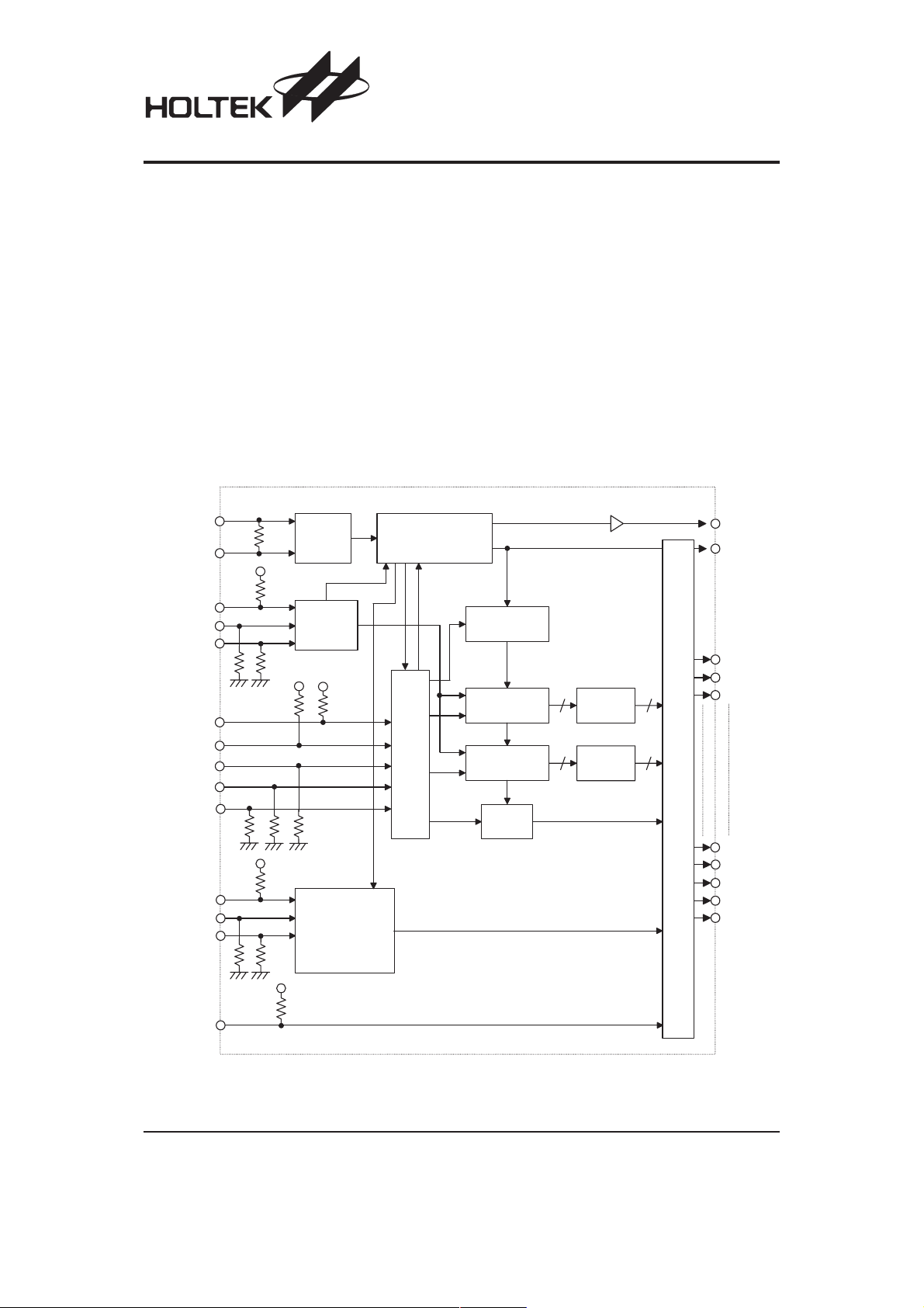
Block Diagram
HT16561
VFD Digital Clock
·
Integrated voltageregulator permitswide 4Vto 16V
operating voltage range
·
Four level contrast control function
·
44-pin QFP package
clude a choice of adjustment modes, including single
push increment or 2Hz fast forward functions. Additional
features are provided in the form of Zero adjustment and
four levels of contrast control.
-
-
O S C O
O S C I
T E S T 3
T E S T 2
T E S T 1
A / C
C O N T 2
C O N T 1
D I M
C M O S
O s c i l l a t o r
V
D D
T e s t
A d j u s t m e n t
V
D D
V
D D
S E
Z A
M S
H S
V
D D
C o n t r a s t
A d j u s t m e n t
F r e q u e n c y D i v i d e r s
T i m e A d j u s t m e n t
1 H z
S e c o n d C o u n t e r
( 1 / 6 0 )
M i n u t e C o u n t e r
( 1 / 6 0 )
H o u r C o u n t e r
( 1 / 1 2 )
A M / P M
D e c o d e r
S e g m e n t
D r i v e r [ P C H O p e n D r a i n ]
D e c o d e r
S e g m e n t
6 4 H z
1 H z
a 1
b 1
c 1
g 3
b 4
c 4
A M
P M
V
D D
T E S T 4
Rev. 1.00 1 February 7, 2007
Page 2
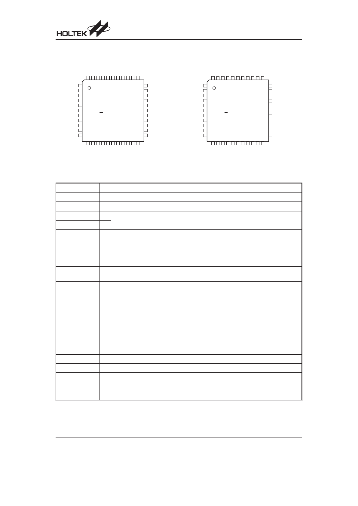
HT16561
Pin Assignment
T E S T 4
T E S T 1
P M
Z A
c 4
g 3
1
2
e 3
d 3
3
c 3
4
5
g 2
e 2
6
7
c 2
g 1
8
e 1
9
d 1
1 0
c 1
1 1
1 2 1 3 1 4 1 5 1 6 1 7 1 8 1 9 2 0 2 1 2 2
V D D
S E
D I M
6 4 H z
N C
H T 1 6 5 6 1
4 4 Q F P - A
N C
C O N T 1
T E S T 2
T E S T 3
M S
A M
H S
3 43 53 63 73 83 94 04 14 24 34 4
b 4
3 3
3 2
f 3
a 3
3 1
b 3
3 0
1 H z
2 9
f 2
2 8
a 2 , d 2
2 7
b 2
2 6
f 1
2 5
a 1
2 4
b 1
2 3
C O N T 2
A / C
O S C O
O S C I
V S S
c 4
P M
Z A
T E S T 1
T E S T 4
N C
T E S T 3
T E S T 2
M S
H S
A M
d 3
e 3
g 3
c 3
1
2
3
4
5
6
7
8
9
1 0
1 1
1 2 1 3 1 4 1 5 1 6 1 7 1 8 1 9 2 0 2 1 2 2
b 3
a 3
f 3
b 4
Pin Description
Pin Name I/O Description
VDD O High voltage power supply pin.
VSS
DIM I
CONT1 I
CONT2 I
A/C I
ZA I
HS I
MS I
SE I
OSCO O
OSCI I
TEST1, TEST2 I IC test pin - should be left open or kept at a low level
TEST3, TEST4 I IC test pin - should be left open or kept at a high level
64Hz O 64Hz signal output pin for oscillation frequency adjustment
a1, a3 ~ b2, b4, c4
1Hz
Ground pin.
¾
Illumination level control pins.
Internally connected to pull-down resistors.
Illumination level control pins.
Internally connected to pull-up resistors.
When the A/C pin is low, the internal circuits are reset.
The reset pulse width should be more than 2ms.
Internally connected to a pull-up resistor.
Zero adjustment pin.
Internally connected to a pull-down resistor.
Hour adjustment pin.
Internally connected to a pull-down resistor.
Minute adjustment pin.
Internally connected to a pull-down resistor.
Set enable pin.
Internally connected to a pull-up resistor.
Crystal oscillator pin
O Segment output pins for VFDAM, PM
e 2
g 2
H T 1 6 5 6 1 B
4 4 Q F P - B
f 2
1 H z
d 1
e 1
g 1
c 2
a 2 , d 2
c 1
3 43 53 63 73 83 94 04 14 24 34 4
6 4 H z
3 3
3 2
D I M
S E
3 1
V D D
3 0
C O N T 1
2 9
N C
2 8
C O N T 2
2 7
V S S
2 6
O S C I
2 5
O S C O
2 4
A / C
2 3
b 1
a 1
f 1
b 2
Rev. 1.00 2 February 7, 2007
Page 3
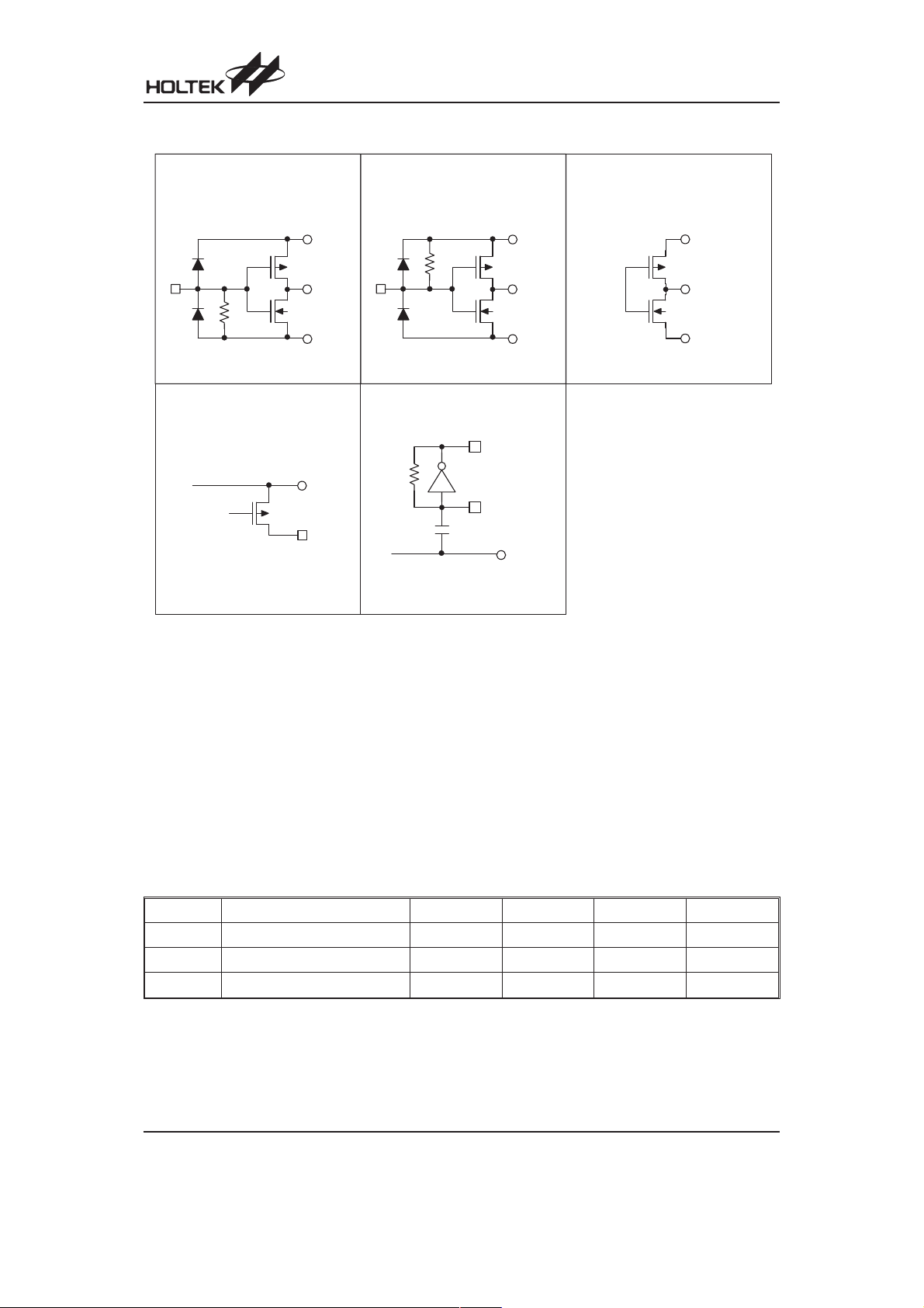
Approximate Internal Connections
HT16561
Z A , M S , H S , D I M , C O N T 1 ,
T E S T 1 , T E S T 2
a 1 , a 3 ~ g 1 , g 3 ; a 2 , d 2 ~ g 2 ;
A M , P M
V D D
V S S
V D D
A / C , S E , C O N T 2 , T E S T 3 , T E S T 4
V D D
V S S
O S C I , O S C O
O S C O
( O s c i l l a t o r O u t p u t )
O S C I
( O s c i l l a t o r I n p u t )
V S S
6 4 H z
V D D
V S S
Absolute Maximum Ratings
Logic Supply Voltage .................VSS-0.3V to VSS+6.5V
High Input Voltage .....................V
Driver Output Voltage..........................V
-0.3V to VCC+0.3V
SS
-0.3V to V
SS
DD
Driver Output Current (Grid Driver) ......-7mA to +20mA
Driver Supply Voltage .................V
High Output Voltage ..................V
Driver Output Current (Segment Driver) -10mA to +2mA
Storage Temperature..........................-55°C to +150°C
Operating Temperature.........................-40°Cto+85°C
Note: These are stress ratings only. Stresses exceeding the range specified under ²Absolute Maximum Ratings² may
cause substantial damage to the device. Functional operation of this device at other conditions beyond those listed
in the specification is not implied and prolonged exposure to extreme conditions may affect device reliability.
-0.3V to VSS+20V
SS
-0.3V to VCC+0.3V
SS
Recommended Operating Conditions
Symbol Parameter Min. Typ. Max. Unit
V
f
OSC
t
OP
DD
Power Supply Voltage 4
Oscillation Frequency
Operating Temperature
-40 ¾
¾
¾
4.194304
16 V
¾
MHz
85
°C
Rev. 1.00 3 February 7, 2007
Page 4

HT16561
D.C. Characteristics
Symbol Parameter
V
V
I
I
I
I
V
V
I
I
I
I
I
I
I
IH
IL
IH
IL1
IL2
IL3
OL
OH
OH1
OL1
OH2
OL2
OH3
OL3
DD
High Input Voltage 6V
Low Input Voltage 6V
Hi-level Input Current 6V
Low-level Input Current 6V
Low-level Output current 6V
Hi-level Output current 6V
Output Current 6V
Output Current 6V
Output Current 6V
Output Current 6V
Output Current 6V
Output Current 6V
Dynamic Current Consumption 6V
Test Conditions
V
DD
Conditions
¾
¾¾¾
for TEST1,TEST2,
V
I=VDD
ZA, MS, HS, DIM, CONT1
for TEST3, TEST4
V
I=Vss
VI=Vssfor A/C
VI=Vssfor SE, CONT2
for all pin
I
OL=VSS
I
V
for 64Hz pin
OH=VSS
=4.0V for 1Hz, a2, d2,
OH
a4, d4, e4, g4
=0V for 1Hz, a2, d2,
V
OL
a4, d4, e4, g4
=4.0V, Other segment
V
OH
output pins except above
OL=VSS
, Other segment
V
output pins except above
=5.5V for 64Hz pin
V
OH
=0.5V for 64Hz pin
V
OL
f
=4.194304MHz,
OSC
No load, C
C
OUT
C
=70W±5%
I
IN
=33pF±5%,
=39pF±5%,
VDD=6.0V, VSS=0V, Ta=-40°C~85°C
Min. Typ. Max. Unit
4.3
¾¾
V
1.0 V
30
¾
150
mA
-120 ¾-800 mA
-3 ¾-12 mA
-30 ¾-150 mA
5.9
¾¾
¾¾
0.1 V
V
¾¾-2000 mA
1
¾¾mA
¾¾-1000 mA
1
¾¾mA
¾¾-100 mA
100
¾¾
¾¾mA
2mA
Characteristics Curves
VDDvs IDDCharacteristics Curve
D D
D D
I
v s V
I
( m A )
D D
2 . 5
2 . 0
1 . 5
1 . 0
0 . 5
0
2 4 6 8 1 0 1 2 1 4 1 6 1 8
C h a r a c t e r i s t i c s C u r v e
Rev. 1.00 4 February 7, 2007
V
D D
Ta=25°C
( V )
Page 5

Functional Description
VFD Display Driving
The device can directly drive VFD clock panels dynami
cally. The clock will be displayed in a 12-hour format with
the hours ranging from 1 to 12 and and minutes from 00
to 59. If the most significant numeral is zero then the dis
play will be extinguished.
·
Segment connections
A 7-segment display is shown below showing the illu
mination pattern for each numeral.
As the device is designed for clock applications, four
7-segment displays are required to display the correct
time output. The connections for the segments are
shown below, however it should be noted that the
fourth segment only requires two of its segments to be
driven.
A M
P M
b 4
c 4
d i g i t 4 d i g i t 3
A
F
B
G
7 - S e g m e n t s
E
C
D
a 3
f 3
e 3
1 H z
b 3
g 3
c 3
d 3
1 H z
a 2
f 2
g 2
e 2
d 2
d i g i t 2 d i g i t 1
a 1
f 1
b 2
c 2
b 1
g 1
e 1
c 1
d 1
Other Pin Functions
The external reset pin A/C is used to reset the internal
circuit of the device. When this pin is pulled low the de
vice will be reset, when the pin is allowed to go high, via
its internal pull-high resistor, then the display will indi
-
cate a ²1:00² output.
In the open status, the SE pin is held to ²high² level by a
pull-high resistor, enabling the inputs from MS, HS and
ZA pins. These inputs become invalid by setting this pin
to a ²low² level externally.
The 64Hz pin allows monitoring of the system frequency
to allow frequency adjustments to be executed. As the
name suggests, this output pin will continuously output
a frequency of 64Hz.
In the open status, the TEST1 and TEST2 pins are kept
at a ²0² level by pull-down resistors.
In the open status, the TEST3 and TEST4 pins are kept
at a ²1² level by pull-up resistors.
The Test pinfunction isas shownin the following table.
HT16561
-
-
TEST select function 1
Switch Pin Name
TEST1 TEST2 TEST3
0
(or Open)0(or Open)1(or Open)
F(Pulse)
1
1
F(Pulse)
F(Pulse)
1
F(Pulse)
F(Pulse)
1 0 Input pulses to the 64Hz system of the circuit.
0
(or Open)
1
(or Open)
1
(or Open)
0 Input pulses to the 64Hz system of the circuit.
0
Normal function
Input pulses to the 16.384KHz system of the circuit.
Input pulses to the 16.384KHz system of the circuit.
Input pulses for the minute and hour counters, which advances 1 count
with 1 pulse. No carry functions for hour and minute counters.
Operating mode
TEST select function 2
Switch Pin Name
TEST3 DIM CONT1 CONT2
0
F(Pulse)
**
The pulse widths of the all segment outputs are controlled
by the pulse width of the DIM signal
Operating mode
0 0 * * Sets all segment outputs to high impedance
Note: ²*² Indicates that the input level can be ²0² and ²1²
Rev. 1.00 5 February 7, 2007
Page 6

HT16561
Three illumination level set pins, DIM, CONT1 and CONT2 are provided to give control over the display brightness
level, as shown in the following table.
Switch Pin Name
DIM CONT1 CONT2
0
(or Open)
1
1
11
* * 100% duty display
0
(or Open)1(or Open)
0
(or Open)
0 12.5% (1/8) duty display at 4096Hz
1
(or Open)
25% (1/4) duty display at 4096Hz
6.25% (1/16) duty display at 4096Hz
Note: ²1² high level, ²0² low level, ²*² don¢t care
Device Functions
·
Reset
Although the device is provided with an external reset
pin A/C, the device will in fact reset itself when power
is applied, eliminating the need for external reset com
ponents. The usual provision of an external capacitor
is not required as an internal reset capacitor is inte
grated within the device.
·
Chatter removal
The device contains circuits which are connected to
input pins HS, MS and ZA to remove chatter of less
than 31.25ms.
·
Oscillator
The basic time base frequency for this device is determined by an external 4.194304MHz crystal. When an
external crystal along with two small external capacitors are connected to the two oscillator pins, the internal oscillator circuit will ensure generation of the
correct time base signals. The oscillation frequency,
although determined by the external crystal fre
quency, will also be influenced by the external capaci
tors, the crystal inherent capacitance and the residual
capacitance of the external PCB tracks. To ensure ac
curate frequency generation, the crystal specification
should be taken into account and care taken to place
the external capacitors and crystal as close to the de
vice as possible.
Time Adjustment Operation
·
Hour/minute adjustment
Both the minutes and hour displays can be adjusted
separately or both together in a fast forward format.
The hour set pin, HS, and the minutes set pin, MS, are
used to make these adjustments. Both of these pins
are connected to internal pull-low resistors. Each time
one of these lines is pulled high, the respective hour or
minute value will increment by one, also if the line is
continuously held high then the respective value will
increment automatically at a rate of 2Hz. Both values
will increment together if both lines are pulled high si
multaneously. Note that no carry functions will be im
plemented when either the hour or minute value
overflows.
·
-
-
-
-
-
-
-
-
Operating mode
Zero adjustment
A zero adjust function is also included within the de
vice and is controlled by the ZA pin. This pin is con
nected to an internal pull low resistor. Pulling this line
high will reset both the internal minutes and seconds
value, however the way in which the display is reset
depends upon the present value of display. If the min
ute value is presently less than 30 the only the second
and minute values will be reset to zero and the hour
value remain unchanged. However if the minute value
is presently at a value of 30 or higher then when the
zero adjustment function is executed, a carry will be
implemented and the hour value will be increment by
one. The following table illustrates a few examples of
this operation.
Zero Adjust Examples
Present Time After Zero Adjust
Hr. Min. Sec. Hr. Min. Sec.
1 30 00 2 00 00
2 00 00 2 00 00
2 29 59 2 00 00
2 30 00 3 00 00
2 59 59 3 00 00
3 29 59 3 00 00
-
-
-
Rev. 1.00 6 February 7, 2007
Page 7

Application Circuits
V
D D
T E S T 1
T E S T 2
H S
M S
Z A
D I M
C O N T 1
T E S T 3
T E S T 4
S E
A / C
C O N T 2
T E S T 1
T E S T 2
H S
M S
Z A
D I M
C O N T 1
T E S T 3
T E S T 4
S E
A / C
C O N T 2
V D D
V S S
HT16561
F +
1 H z
a 1
b 1
c 1
d 1
e 1
f 1
g 1
a 2 , d 2
b 2
c 2
e 2
f 2
g 2
a 3
b 3
c 3
d 3
e 3
f 3
g 3
b 4
c 4
A M
P M
C 1
J 1
E fV
F -
S t a t i c T y p e
C l o c k V F D
C C
1 H z
a 1
b 1
c 1
d 1
e 1
f 1
g 1
a 2 , d 2
b 2
c 2
e 2
f 2
g 2
a 3
b 3
c 3
d 3
e 3
f 3
g 3
b 4
c 4
A M
P M
O S C O
O S C I
6 4 H z
Y 1
4 . 1 9 4 3 0 4 M H z
C 2
1
C O N 1
Note: Capacitors C1 and C2 can adjust the frequency accuracy
Rev. 1.00 7 February 7, 2007
Page 8

Package Information
44-pin QFP (10´10) Outline Dimensions
HT16561
C
D
2 3
1 11
Dimensions in mm
Symbol
3 3
3 4
A
B
4 4
Min. Nom. Max.
A13
B 9.9
C13
D 9.9
E
F
¾
¾
G 1.9
H
I
¾¾
¾
J 0.73
K 0.1
2 2
F
E
1 2
¾
¾
¾
¾
0.8
0.3
¾
0.1
¾
¾
H
G
K
a 0°¾7°
I
=
J
13.4
10.1
13.4
10.1
¾
¾
2.2
2.7
¾
0.93
0.2
Rev. 1.00 8 February 7, 2007
Page 9

Preliminary
Holtek Semiconductor Inc. (Headquarters)
No.3, Creation Rd. II, Science Park, Hsinchu, Taiwan
Tel: 886-3-563-1999
Fax: 886-3-563-1189
http://www.holtek.com.tw
Holtek Semiconductor Inc. (Taipei Sales Office)
4F-2, No. 3-2, YuanQu St., Nankang Software Park, Taipei 115, Taiwan
Tel: 886-2-2655-7070
Fax: 886-2-2655-7373
Fax: 886-2-2655-7383 (International sales hotline)
HT16561
Holtek Semiconductor Inc. (Shanghai Sales Office)
7th Floor, Building 2, No.889, Yi Shan Rd., Shanghai, China 200233
Tel: 86-21-6485-5560
Fax: 86-21-6485-0313
http://www.holtek.com.cn
Holtek Semiconductor Inc. (Shenzhen Sales Office)
5/F, Unit A, Productivity Building, Cross of Science M 3rd Road and Gaoxin M 2nd Road, Science Park, Nanshan District,
Shenzhen, China 518057
Tel: 86-755-8616-9908, 86-755-8616-9308
Fax: 86-755-8616-9722
Holtek Semiconductor Inc. (Beijing Sales Office)
Suite 1721, Jinyu Tower, A129 West Xuan Wu Men Street, Xicheng District, Beijing, China 100031
Tel: 86-10-6641-0030, 86-10-6641-7751, 86-10-6641-7752
Fax: 86-10-6641-0125
Holtek Semiconductor Inc. (Chengdu Sales Office)
709, Building 3, Champagne Plaza, No.97 Dongda Street, Chengdu, Sichuan, China 610016
Tel: 86-28-6653-6590
Fax: 86-28-6653-6591
Holtek Semiconductor (USA), Inc. (North America Sales Office)
46729 Fremont Blvd., Fremont, CA 94538
Tel: 1-510-252-9880
Fax: 1-510-252-9885
http://www.holtek.com
Copyright Ó 2007 by HOLTEK SEMICONDUCTOR INC.
The information appearing in this Data Sheet is believed to be accurate at the time of publication. However, Holtek as
sumes no responsibility arising from the use of the specifications described. The applications mentioned herein are used
solely for the purpose of illustration and Holtek makes no warranty or representation that such applications will be suitable
without further modification, nor recommends the use of its products for application that may present a risk to human life
due to malfunction or otherwise. Holtek¢s products are not authorized for use as critical components in life support devices
or systems. Holtek reserves the right to alter its products without prior notification. For the most up-to-date information,
please visit our web site at http://www.holtek.com.tw.
-
Rev. 1.00 9 February 7, 2007
 Loading...