

Page 1
Dot Character VFD Controller & Driver
Features
·
Logic voltage: 2.7V~5.5V
·
High voltage: 60V (max.)
·
Provides a driving segment for cursor display
(48 units)
·
Alphanumeric and symbolic display through built-in
ROM
·
80´8-bit display RAM
·
On chip ROM (5´8 dot), in total 248 characters,
plus 8 user-defined characters
·
Customized ROM acceptable
Applications
·
Consumer products panel function control
·
Industrial measuring instrument panel function
control
General Description
The HT16514 is a Vacuum Fluorescent Display, VFD
controller/driver with dot matrix VFD display. It consists
of 80 segment output lines and 24 grid output lines. It
can display up to 16C´2L, 20C´2L, 24C´2L.
HT16514
·
Display contents:
-
16 columns by 2 (1) rows + 32 (16) cursors
-
20 columns by 2 (1) rows + 40 (20) cursors
-
24 columns by 2 (1) rows + 48 (24) cursors
·
Supports display output (80-segment & 24-grid)
·
Parallel data input/output (switchable 4 bit or 8 bit) or
serial data input/output
·
Built-in oscillation circuit
·
144-pin LQFP package
·
Other similar application panel function control
The HT16514 has a character generator ROM which
stores up to 248´5´8 dot characters.
The HT16514 has serial/parallel interface. This VFD
controller/driver is ideal as an MCU peripheral device.
Ordering Information
Part Number Package Information
HT16514-001
HT16514-002
144-pin plastic LQFP (Fine pitch) (20´20), standard ROM (ROM code: 001)
144-pin plastic LQFP (Fine pitch) (20´20), standard ROM (ROM code: 002)
Rev. 1.00 1 October 4, 2006
Page 2
Block Diagram
T E S T O
T E S T I
R L 2
R L 1
D L S
D S 1
D S 0
M P U
I M
C S
R S , S T
R , W ( W R )
E ( R D ) , S C K
S I , S O
D B 0 ~ D B 3
D B 4 ~ D B 7
R E S E T
O S C I
O S C O
X O U T
4
4
8
I / O
I n t e r f a c e
8 8 7
R E S E T
C i r c u i t
O S C
D a t a R e g i s t e r
I n s t r u c t i o n
R e g i s t e r ( I R )
( D R )
7
I n s t r u c t i o n
D e c o r d e r
C G R A M
( 8 x 5 x 8 B i t s )
8
7 7
5
8
A d d r e s s
C o u n t e r
P a r a l l e l t o S e r i a l
D a t a C o n v e r t e r
5
C G R O M
( 2 4 8 x 5 x 8 B i t s )
8
8
D D R A M
( 8 0 x 8 B i t s )
7
T i m i n g
G e n e r a t o r
4
C r u s o r B l i n k C i r c u i t
7
2 4
HT16514
8 0 - B i t O u t p u t
L a t c h & R e g i s t e r
8 0
S e g m e n t
D r i v e r
G r i d D r i v e r
2 4
2 4 - B i t S h i f t
R e g i s t e r
S 1
S 8 0
G 1
G 2 4
Pin Assignment
N C
S 7 1
S 7 2
S 7 3
S 7 4
S 7 5
S 7 6
S 7 7
S 7 8
S 7 9
S 8 0
G 2 4
G 2 3
G 2 2
G 2 1
G 2 0
G 1 9
G 1 8
G 1 7
G 1 6
G 1 5
G 1 4
G 1 3
G 1 2
G 1 1
G 1 0
G 9
G 8
G 7
G 6
G 5
G 4
G 3
G 2
G 1
N C
V D D L G N D V H
S 6 7
S 6 8
S 6 9
S 7 0
1 0 8
1 0 9
1 4 4
1
X O U T
V D D
P G N D
V H
S 4 6
S 4 7
M P U
I M
S D O , S L K , C L , L E
S 4 1
S 4 2
S 4 3
S 4 4
S 4 5
L E
C L
R L 2
R L 1
C S
S 3 5
S 3 6
S 3 7
S 3 8
S 3 9
S 4 0
7 3
7 2
N C
S 3 4
S 3 3
S 3 2
S 3 1
S 3 0
S 2 9
S 2 8
S 2 7
S 2 6
S 2 5
S 2 4
S 2 3
S 2 2
S 2 1
S 2 0
S 1 9
S 1 8
S 1 7
S 1 6
S 1 5
S 1 4
S 1 3
S 1 2
S 1 1
S 1 0
S 9
S 8
S 7
S 6
S 5
S 4
S 3
S 2
S 1
N C
3 7
3 6
C L K
S D O
V H
P G N D
L G N D
T E S T O
P G N D
S 4 8
S 4 9
S 5 0
S 5 1
S 5 2
S 5 3
S 5 4
S 5 5
S 5 6
S 5 7
S 5 8
S 5 9
S 6 0
S 6 1
S 6 2
S 6 3
S 6 4
S 6 5
S 6 6
H T 1 6 5 1 4
1 4 4 L Q F P - A
R E S E T
O S C I
O S C O
D S 0
D S 1
D L S
T E S T I
R , W ( W R )
R S , S T
E ( R D ) , S C K
D B 2
D B 1
D B 0
S I , S O
D B 7
D B 6
D B 5
D B 4
D B 3
Rev. 1.00 2 October 4, 2006
Page 3
HT16514
Pin Description
Pin Name I/O Description
Logic System (Microprocessor Interface)
When parallel mode is selected, this pin is utilized to select the register, either Instruction Reg
ister or Data Register.
RS, ST
E (RD
), SCK I
CS
OSCI
OSCO
XOUT O Oscillator signal output pin
R,W(WR
SI, SO I/O
DB0~DB7 I/O
RESET
DS0, DS1 I
IM I
MPU I
DLS I
RL1, RL2 I Set segment outputs pin assignment. The selection table is listed as Table 1-2 & Table 1-7
TESTI I
TESTO O For IC testing only, leave this pin open.
Logic System ( To External Extension Driver)
SDO O Serial data output for extension digit driver.
SLK O
)I
0: IR (Instruction Register)
I
1: DR (Data Register)
When serial mode is selected, this pin performs strobe input. Data can be set as input when
this signal goes 0.
During the next rising edge of this signal, command processing is performed.
When M68parallel mode is selected (E), this pin is write enable. Writes data at the falling edge.
When i80 parallel mode is selected (RD), this pin is read enable. Whenthis pin is ²Low², data is
output to the data Bus.
When Serialmode is selected, this pin is shift clock input,data will be written at the rising edge.
I
When this pin is ²Low², the device is active.
I
Connected to an external resistor to generate an oscillation frequency.
O
When M68 parallel mode is selected (R, W), this pin is data mode select pin
(0: write, 1: read).
When i80 parallel mode is selected (WR
rising edge signal.
When serial mode is selected, connect this pin to ²Hi² or ²Low². Read or Write is chosen by in
struction.
When serial mode is selected, this pin is used as I/O pin.
When parallel mode is selected, this pin needs to be connected to ²Hi² or ²Low².
When parallel mode is selected, these pins are used as I/O pins.
Data are stored sequentially, the first bit which is sent to the HT16514 is MSB.
If 4 bits mode is selected, only DB4~DB7 are used.
Initialize all the internal register and commands.
I
All segments and digits are fixed PGND.
Set the duty ratio. Duty ratio will determine the number of grid.
The relationship between duty ratio and these pins is shown in Table 1-1.
Select interface mode (parallel mode or serial mode)
0: Serial mode
1: Parallel mode
In parallel mode, instruction will determine the length of word.
Select interface mode (i80 type CPU mode or M68 type CPU mode)
0: i80 type CPU mode
1: M68 type CPU mode
Select number of display line when power ON reset or resetting.
0: Select 1 line (N=0), ²N² is display line select flag in Function set command.
1: Select 2 line (N=1)
0 or open: Normal operation mode
1: Test mode
Shift clock pulse for extension digit driver.
Active during rising edge
), this pin is a write enable pin. Data will be written at
-
-
Rev. 1.00 3 October 4, 2006
Page 4
Pin Name I/O Description
Clear signal for extension digit driver, active low.
CL
LE O Latch enable signal for extension digit driver.
Output Pins
G1~G24 O High-voltage output, grid output pins.
S1~S80 O High-voltage output, segment output pins.
Power System
VDD
LGND
VH
PGND
Table 1-1. Duty Ratio Setting
Note: * When setting to 1/40 duty mode, use the external extension grid driver.
The digit data stored in the latch register of the extension driver are output when this signal is
O
²Hi², if this signal is ²Low², extension driver outputs are ²Low².
Pins for logic circuit
¾
LGND is ground pin for logic circuit
¾
Power supply pins for VFD driver circuit
¾
PGND is ground pin for VFD driver circuit
¾
DS0 DS1 Duty Ratio
0 0 1/16 (# of grid = 16)
0 1 1/24 (# of grid = 24)
1 0 1/20 (# of grid = 20)
1 1 1/40 (# of grid = 40)*
HT16514
Table 1-2. Segment Setting: 2 Line Display (N=1)
RL1 RL2 Table No.
0 0 Table 1-3
0 1 Table 1-4
1 0 Table 1-5
1 1 Table 1-6
Rev. 1.00 4 October 4, 2006
Page 5

Table 1-3. The Number Of Segment Pins 1
No. Name No. Name No. Name No. Name
1 VH 37 NC 73 S35 109 NC
2 PGND 38 S1 74 S36 110 S71
3 VDD 39 S2 75 S37 111 S72
4 XOUT 40 S3 76 S38 112 S73
5 OSCO 41 S4 77 S39 113 S74
6 OSCI 42 S5 78 S40 114 S75
7 RESET
8 TESTI 44 S7 80 S42 116 S77
9 DLS 45 S8 81 S43 117 S78
10 DS1 46 S9 82 S44 118 S79
11 DS0 47 S10 83 S45 119 S80
12 R, W (WR
13 RS, ST
14 E (RD
15 SI, SO 51 S14 87 S49 123 G21
16 DB0 52 S15 88 S50 124 G20
17 DB1 53 S16 89 S51 125 G19
18 DB2 54 S17 90 S52 126 G18
19 DB3 55 S18 91 S53 127 G17
20 DB4 56 S19 92 S54 128 G16
21 DB5 57 S20 93 S55 129 G15
22 DB6 58 S21 94 S56 130 G14
23 DB7 59 S22 95 S57 131 G13
24 IM 60 S23 96 S58 132 G12
25 MPU 61 S24 97 S59 133 G11
26 CS
27 RL1 63 S26 99 S61 135 G9
28 RL2 64 S27 100 S62 136 G8
29 CL
30 LE 66 S29 102 S64 138 G6
31 SDO 67 S30 103 S65 139 G5
32 SLK 68 S31 104 S66 140 G4
33 TESTO 69 S32 105 S67 141 G3
34 LGND 70 S33 106 S68 142 G2
35 PGND 71 S34 107 S69 143 G1
36 VH 72 NC 108 S70 144 NC
), SCK 50 S13 86 S48 122 G22
43 S6 79 S41 115 S76
) 48 S11 84 S46 120 G24
49 S12 85 S47 121 G23
62 S25 98 S60 134 G10
65 S28 101 S63 137 G7
HT16514
Rev. 1.00 5 October 4, 2006
Page 6

Table 1-4. The Number Of Segment Pins 2
No. Name No. Name No. Name No. Name
1 VH 37 NC 73 S6 109 NC
2 PGND 38 S40 74 S5 110 S71
3 VDD 39 S39 75 S4 111 S72
4 XOUT 40 S38 76 S3 112 S73
5 OSC 41 S37 77 S2 113 S74
6 OSCI 42 S36 78 S1 114 S75
7 RESET
8 TESTI 44 S34 80 S42 116 S77
9 DLS 45 S33 81 S43 117 S78
10 DS1 46 S32 82 S44 118 S79
11 DS0 47 S31 83 S45 119 S80
12 R, W (WR
13 RS, ST
14 E (RD
15 SI, SO 51 S27 87 S49 123 G21
16 DB0 52 S26 88 S50 124 G20
17 DB1 53 S25 89 S51 125 G19
18 DB2 54 S24 90 S52 126 G18
19 DB3 55 S23 91 S53 127 G17
20 DB4 56 S22 92 S54 128 G16
21 DB5 57 S21 93 S55 129 G15
22 DB6 58 S20 94 S56 130 G14
23 DB7 59 S19 95 S57 131 G13
24 IM 60 S18 96 S58 132 G12
25 MPU 61 S17 97 S59 133 G11
26 CS
27 RL1 63 S15 99 S61 135 G9
28 RL2 64 S14 100 S62 136 G8
29 CL
30 LE 66 S12 102 S64 138 G6
31 SDO 67 S11 103 S65 139 G5
32 SLK 68 S10 104 S66 140 G4
33 TESTO 69 S9 105 S67 141 G3
34 LGND 70 S8 106 S68 142 G2
35 PGND 71 S7 107 S69 143 G1
36 VH 72 NC 108 S70 144 NC
), SCK 50 S28 86 S48 122 G22
43 S35 79 S41 115 S76
) 48 S30 84 S46 120 G24
49 S29 85 S47 121 G23
62 S16 98 S60 134 G10
65 S13 101 S63 137 G7
HT16514
Rev. 1.00 6 October 4, 2006
Page 7
Table 1-5. The Number Of Segment Pins 3
No. Name No. Name No. Name No. Name
1 VH 37 NC 73 S75 109 NC
2 PGND 38 S41 74 S76 110 S10
3 VDD 39 S42 75 S77 111 S9
4 XOUT 40 S43 76 S78 112 S8
5 OSCO 41 S44 77 S79 113 S7
6 OSCI 42 S45 78 S80 114 S6
7 RESET
8 TESTI 44 S47 80 S39 116 S4
9 DLS 45 S48 81 S38 117 S3
10 DS1 46 S49 82 S37 118 S2
11 DS0 47 S50 83 S36 119 S1
12 R, W (WR
13 RS, ST
14 E (RD
15 SI, SO 51 S54 87 S32 123 G21
16 DB0 52 S55 88 S31 124 G20
17 DB1 53 S56 89 S30 125 G19
18 DB2 54 S57 90 S29 126 G18
19 DB3 55 S58 91 S28 127 G17
20 DB4 56 S59 92 S27 128 G16
21 DB5 57 S60 93 S26 129 G15
22 DB6 58 S61 94 S25 130 G14
23 DB7 59 S62 95 S24 131 G13
24 IM 60 S63 96 S23 132 G12
25 MPU 61 S64 97 S22 133 G11
26 CS
27 RL1 63 S66 99 S20 135 G9
28 RL2 64 S67 100 S19 136 G8
29 CL
30 LE 66 S69 102 S17 138 G6
31 SDO 67 S70 103 S16 139 G5
32 SLK 68 S71 104 S15 140 G4
33 TESTO 69 S72 105 S14 141 G3
34 LGND 70 S73 106 S13 142 G2
35 PGND 71 S74 107 S12 143 G1
36 VH 72 NC 108 S11 144 NC
), SCK 50 S53 86 S33 122 G22
43 S46 79 S40 115 S5
) 48 S51 84 S35 120 G24
49 S52 85 S34 121 G23
62 S65 98 S21 134 G10
65 S68 101 S18 137 G7
HT16514
Rev. 1.00 7 October 4, 2006
Page 8

Table 1-6. The Number Of Segment Pins 4
No. Name No. Name No. Name No. Name
1 VH 37 NC 73 S46 109 NC
2 PGND 38 S80 74 S45 110 S10
3 VDD 39 S79 75 S44 111 S9
4 XOUT 40 S78 76 S43 112 S8
5 OSCO 41 S77 77 S42 113 S7
6 OSCI 42 S76 78 S41 114 S6
7 RESET
8 TESTI 44 S74 80 S39 116 S4
9 DLS 45 S73 81 S38 117 S3
10 DS1 46 S72 82 S37 118 S2
11 DS0 47 S71 83 S36 119 S1
12 R, W (WR
13 RS, ST
14 E (RD
15 SI, SO 51 S67 87 S32 123 G21
16 DB0 52 S66 88 S31 124 G20
17 DB1 53 S65 89 S30 125 G19
18 DB2 54 S64 90 S29 126 G18
19 DB3 55 S63 91 S28 127 G17
20 DB4 56 S62 92 S27 128 G16
21 DB5 57 S61 93 S26 129 G15
22 DB6 58 S60 94 S25 130 G14
23 DB7 59 S59 95 S24 131 G13
24 IM 60 S58 96 S23 132 G12
25 MPU 61 S57 97 S22 133 G11
26 CS
27 RL1 63 S55 99 S20 135 G9
28 RL2 64 S54 100 S19 136 G8
29 CL
30 LE 66 S52 102 S17 138 G6
31 SDO 67 S51 103 S16 139 G5
32 SLK 68 S50 104 S15 140 G4
33 TESTO 69 S49 105 S14 141 G3
34 LGND 70 S48 106 S13 142 G2
35 PGND 71 S47 107 S12 143 G1
36 VH 72 NC 108 S11 144 NC
), SCK 50 S68 86 S33 122 G22
43 S75 79 S40 115 S5
) 48 S70 84 S35 120 G24
49 S69 85 S34 121 G23
62 S56 98 S21 134 G10
65 S53 101 S18 137 G7
HT16514
Rev. 1.00 8 October 4, 2006
Page 9
Table 1-7. Segment Setting: 1 Line Display (N=0)
RL1 RL2 Table No.
Don¢t care
Don¢t care
Table 1-8. The Number Of Segment Pins 5
No. Name No. Name No. Name No. Name
1 VH 37 NC 73 S35 109 NC
2 PGND 38 S1 74 S36 110
3 VDD 39 S2 75 S37 111
4 XOUT 40 S3 76 S38 112
5 OSCO 41 S4 77 S39 113
6 OSCI 42 S5 78 S40 114
7 RESET
8 TESTI 44 S7 80 116
9 DLS 45 S8 81 117
10 DS1 46 S9 82 118
11 DS0 47 S10 83 119
12 R, W (WR
13 RS, ST
14 E (RD
15 SI, SO 51 S14 87 123 G21
16 DB0 52 S15 88 124 G20
17 DB1 53 S16 89 125 G19
18 DB2 54 S17 90 126 G18
19 DB3 55 S18 91 127 G17
20 DB4 56 S19 92 128 G16
21 DB5 57 S20 93 129 G15
22 DB6 58 S21 94 130 G14
23 DB7 59 S22 95 131 G13
24 IM 60 S23 96 132 G12
25 MPU 61 S24 97 133 G11
26 CS
27 RL1 63 S26 99 135 G9
28 RL2 64 S27 100 136 G8
29 CL
30 LE 66 S29 102 138 G6
31 SDO 67 S30 103 139 G5
32 SLK 68 S31 104 140 G4
33 TESTO 69 S32 105 141 G3
34 LGND 70 S33 106 142 G2
35 PGND 71 S34 107 143 G1
36 VH 72 NC 108 144 NC
) 48 S11 84 120 G24
), SCK 50 S13 86 122 G22
0 Table 1-8
1 Table 1-9
43 S6 79
49 S12 85 121 G23
62 S25 98 134 G10
65 S28 101 137 G7
Don¢t use
115
HT16514
Don¢t use
Rev. 1.00 9 October 4, 2006
Page 10

Table 1-9. The Number Of Segment Pins 6
No. Name No. Name No. Name No. Name
1 VH 37 NC 73 S6 109 NC
2 PGND 38 S40 74 S5 110
3 VDD 39 S39 75 S4 111
4 XOUT 40 S38 76 S3 112
5 OSCO 41 S37 77 S2 113
6 OSCI 42 S36 78 S1 114
7 RESET
8 TESTI 44 S34 80 116
9 DLS 45 S33 81 117
10 DS1 46 S32 82 118
11 DS0 47 S31 83 119
12 R, W (WR
13 RS, ST
14 E (RD
15 SI, SO 51 S27 87 123 G21
16 DB0 52 S26 88 124 G20
17 DB1 53 S25 89 125 G19
18 DB2 54 S24 90 126 G18
19 DB3 55 S23 91 127 G17
20 DB4 56 S22 92 128 G16
21 DB5 57 S21 93 129 G15
22 DB6 58 S20 94 130 G14
23 DB7 59 S19 95 131 G13
24 IM 60 S18 96 132 G12
25 MPU 61 S17 97 133 G11
26 CS
27 RL1 63 S15 99 135 G9
28 RL2 64 S14 100 136 G8
29 CL
30 LE 66 S12 102 138 G6
31 SDO 67 S11 103 139 G5
32 SLK 68 S10 104 140 G4
33 TESTO 69 S9 105 141 G3
34 LGND 70 S8 106 142 G2
35 PGND 71 S7 107 143 G1
36 VH 72 NC 108 144 NC
), SCK 50 S28 86 122 G22
43 S35 79
) 48 S30 84 120 G24
49 S29 85 121 G23
62 S16 98 134 G10
65 S13 101 137 G7
Don¢t use
115
HT16514
Don¢t use
Rev. 1.00 10 October 4, 2006
Page 11
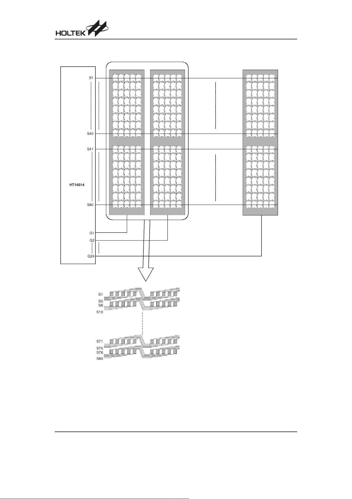
HT16514 Connect to VFD as Below Figure
HT16514
Rev. 1.00 11 October 4, 2006
Page 12
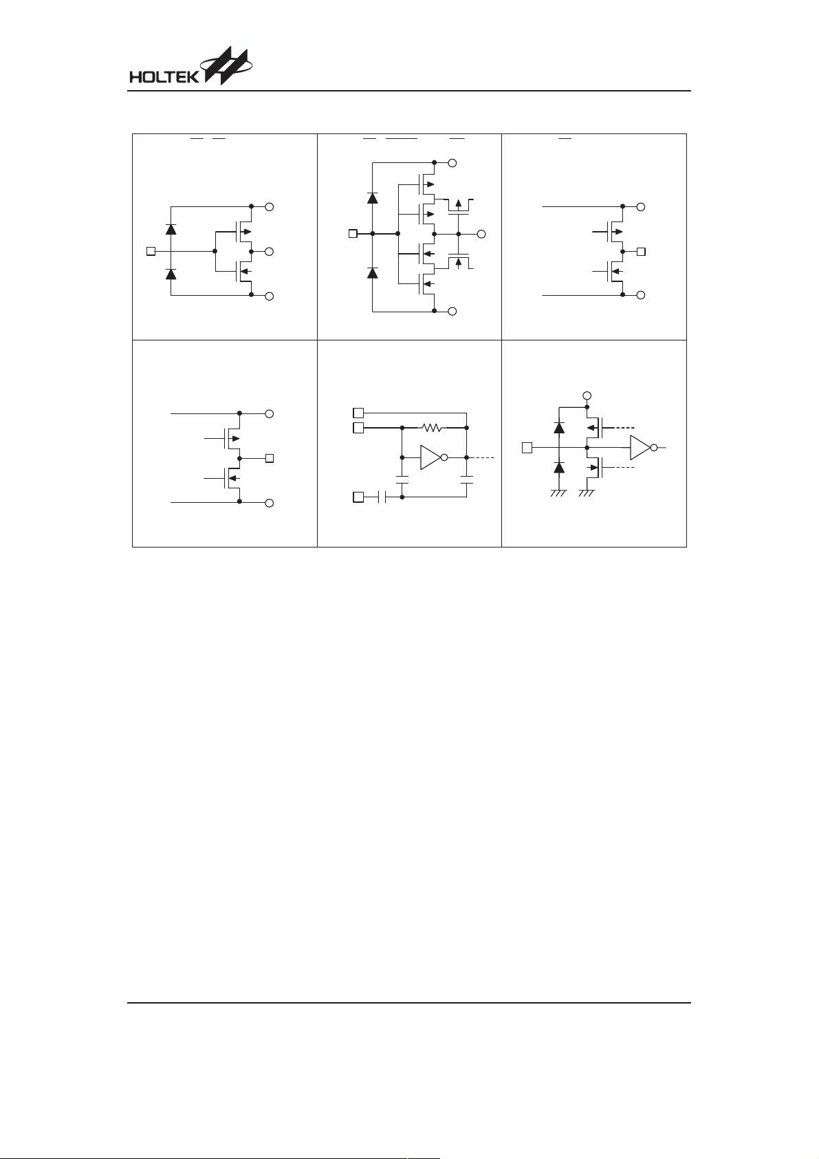
Approximate Internal Connections
HT16514
( M P U ) ( R S , S T ) ( C S ) ( D L S ) ( D S 0 ) ( D S 1 )
( I M ) ( R L 1 ) ( R L 2 ) ( T E S T I )
V
D D
L G N D
S 1 ~ S 8 0 , G 1 ~ G 2 4
V H
P G N D
S L K , E ( R D ) , R E S E T , ( R , W / W R ) S D O , S L K C L , L E , T E S T O
V
D D
L G N D
O S C O , O S C I , X O U T
X O U T
O S C O
O S C I
D 0 ~ D 7 , S I , S O
V
V
D D
L G N D
D D
Absolute Maximum Ratings
Logic Supply Voltage .................VSS-0.3V to VSS+6.0V
Input Voltage..............................V
Driver Output Voltage............................V
-0.3V to VDD+0.3V
SS
-0.3V to V
SS
Driver Output Current (Total) ...................500 (Est.) mA
Driver Supply Voltage .................V
Output Voltage...........................V
Driver Output Current .........................................±50mA
H
Storage Temperature ............................-55°Cto125°C
Operating Temperature...........................-40°Cto85°C
Note: These are stress ratings only. Stresses exceeding the range specified under ²Absolute Maximum Ratings² may
cause substantial damage to the device. Functional operation of this device at other conditions beyond those
listed in the specification is not implied and prolonged exposure to extreme conditions may affect device reliabil
ity.
-0.3V to VSS+80V
SS
-0.3V to VDD+0.3V
SS
-
Rev. 1.00 12 October 4, 2006
Page 13

HT16514
D.C. Characteristics
Symbol Parameter
V
V
I
DD
I
H
I
LOH
I
LOL
I
IH
I
P
V
V
V
V
V
V
V
V
V
V
Logic Supply Voltage
DD
VFD Supply Voltage
H
Operating Current 2.7V~5.5V No load, CPU Non-access
Operating Current 2.7V~5.5V No load
Hi-level Leakage Current 2.7V~5.5V
Hi-level Leakage Current 2.7V~5.5V
Hi-level Input Current 2.7V~5.5V
Pull-up MOS Current 2.7V~5.5V DB0~DB7, SI, SO 5 125 280
²H² Input Voltage 1 ¾
IH1
²L² Input Voltage 1 ¾
IL1
²H² Input Voltage 2 ¾
IH2
²L² Input Voltage 2 ¾
IL2
Hi-level Output Voltage 2.7V~5.5V
OH1
Low-level Output Voltage 2.7V~5.5V
OL1
OH21
Hi-level Output Voltage 2.7V~5.5V
OH22
OH2G
Low-level Output Voltage 2.7V~5.5V
OL2
VH=50V, VSS=V
Test Conditions
V
DD
Conditions
¾¾
¾¾
Logic except DB0~DB7, SI,
SO, V
IN/OUT=VDD
Logic V
IN/OUT=VSS
TEST, V
IN=VDD
Except E, SCK, RESET
W (WR
)
Except E,SCK, RESET
W (WR
)
E, SCK, RESET
E, SCK, RESET
DB0~DB7, SI,SO, SDO, SLK,
,I
LE, CL
= -0.1mA
OL1
,R,
,R,
,R,W(WR)
,R,W(WR)0
V
DB0~DB7, SI,SO, SDO, SLK,
LE, CL
,I
= 0.1mA
OL1
S1~S80, I
S1~S80, I
G1~G24, I
S1~S80, G1~G24, I
= -0.5mA
OH2
= -1mA
OH2
= -15mA
OH2
OL2
= 1mA
LGND=VPGND
=0V, Ta=-40°C~85°C
Min. Typ. Max. Unit
2.7 5 5.5 V
20
¾¾
¾¾
¾¾
¾
50 V
1000
500
1
¾¾-1 mA
5
0.7V
DD
0
0.8V
DD
-0.5
DD
0
48
46
45
¾¾
500
¾
V
¾
¾
¾
¾
¾
¾
0.3V
0.2V
V
SS
V
V
DD
DD
DD
DD
DD
+0.5
¾¾
¾¾
¾¾
5V
mA
mA
mA
mA
mA
V
V
V
V
V
V
V
V
V
A.C. Characteristics
Symbol Parameter
f
OSC
f
C
t
R1
t
R2
t
F
Oscillation Frequency 2.7V~5.5V
Oscillation Frequency 2.7V~5.5V OSCI external clock 350 560 750 kHz
Rise Time
Fall Time 2.7V~5.5V
V
DD
2.7V~5.5V
2.7V~5.5V
Test Conditions
Conditions
=56kW
R
OSC
= 50pF, S1~S80
C
L
=50pF, G1~G24
C
L
= 50pF, S1~S80,
C
L
G1~G24
VH=50V, VSS=V
Min. Typ. Max. Unit
392 560 728 kHz
LGND=VPGND
=0V, Ta=-40°C~85°C
¾¾
¾¾
¾¾
2.5
0.25
2
ms
ms
ms
Switching Timing
t
F
9 0 %
S n , G n
1 0 %
t
, t
R 1
R 2
9 0 %
1 0 %
Rev. 1.00 13 October 4, 2006
Page 14

HT16514
Timing Conditions 1 for M68-Type for Parallel Mode, Write
Symbol Parameter
t
CYCLE
PW
PW
t
AS
t
AH
t
CH
t
DS
t
DH
t
WRE
Enable Cycle Time
Enable Pulse Width High
EH
Enable Pulse Width Low
EL
((RS), (R, W), (CS)) ¾ (E)
Setup Time
((RS), (R, W)) ¾ (E)
Hold Time
(CS) ¾ (E) Hold Time
Write Data Setup Time
Write Data Hold Time
Reset Pulse Width
Test Conditions
V
DD
Conditions
4.5V~5.5V
2.7V~4.5V 1000
4.5V~5.5V
2.7V~4.5V 450
4.5V~5.5V
2.7V~4.5V 450
E®E
E
E
4.5V~5.5V
2.7V~4.5V 60
RS, R, W, CS ® E
4.5V~5.5V
2.7V~4.5V 20
E¯®RS, R, W
4.5V~5.5V
2.7V~4.5V 40
E¯®CS
4.5V~5.5V
2.7V~4.5V 195
Data ® E
4.5V~5.5V
2.7V~4.5V 10
E¯®Data
4.5V~5.5V
2.7V~4.5V 500
Ta=25°C
Min. Typ. Max. Unit
500
¾¾
¾¾
230
¾¾
¾¾
230
¾¾
¾¾
20
¾¾
¾¾
10
¾¾
¾¾
20
¾¾
¾¾
80
¾¾
¾¾
10
¾¾
¾¾
¾
500
¾¾
¾¾
ns
ns
ns
ns
ns
ns
ns
ns
ns
ns
ns
ns
ns
ns
ns
ns
ns
ns
M68-Type for Parallel Mode, Read
Symbol Parameter
t
CYCLE
PW
PW
t
AS
t
AH
t
CH
t
DD
t
DHr
Enable Cycle Time
Enable Pulse Width High
EH
Enable Pulse Width Low
EL
((RS), (R, W), (CS)) ¾ (E)
Setup Time
((RS), (R, W)) ¾ (E)
Hold Time
(CS) ¾ (E) Hold Time
Read Data Setup Time
Read Data Hold Time
Test Conditions
V
DD
Conditions
4.5V~5.5V
2.7V~4.5V 1000
4.5V~5.5V
2.7V~4.5V 450
4.5V~5.5V
2.7V~4.5V 450
E®E
E
E
4.5V~5.5V
2.7V~4.5V 60
RS, R, W, CS ® E
4.5V~5.5V
2.7V~4.5V 30
E¯®RS, R, W
4.5V~5.5V
2.7V~4.5V 40
E¯®CS
4.5V~5.5V
2.7V~4.5V
Data ® E
4.5V~5.5V
2.7V~4.5V 5
E¯®Data
Min. Typ. Max. Unit
500
230
230
20
10
20
¾¾
¾¾
5
Ta=25°C
¾¾
¾¾
¾¾
¾¾
¾¾
¾¾
¾¾
¾¾
¾¾
¾¾
¾¾
¾¾
160 ns
360 ns
¾¾
¾¾
ns
ns
ns
ns
ns
ns
ns
ns
ns
ns
ns
ns
ns
ns
Rev. 1.00 14 October 4, 2006
Page 15

Parallel Mode (M68 Input)
R S
R , W
HT16514
C S
E
D B 0
D B 7
Parallel Mode (M68 Output)
R S
R , W
C S
t
A S
P W
E H
t
D S
t
A H
P W
E L
t
D H R
V a l i d D a t a
t
C Y C E
t
A S
P W
E H
t
A H
P W
E L
E
t
D D
t
D H
D B 0
V a l i d D a t a
D B 7
t
C Y C E
Note: The input signal rising time and falling time (t
All timing is specified using 20% and 80% of V
is specified as the overlap between CS being L and E.
PW
EH
) is specified at 15ns or less.
f,tr
as the reference.
DD
Rev. 1.00 15 October 4, 2006
Page 16

HT16514
Timing Conditions 2 for i80-Type, Parallel Mode
Symbol Parameter
t
RH8
t
CH8
t
RS8
t
CYC8
t
CCLW
t
CCLR
t
CCHW
t
CCHR
t
DS8
t
DH8
t
ACC8
t
OH8
t
WRE
RS Hold Time
CS Hold Time
RS, CS Setup Time
System Cycle Time
Control ²L² Pulse Width (WR)
Control ²L² Pulse Width (RD)
Control ²H² Pulse Width (WR)
Control ²H² Pulse Width (RD)
Data Setup Time
Data Hold Time
RD Access Time
Output Disable Time
Reset Pulse Width
V
4.5V~5.5V
2.7V~4.5V 20
4.5V~5.5V
2.7V~4.5V 40
4.5V~5.5V
2.7V~4.5V 30
4.5V~5.5V
2.7V~4.5V 600
4.5V~5.5V
2.7V~4.5V 50
4.5V~5.5V
2.7V~4.5V 200
4.5V~5.5V
2.7V~4.5V 200
4.5V~5.5V
2.7V~4.5V 200
4.5V~5.5V
2.7V~4.5V 60
4.5V~5.5V
2.7V~4.5V 20
4.5V~5.5V
2.7V~4.5V
4.5V~5.5V
2.7V~4.5V 5
4.5V~5.5V
2.7V~4.5V 500
Test Conditions
DD
RS
CS
RS, CS
WR
RD
WR
RD
DB0~DB7
DB0~DB7
DB0~DB7, C
DB0~DB7, C
Conditions
¾
=100pF
L
=100pF
L
¾
Ta=25°C
Min. Typ. Max. Unit
10
¾¾
¾¾
20
¾¾
¾¾
10
¾¾
¾¾
200
¾¾
¾¾
30
¾¾
¾¾
70
¾¾
¾¾
100
¾¾
¾¾
100
¾¾
¾¾
30
¾¾
¾¾
10
¾¾
¾¾
¾¾
¾¾
5
¾¾
¾¾
500
¾¾
¾¾
70 ns
140 ns
ns
ns
ns
ns
ns
ns
ns
ns
ns
ns
ns
ns
ns
ns
ns
ns
ns
ns
ns
ns
ns
ns
ns
ns
Rev. 1.00 16 October 4, 2006
Page 17

Parallel Mode (i80)
R S
C S
W R , R D
D B 0 ~ D B 7
( W r i t e )
D B 0 ~ D B 7
( R e a d )
HT16514
t
t
t
r
C Y C 8
t
f
t
R S 8
t
, t
C C L R
C C L W
t
f
t
A C C 8
t
D S 8
R H 8
t
, t
C C H R
C C H W
t
D H 8
t
O H 8
Note: The input signal rising time and falling time (t
All timing is specified using 20% and 80% of V
t
CCLW
and t
are specified as the overlap between CS as L and WR and RD at the L level.
CCLR
Timing Conditions 3 for Serial Mode
Symbol Parameter
t
CYK
t
WHK
t
WLK
t
HSTBK
t
DS
t
DK
t
DKSTB
t
WSTB
t
WAIT
t
ODO
Shift Clock Cycle
High-level Shift Clock Pulse
Width
Low-level Shift Clock Pulse
Width
Shift Clock Hold Time
Data Setup Time
Data Hold Time
ST Hold Time
ST Pulse Width
Wait Time
Output Data Delay Time
V
DD
4.5V~5.5V
2.7V~4.5V 1000
4.5V~5.5V
2.7V~4.5V 300
4.5V~5.5V
2.7V~4.5V 300
4.5V~5.5V
2.7V~4.5V 150
4.5V~5.5V
2.7V~4.5V 150
4.5V~5.5V
2.7V~4.5V 150
4.5V~5.5V
2.7V~4.5V 750
4.5V~5.5V
2.7V~4.5V 750
4.5V~5.5V
2.7V~4.5V 1
4.5V~5.5V
2.7V~4.5V
) is specified at 15ns or less.
f,tr
as the reference.
DD
Test Conditions
Conditions
SCK
SCK
SCK
STD¯®SCK¯
Data ® SCK
SCK®Data
SCK®ST
¾
8th CLK®1st CLK¯
ST¯®Data
Ta=25°C
Min. Typ. Max. Unit
500
200
200
100
100
100
500
500
1
¾¾
¾¾
¾¾
¾¾
¾¾
¾¾
¾¾
¾¾
¾¾
¾¾
¾¾
¾¾
¾¾
¾¾
¾¾
¾¾
¾¾ms
ns
ns
ns
ns
ns
ns
ns
ns
ns
ns
ns
ns
ns
ns
ns
ns
¾¾ms
¾¾
¾¾
150 ns
300 ns
Rev. 1.00 17 October 4, 2006
Page 18

HT16514
Symbol Parameter
t
ODH
t
WRE
Output Data Hold Time
Reset Pulse Width
Serial Mode (Input)
S T
t
H S T B K
S C K
S I
Serial Mode (Output)
Test Conditions
V
DD
4.5V~5.5V
2.7V~4.5V 5
4.5V~5.5V
2.7V~4.5V 500
t
C Y K
t
W H K
t
D S
t
W L K
t
D H
Conditions
SCK®Data
¾
Min. Typ. Max. Unit
5
500
¾¾
¾¾
¾¾
¾¾
t
D K S T B
t
t
ns
ns
ns
ns
W S T B
W S T B
S T
t
H S T B K
S C K
S O
AC Measurement Point
I n p u t
O u t p u t
R e s e t
R E S E T
t
C Y K
t
W H K
t
O D O
t
W L K
t
O D H
V
I H
V
O H
t
W R E
V
I L
V
O L
t
D K S T B
Rev. 1.00 18 October 4, 2006
Page 19

HT16514
Timing Condition for interface: M68, i80 and Serial Power On Reset
Symbol Parameter
V
t
RES
t
trDD
t
OFF
D D
Resetting Time 2.7V~4.5V
VDD Rising Time 2.7V~4.5V
VDD OFF Width 2.7V~4.5V
0 . 2 V
t
t r D D
4 . 5 V
t
O F F
I n t e r n a l
V
t
R E S
R e s e t
T i m e
DD
Test Conditions
Conditions
¾
¾
¾
RESET Timing
Symbol Parameter
t
RSTD
t
OFF
t
RST
Delay Time After Reset 5V
VDDOff Time
RST/Pulse Width Low 5V
V
5V
DD
Test Conditions
Conditions
¾
¾
¾
Ta=25°C
Min. Typ. Max. Unit
100
1
1
¾¾ms
¾¾ms
¾¾
ms
Min. Typ. Max. Unit
100
1
500
¾¾ms
¾¾
¾¾
ns
ns
V C C
R S , S T B
0 . 2 V
t
O F F
Power Supply Connection Sequence
·
Connect the PGND and LGND externally to have an
equal potential voltage
·
To avoid faulty connection, turn on the driver power
supply (V
(V
DD
turning off the driver power supply (V
·
If the power connection sequence recommended by
) after turning on the logic power supply
H
). Then turn off the logic power supply (VDD) after
).
H
Holtek is not followed, there¢s a possibility that the in
ternal logic transistors may be damaged.
4 . 5 V
t
R S T D
V o l t a g e
V
H
V
D D
-
T i m e
Rev. 1.00 19 October 4, 2006
Page 20

HT16514
Functional Description
CPU Interface
HT16514 have 4 or 8-bit parallel interface or serial interface. These modes are selected by IM pin.
·
IM=²0²: Serial mode
·
IM=²1²: Parallel mode
CPU Interface Table
IM CS
0CS
1CS
Note: Keep this pin Hi or Lo.
Registers (IR, DR)
The HT16514 has two 8-bit registers, namely, an instruction register (IR) and a data register (DR). The IR register
stores instruction code such as display clear and cursor shift. It also contains address information for display data RAM
(DDRAM) and character generator RAM (CGRAM). The IR can only be written from the MPU. The DR temporarily
stores data to be written into or read from the DDRAM or CGRAM. Data written into the DR from the MPU is automati
cally written into the DDRAM or CGRAM by internal operation. The DR is also used for data storage when reading data
from the DDRAM or CGRAM. When the address information is written into the IR, data is read and then stored into the
DR from the DDRAM or CGRAM by internal operation. Data transfer between the MPU is completed when the MPU
reads the DR. After the read, data in DDRAM or CGRAM at the next address is sent to the DR for the next read from the
MPU. These two registers can be selected by the register selector (RS) signal, (Refer to CPU Interface table).
Common M68 i80
RS R, W RD
0010Write IR data during internal operation (display clear, etc.)
0101Read data to be busy flag (DB7) and address counter (DB6~DB0)
1010
1101
RS, ST E (RD), SCK R, W (WR) MPU SI, SO DB0~DB7
ST SCK Note Note SI, SO Note
RS E (RD) R,W(WR) MPU Note DB0~DB7
Registers (IR, DR) Table
WR
Write DR data (DR®DDRAM, CGRAM)
Read DR data (DDRAM, CGRAM®DR)
Register Selection
-
Busy Flag (Read BF Flag)
Busy flag data (DB7) is always output as ²0².
Address Counter (AC)
The Address counter (AC) assigns address to both DDRAM and CGRAM. When an instruction address is written into
the IR, the address information is sent from the IR to the AC.
Selection of either DDRAM or CGRAM is also determined concurrently by the instruction. After writing into (or read
from) the DDRAM or CGRAM, the AC is automatically incremented by 1 (or decremented by 1). The cursor position are
then output to DB0~DB6 when RS=0 and R, W=1 (Refer to Registers (IR, DR) Table).
Rev. 1.00 20 October 4, 2006
Page 21

HT16514
Display Data RAM (DDRAM)
The Display data RAM (DDRAM) stores display data represented in 8-bit character codes. Its extended capacity is
80´8 bits or 80 characters. The area in the DDRAM that is not used for display can be used as general data RAM. Refer
to DDRAM address table for the relationships between DDRAM address and positions on the VFD.
The
DDRAM
Example: DDRAM address ²3FH²
·
1-line display (N=0)
Display Position
DDRAM
address (ADD) is set in the address counter (AC) as hexadecimal.
DDRAM Address Table
High Order Bits Low Order Bits
AC6 AC5 AC4 AC3 AC2 AC1 AC0
Hexadecimal Hexadecimal
0111111
3F
(Digit) 123456 7980
Address 00 01 02 03 04 05 4E 4F
(Hexadecimal)
When there are fewer than 80 display characters, the display begins at the head position. For example, if using only
one HT16514, 24 characters are displayed. When display shift operation is performed, the
shown in the following table.
Example: 1-line by 24-character Display Table
Display Position
(Digit) 123456 2324
DDRAM
Address 00 01 02 03 04 05 16 17
(Hexadecimal)
For Shift Left 01 02 03 04 05 06 17 18
For Shift Right 4F 00 01 02 03 04 15 16
DDRAM
address shifts as
Rev. 1.00 21 October 4, 2006
Page 22

HT16514
·
2-line display (N=1)
Display Position
(Digit) 123456 3940
DDRAM
When the number of display character is less than 40´2 lines, the 2 lines are displayed from the head. The first line
end address and the second line start address are not consecutive.
For example, if using only one HT16514, 24 characters ´ 2 lines are displayed. When display shift operation is per
formed, the
Example: 2-line by 24-character Display Table
DDRAM
Address 00 01 02 03 04 05 26 27
(Hexadecimal) 40 41 42 43 44 45 66 67
DDRAM
Display Position
(Digit) 123456 2324
Address 00 01 02 03 04 05 16 17
(Hexadecimal) 40 41 42 43 44 45 56 57
address shifts as shown in the following table.
-
For Shift Left
For Shift Right
·
40 Characters´2 line display
The
DDRAM
00H to 27H and 40H to 67H. The
tables below show the relationship between the
as shown in the following table.
Example: 2-line by 40-character Display Table
Display Position
(Digit) 1234 232425 3940
DDRAM
Address 00 01 02 03 16 17 18 26 27
(Hexadecimal) 40 41 42 43 56 57 58 66 67
For Shift Left
For Shift Right
01 02 03 04 05 06 17 18
41 42 43 44 45 46 57 58
27 00 01 02 03 04 15 16
67 40 41 42 43 44 55 56
stores the character code of each character being displayed on the VFD. Valid
DDRAM
00 01 02 03 17 18 19 27 00
41 42 43 44 57 58 59 57 40
27 00 01 02 15 16 17 25 26
67 40 41 42 55 56 57 65 66
not used for display characters can be used as general purpose RAM. The
HT16514 Display Extension Driver Display
address and the character position on the VFD display shift
DDRAM
DDRAM
addresses are
Rev. 1.00 22 October 4, 2006
Page 23

HT16514
·
Character Generator ROM (CGROM)
¨
CGROM for generating character patterns of 5´8 dots from 8-bit character codes, generates 248 type of character
patterns.
¨
The character codes are shown on the following page.
¨
Character codes 00H to 0FH are allocated to the CGRAM
Character Code Table 1 (ROM Code: 001)
Rev. 1.00 23 October 4, 2006
Page 24

HT16514
Character Code Table 2 (ROM Code: 002)
Rev. 1.00 24 October 4, 2006
Page 25

HT16514
Character Generator RAM (CGRAM)
The CGRAM stores the pixel information (1=pixel on, 0=pixel off) for the eight user-define 5´8 characters. Valid
CGRAM addresses are 00H to 3FH. CGRAM not used to defined characters can be used as general purpose RAM.
Character codes 00H~07H (or 08H~0FH) are assigned to the user-defined characters (see section 5.0 character font
tables). The table below shows the relationship between the character codes, CGRAM addresses, and CGRAM data
for each user-defined character.
Relationship between CGRAM address and character code (DDRAM) and 5´7 (with cursor) dot character patterns
(CGRAM)
Note:
²X² means don¢t care
C h a r a c t e r C o d e ( R A M D a t a )
D 7 D 6 D 5 D 4 D 3 D 2 D 1 D 0
H i g h O r d e r B i t L o w O r d e r B i t
X
0
0
0
0
0
0
0
0
0
0
0
0
0
0
0
0
0
0
0
0
0
0
0
0
0
0
0
0
0
0
0
0
0
0
0
0
0
0
0
0
0
0
0
0
0
0
0
X
0
0
X
0
0
X
0
0
X
0
0
X
0
0
X
0
0
X
0
0
X
0
0
X
0
0
X
0
0
X
0
0
X
0
0
X
0
0
X
0
0
X
0
0
X
0
0
X
0
0
X
0
0
X
0
0
X
0
0
X
0
0
X
0
0
X
0
0
0
0
0
0
0
0
0
0
0
0
0
0
0
0
0
0
0
0
0
0
0
0
0
0
0
0
0
1
0
0
1
0
0
1
0
0
1
0
0
1
0
0
1
0
0
1
0
0
1
0
0
1
1
1
1
1
1
1
1
1
1
1
1
1
1
1
1
1
1
1
1
1
1
1
1
C G R A M A d d r e s s
A 5 A 4 A 3
H i g h O r d e r B i t
0
0
0
0
0
0
0
0
0
0
0
0
0
0
0
0
0
0
0
0
0
0
0
0
1
0
0
1
0
0
1
0
0
1
0
0
1
0
0
1
0
0
1
0
0
1
0
0
1
1
1
1
1
1
1
1
1
1
1
1
1
1
1
1
1
1
1
1
1
1
1
1
A 2 A 1 A 0
L o w O r d e r B i t
0
0
0
0
1
0
1
0
0
1
0
1
1
1
1
1
0
0
0
0
1
0
1
0
0
1
0
1
1
1
1
1
0
0
0
0
1
0
1
0
0
1
0
1
1
1
1
1
0
1
0
1
0
1
0
1
0
1
0
1
0
1
0
1
0
1
0
1
0
1
0
1
C G R A M D a t a
D 7 D 6 D 5 D 4 D 3 D 2 D 1 D 0
H i g h O r d e r B i t L o w O r d e r B i t
X
X
X
X
X
X
X
X
X
X
X
X
X
X
X
X
X
X
X
X
X
X
X
X
X
X
X
X
X
X
X
X
X
X
X
X
X
X
X
X
X
X
X
X
X
X
X
X
X
X
X
X
X
X
X
X
X
X
X
X
X
X
X
X
X
X
X
X
X
X
X
X
0
0
0
1
0
0
0
1
0
0
0
1
1
1
1
1
0
0
1
1
1
0
1
0
0
0
0
0
0
0
1
1
1
1
1
1
1
1
0
0
0
0
0
0
0
0
0
0
1
1
1
0
0
1
0
0
1
0
0
1
0
0
1
0
0
1
0
0
1
0
0
0
0
0
0
0
0
1
0
0
1
0
0
1
0
0
1
0
0
1
0
0
0
1
1
1
1
1
1
C h a r a c t e r
1
P a t t e r n ( 1 )
1
1
1
C u r s o r P o s i t i o n
0
1
0
0
C h a r a c t e r
0
P a t t e r n ( 2 )
0
0
0
C u r s o r P o s i t i o n
0
1
0
0
C h a r a c t e r
0
P a t t e r n ( 8 )
0
0
1
C u r s o r P o s i t i o n
1
Character code bits 0~2 correspond to CGRAM address bits 3~5 (3 bits: 8 types)
CGRAM address bits 0~2 designate character pattern line position. The 8th line is the cursor position and its
display is formed by a logical OR with the cursor. Maintain the 8th line data, corresponding to the cursor display
position at 0 as the cursor display. If the 8th line data is 1, 1 bit will light up the 8th line regardless of the cursor
presence.
Character pattern row position corresponds to CGRAM data bits 0~4 (bit 4 being at the left).
CGRAM character patterns are selected when character code bits 4~7 are all 0. However, since character
code bit 3 has no effect, the N display example above can be selected by either character code 00H or 08H.
1 for CGRAM data corresponds to display selection and 0 to no selection.
Timing Generation Circuit
Timing generation circuit generates timing signals for the operation of internal circuit such as DDRAM, CGRAM and
CGROM. The RAM reads the timing for display and the internal operation timing by MPU access are generated sepa
rately to avoid interfering with each other. Therefore, when writing data to DDRAM, for example, there will be no unde
sirable interference, such as flickering, in areas other than the display area.
Rev. 1.00 25 October 4, 2006
-
-
Page 26

HT16514
VFD Driver Circuit
VFD driver circuit consists of 24 grid signal drivers and 80 segment signal drivers. When the character font and number
of digits are selected by hardware (DS0, DS1) at power on, the required grid signal drivers automatically output drive
waveforms, while the other grid signal driver continue to output non-selection waveforms.
Sending serial data is latched when the display data character pattern corresponds to the last address of the display
data RAM (DDRAM).
Since serial data is latched when the display data character pattern corresponds to the starting address enters the in
ternal shift register, the HT16514 drives from the head display.
Cursor/Blink Control Circuit
Cursor/blink control circuit generates the cursor or character blinking. The cursor or the blinking will appear with the
digit located at the display data RAM (DDRAM) address set in the address counter (AC).
For example, when the address counter is 08H, the cursor position is displayed at DDRAM address 08H.
Cursor/Blink Control Table
-
1-line Display
2-line Display
Note: The cursor or blinking appears when the address counter (AC) selects the character generator RAM
(CGRAM). However, the cursor and blinking become meaningless when the cursor or blinking is displayed in
the meaningless position when AC is a CGRAM address.
Interface With CPU Mode
·
Parallel Data Transfer M68 (IM=1, MPU=1)
This IC can interface (data transfer) with the CPU in 4 or 8 bits in M68 interface.
However, the internal registers consist of 8 bits. Using the DB4 to DB7 twice must perform data transfer in 4 bits.
When using 4-bit parallel data transfer, DB0 to DB3 pins remain Hi or Low. The transfer order is initially from the
higher 4 bits (D4 to D7) then followed by the lower 4 bits (D0 to D3).
BF checks are performed before transferring the higher 4 bits. BF checks are not required before transferring the
lower 4 bits.
Rev. 1.00 26 October 4, 2006
Page 27

¨
4-bit data transfer (M68)
R S
R , W
E
HT16514
D B 7
D B 6
D B 5
D B 4
¨
8-bit data transfer (M68)
R S
R , W
E
D B 7
D B 6
I R 7
I R 6
I R 5
I R 4
I n s t r u c t i o n
I R 7 B F = " 0 " D 7
I R 6 D 6
W r i t e
I R 3
I R 2
I R 1
I R 0
I R 7
I R 6
I R 7
I R 6
I R 5
I R 4
W r i t e
I n s t r u c t i o n
I R 3
I R 2
I R 1
I R 0
I R 6
B F = " 0 "
I R 6
I R 5
I R 4
I n s t r u c t i o n
R e a d
I R 3
I R 2
I R 1
I R 0
D 7
D 6
D 5
D 4
D 3
D 2
D 1
D 0
W r i t e
D a t a
D B 0
I R 0 D 0
W r i t e
I n s t r u c t i o n
I R 0
W r i t e
I n s t r u c t i o n
I R 0
R e a d
I n s t r u c t i o n
W r i t e
D a t a
Rev. 1.00 27 October 4, 2006
Page 28

HT16514
Parallel mode for i80 (IM=1, MPU=0)
When setting ²IM=1, MPU=0², i80 is selected. In the HT16514, each time data is sent from the MPU, a type of pipeline
process between LSIs is performed through the bus holder attached to internal data bus.
There is a certain restriction in the read sequence of this display data RAM. Please be advised that data of the specified
address is not generated by the read instruction issued immediately after the address setup. This data is generated in
data read for the second time. Thus, a dummy read is required whenever the address setup or write cycle operation is
selected. This relationship is shown in the following figure.
W r i t i n g M P U
W R
D A T A
I n t e r n a l T i m i n g
B U S
H o l d e r
W r i t e
S i g n a l
R e a d i n g M P U
W R
R D
D A T A
I n t e r n a l T i m i n g
A d d r e s s
P r e s e t
N N + 1 N + 2 N + 3
L a t c h
N N + 1 N + 2 N + 3
N n n + 1
N
R e a d
S i g n a l
C o l u m n
A d d r e s s
B U S
H o l d e r
A d d r e s s S e t
# n
P r e s e t N I n c r e m e n t N + 1 N + 2
N n n + 1 n + 2
D u m m y
R e a d
D a t a R e a d
# n
D a t a R e a d
# n + 1
Rev. 1.00 28 October 4, 2006
Page 29

HT16514
Serial Mode
In the synchronous serial interface mode, instructions and data are sent between the host and the module using 8-bit
bytes. Two bytes are required per read/write cycle and are transmitted MSB first. The start byte contains 5 high bits, the
Read/Write (R/W) control bit, the Register Select (RS) control bit, and a low bit. The subsequent byte contains the in
struction/data bits. The R/W bit determines whether the cycle is a read (high) or a write (low) cycle. The RS bitis used to
identify the second byte as an instruction (low) or data (high).
This mode uses the strobe (ST
tion. In a write cycle, bits are clocked into the module on the rising edge of SCK. In a read cycle, bits in the start byte are
clocked into the module on the rising edge of SCK. After a minimum wait time, each bit in the instruction/data byte can
be read from the module after each falling edge of SCK. Each read/write cycle begins on the falling edge of ST
ends on the rising edge. To be a valid read/write cycle, the ST
D a t a W r i t e
S T
1 2 3 4 5 6 7 8 9 1 0 1 1 1 2 1 3 1 4 1 5 1 6 1 7
S C K
) control signal, Serial Clock (SCK) input, and Serial I/O (SI/SO) line to transfer informa
and
must go high at the end of the cycle.
-
-
D a t a R e a d
S I , S O
S T
S C K
R S
S I
" 1 " " 1 " " 1 " " 1 " " 1 "
S y n c h r o n o u s B i t s
S t a r t B y t e
1 2 3 4 5
" 1 " " 1 " " 1 " " 1 " " 1 "
S y n c h r o n o u s B i t s
S t a r t B y t e
R , W
6 7 8
R S
R , W
W a i t T i m e : t
" 0 "
1ms
" 0 "
D 7 D 6 D 5 D 4
I n s t r u c t i o n / D a t a
W A I T
1 2 3 4 5
B F
I R 6 I R 5 I R 4 I R 3 I R 2 I R 1 I R 0
" 0 "
D 3
R e a d D a t a
D 2 D 1 D 0
6 7 8 9
Rev. 1.00 29 October 4, 2006
Page 30

Commands
Instruction RS R, W DB7 DB6 DB5 DB4 DB3 DB2 DB1 DB0 Description
Clear display 0000000000
Cursor home 000000001x
Entry mode set 00000001I/DS
Display On/Off 0000001DCB
Cursor or display shift 000001S/CR/Lxx
Function 00001DLNxBR1BR0
CGRAM address set 0001 ACG
DDRAM address set 0 0 1 ADD
Read busy flag &
address
Write datato CGRAM
or DDRAM
Read data from
CGRAM
Note: I/D=1: Increment, I/D=0: Decrement
or DDRAM
S=1: Display shift enable, S=0: Cursor shift enable
S/C=1: Display shift, S/C=0: Cursor shift
R/L=1: Right shift, R/L=0: Left shift
DL=1: 8bit, DL=0: 4bit
BR1, BR0= (00: 100%) , (01: 75%) , (10: 50%),(11:25%)
²X²: Don¢t care
ACG: CGRAM address
ADD: DDRAM address
ACC: Address counter
DDRAM: Display Data RAM
CGRAM: Character Generator RAM
0 1 BF=0 ACC
1 0 Write data
11
ReadDRdata
Clear all display, and
sets the DDRAM ad
dress at 00H.
Sets the DDRAM ad
dress at 00H. Also re
turns the display shifted
to the original position.
The DDRAM contents
remain unchanged.
Sets the cursor direction
and specifies the display
shift. These operations
are performed during
writing/reading data.
Sets all display
ON/OFF(D), cursor
ON/OFF(C), cursor
blink of character
position (B).
Shifts display or cursor,
while keeping the
DDRAM contents.
Sets data length
(in paralleldata transfer)
and Number of line
Sets the address of the
CGRAM. After that, data
of the DDRAM is transferred.
Sets the address of the
DDRAM. After that, data
of the DDRAM is transferred.
Reads the busy flag (BF)
and the address counter.
BF is output as ²0² al
ways.
Writes data into the
CGRAM of the DDRAM.
Reads data from the
CGRAM or DDRAM.
HT16514
-
-
-
-
Rev. 1.00 30 October 4, 2006
Page 31

Clear Display
The instruction:
·
Fills all locations in the display data RAM (DDRAM) with 20H (Blank character).
·
Clears the contents of the address counter (ACC) to 00H.
·
Sets display for zero character shifts (returns to original position).
·
Sets the address counter to point to the display data RAM (DDRAM).
·
If cursor is displayed, move cursor to the left most character in the top line (upper line).
·
Sets address counter (ACC) to increment on each access to DDRAM or CGRAM.
When resetting
Cursor Home
The instruction:
·
Clears the contents of the address counter (ACC) to 00H.
·
Sets the address counter to point to the display data RAM (DDRAM).
·
Sets display for zero character shifts (returns to original position).
·
If cursor is displayed, move cursor to the left most character in the top line (upper line).
HT16514
Entry Mode
This instruction selects whether the cursor position increments or decrements after each DDRAM or CGRAM access
and determines the direction the information on the display shifts after each DDRAM write. The instruction also enables
or disables display shifts after each DDRAM write (information on the display does not shift after a DDRAM read or
CGRAM access). The DDRAM, CGRAM, and cursor position are not affected by this instruction.
I/D=0: The AC decrements after each DDRAM or CGRAM access.
If S=1, the information on the display shifts to the right by one character position after each DDRAM write.
I/D=1: The AC increments after each DDRAM or CGRAM access.
If S=1, the information on the display shifts to the left by one character position after each DDRAM write.
S=0: The display shift function is disabled.
S=1: The display shift function is enabled.
Cursor Move and Display Shift by the Entry Mode Set
I/D S After Writing DDRAM Data After Reading DDRAM Data
0 0 Cursor moves one character to the left. Cursor moves one character to the right.
1 0 Cursor moves one character to the right. Cursor moves one character to the right.
01
11
Display shifts one character to the right without cursor
movements.
Display shifts one character to the left without cursor move
ments.
Cursor moves one character to the left.
Cursor moves one character to the right.
When resetting
Rev. 1.00 31 October 4, 2006
Page 32

Display ON/OFF
HT16514
This instruction selects whether the display and cursor are on or off and selects whether or not the character at the cur
rent cursor position blinks. The DDRAM, CGRAM, and cursor position are not affected by this instruction.
·
D=0: The display is off (display blank).
·
D=1: The display is on (contents of the DDRAM is displayed).
·
C=0: The cursor is off.
·
C=1: The cursor is on (8th rows of pixels).
·
B=0: The blinking character function is disabled.
·
B=1: The blinking character function is enabled
Note: A character with all pixels on will alternate with the character displayed at the current cursor position at a 1Hz
rate with a 50% duty cycle.
When resetting
Cursor or Display Shift
This instructionshifts the display and/or moves the cursor to theleft or right, without reading or writing to the DDRAM.
²S/C² bit selects movement of the cursor or movement of both cursor and display.
·
S/C=1: Shift both cursor and display.
·
S/C=0: Shift only the cursor.
²R/L² bit selects whether moving the direction to the left or right of the display and/or cursor.
·
R/L=1: Shift one character right.
·
R/L=0: Shift one character left.
Cursor or Display Shift
S/C R/L Cursor Position Information on the Display
0 0 Decrements by one (left) No change
0 1 Increments by one (right) No change
1 0 Decrements by one (left) Shifts on character position to the left
1 1 Increments by one (right) Shifts on character position to the right
-
Function Set
This instruction sets the width of the data bus for the parallel interface modes, the number of display lines, and the lumi
nance level (brightness) of the VFD. DDRAM, CGRAM, and cursor position are not affected by this instruction.
·
DL=0: Sets the data bus width for the parallel interface modes to 4-bit (DB7~DB4).
·
DL=1: Sets the data bus width for the parallel interface modes to 8-bit (DB7~DB0).
·
N=0: Sets the number of display lines to 1 (this setting is not recommended).
·
N=1: Sets the number of display lines to 2
Rev. 1.00 32 October 4, 2006
-
Page 33

HT16514
BR1, BR0 flag is brightness control for the VFD to modulate the pulse width of the segment output as follows.
t
DSP
@200ms, t
@10ms
BLK
BR1 BR0 Brightness t
0 0 100%
0 1 75%
1 0 50%
1 1 25%
t
t
t
t
DSP
DSP
DSP
DSP
P
´1.00
´0.75
´0.50
´0.25
Note: ²n² means number of grid, T=nx (t
DSP+tBLK
)
When resetting
CGRAM Address Set
This instruction places the 6-bit CGRAM address specified by DB5~DB0 into the cursor position. Subsequent data
writes (reads) will be to (from) the CGRAM. The DDRAM and CGRAM contents are not affected by this instruction.
When resetting: Don¢t care.
Rev. 1.00 33 October 4, 2006
Page 34

HT16514
DDRAM Address Set
This instruction places the 7-bit DDRAM address specified by DB6~DB0 into the cursor position. Subsequent data
writes (reads) will be to (from) the DDRAM. The DDRAM and CGRAM contents are not affected by this instruction.
Valid DDRAM Address Ranges
Number of Character Address Range
1st line 40 00H~27H
2nd line 40 40H~67H
When resetting: Don¢t care.
Read Busy Flag and Address
This instruction reads the Busy Flag (BF)* and the value of address counter in binary ²AAAAAAA². This address coun
ter is used by the CGRAM and DDRAM addresses, its value is determined by the previous instruction. The address
counter contents are the same as for instructions ²CGRAM address set² and ²DDRAM address set².
Note: ²*² means the Busy Flag (BF) always outputs a ²0².
Write Data to the
This instruction writes the 8-bit data byte on DB7~DB0 into the DDRAM or CGRAM location addressed by the cursor
position. The most recent DDRAM or CGRAM Address Set instruction determines whether the write is to the DDRAM
or CGRAM. This instruction also increments or decrements the cursor position and shifts the display according to the
I/D and S bits set by the Entry Mode Set instruction.
Read Data from
This instruction reads the 8-bit data byte from the DDRAM or CGRAM location addressed by the cursor position on
DB7~DB0. The most recent DDRAM or CGRAM Address Set instruction determines whether the read is from the
DDRAM or CGRAM. This instruction also increments or decrements the cursor position and shifts the display accord
ing to the I/D and S bits set by the Entry Mode Setinstruction. Before sending this instruction, a DDRAM or CGRAM Ad
dress Set instruction should be executed to set the cursor position to the desired DDRAM or CGRAM address to be
read.
After reading one data, the value of the address is automatically increased or decreased by 1 according to the selection
by ²Entry mode².
Note: The Address counter is automatically increased or decreased by 1 after a data write instruction to the CGRAM
or DDRAM are executed. But at this moment the data to be pointed to by the address counter cannot be read if
a data read instruction is executed. Therefore, to read data correctly, executing an address set instruction or
cursor shift instruction (the only case of a DDRAM data read) just before reading, or reading the second data in
case of reading data continuously by executing a read data instruction.
CGRAM
CGRAM
or DDRAM
or DDRAM
-
-
-
Rev. 1.00 34 October 4, 2006
Page 35

HT16514
Power ON Reset
After a power-on reset, the module is initialize to the following conditions:
·
All DDRAM locations are set to 20H (character code for a space).
·
The cursor position is set to
·
The relationshipbetween DDRAM addresses and character positions on the VFD is set to the non-shifted position.
·
Entry Mode Set instruction bits:
DDRAM
I/D=1: The cursor position increments after each DDRAM or CGRAM access.
If S=1, the information on the display shifts to the left by one character position after each
S=0: The display shift function is disabled.
·
Display On/Off Control instruction bits:
D=0: The display is off (display blank).
C=0: The cursor is off.
B=0: The blinking character function is disabled.
·
Function Set instruction bits:
DL=1: Sets the data bus width for the parallel interface modes to 8 bits (DB7~DB0).
N=1: Number of display lines is set to 2.
BR1, BR0=0,0: Sets the luminance level to 100%.
·
interface, duty ratio selection are based on the following table.
MPU
Relationship between Status of HT16514 and Pin Selection at Power on Reset
Pin Name
TEST IM DS1 DS0
1 x x x Self test mode This is effective on aging.
0 or open 0 x x Serial interface SI, SO, SCK, ST
0 or open 1 x x Parallel interface RS, E, R, W, DB7~DB4 or DB7~DB0
0 or open x 0 0
0 or open x 0 1
0 or open x 1 0
0 or open x 1 1
address 00H
Function Remark
Duty= 1/16 (16C´1 or 2L display)
Duty= 1/20 (20C´1 or 2L display)
Duty= 1/24 (24C´1 or 2L display)
Duty= 1/40 (40C´1 or 2L display)
DDRAM
It¢s not necessary to use the extension driver.
The number of line is selected by instruction.
Extension driver should be used.
The number of line is selected by instruction.
write.
Rev. 1.00 35 October 4, 2006
Page 36

Example (8-bit Data Parallel, Data Increment Mode)
HT16514
Initialization Sequence & Data Set
Initialization Programming Example & Data Set (M68 series MPU)
RS R, W D7 D6 D5 D4 D3 D2 D1 D0 Description
Power On
Function Set
0000111x01
0001000000CGRAM address set to 00H
x x xDDDDD
10
0010000000DDRAM address set to 00H
10
0 00001100
x x xDDDDD
||||||||
x x xDDDDD
DDDDDDDD
DDDDDDDD
||||||||
DDDDDDDD
Data length: 8 bits
Display line number: 2 lines
VFD Brightness: 75%
Write data to CGRAM 64 bytes
(8 characters)
Write data to DDRAM 80 bytes
(80 characters)
Display ON/OFF
Display ON, cursor OFF, cursor blink
OFF
Rev. 1.00 36 October 4, 2006
Page 37

Application Circuits
HT16514
M C U
Note:
R S , S T
E ( R D ) , S C K
C S
R , W ( W R )
S I , S O
D S 0 , D S 1
I M
M P U
D L S
R L 1 , R L 2
R E S E T
D B 0 ~ D D B 7
=56kW for oscillator resistor
R
OSC
O S C I
G r i d E x t e r n a l E x t e n s i o n D r i v e
S D O S L K
H T 1 6 5 1 4
O S C O
R
O S C
V D D
V
D D
L G N D
L G N D V
C L
L E
V H P G N D
H
P G N D
G 2 5 ~ G 4 0
S 1 ~ S 8 0
G 1 ~ G 2 4
E
V F D
F
Rev. 1.00 37 October 4, 2006
Page 38

Package Information
144-pin LQFP (20´20) Outline Dimensions
HT16514
C
D
1 0 8
1 0 9
B
A
1 4 4
1
7 3
7 2
F
E
3 7
3 6
H
G
I
a
K
J
Symbol
A 21.9
B 19.9
C 21.9
D 19.9
E
F
G 1.35
H
I
J 0.45
K 0.1
Min. Nom. Max.
¾
¾
¾¾
¾
Dimensions in mm
¾
¾
¾
¾
0.5
0.2
¾
0.1
¾
¾
22.1
20.1
22.1
20.1
¾
¾
1.45
1.6
¾
0.75
0.2
a 0°¾7°
Rev. 1.00 38 October 4, 2006
Page 39

Holtek Semiconductor Inc. (Headquarters)
No.3, Creation Rd. II, Science Park, Hsinchu, Taiwan
Tel: 886-3-563-1999
Fax: 886-3-563-1189
http://www.holtek.com.tw
Holtek Semiconductor Inc. (Taipei Sales Office)
4F-2, No. 3-2, YuanQu St., Nankang Software Park, Taipei 115, Taiwan
Tel: 886-2-2655-7070
Fax: 886-2-2655-7373
Fax: 886-2-2655-7383 (International sales hotline)
HT16514
Holtek Semiconductor Inc. (Shanghai Sales Office)
7th Floor, Building 2, No.889, Yi Shan Rd., Shanghai, China 200233
Tel: 021-6485-5560
Fax: 021-6485-0313
http://www.holtek.com.cn
Holtek Semiconductor Inc. (Shenzhen Sales Office)
5/F, Unit A, Productivity Building, Cross of Science M 3rd Road and Gaoxin M 2nd Road, Science Park, Nanshan District,
Shenzhen, China 518057
Tel: 0755-8616-9908, 8616-9308
Fax: 0755-8616-9533
Holtek Semiconductor Inc. (Beijing Sales Office)
Suite 1721, Jinyu Tower, A129 West Xuan Wu Men Street, Xicheng District, Beijing, China 100031
Tel: 010-6641-0030, 6641-7751, 6641-7752
Fax: 010-6641-0125
Holtek Semiconductor Inc. (Chengdu Sales Office)
709, Building 3, Champagne Plaza, No.97 Dongda Street, Chengdu, Sichuan, China 610016
Tel: 028-6653-6590
Fax: 028-6653-6591
Holmate Semiconductor, Inc. (North America Sales Office)
46729 Fremont Blvd., Fremont, CA 94538
Tel: 510-252-9880
Fax: 510-252-9885
http://www.holmate.com
Copyright Ó 2006 by HOLTEK SEMICONDUCTOR INC.
The information appearing in this Data Sheet is believed to be accurate at the time of publication. However, Holtek as
sumes no responsibility arising from the use of the specifications described. The applications mentioned herein are used
solely for the purpose of illustration and Holtek makes no warranty or representation that such applications will be suitable
without further modification, nor recommends the use of its products for application that may present a risk to human life
due to malfunction or otherwise. Holtek¢s products are not authorized for use as critical components in life support devices
or systems. Holtek reserves the right to alter its products without prior notification. For the most up-to-date information,
please visit our web site at http://www.holtek.com.tw.
-
Rev. 1.00 39 October 4, 2006
 Loading...