

HS-245RH, HS-246RH, HS-248RH
Data Sheet August 1999
HS-245RH Radiation Hardened Triple
Line Transmitter
HS-246RH Radiation Hardened Triple
Line Receiver
HS-248RH Radiation Hardened Triple
Party-Line Receiver
The HS-245RH/246RH/248RH radiation hardened triple line
transmitter and triple line receivers are fabricated using the
Intersil dielectric isolation process. These parts are identical in
pinout and function to the original HD-245/246/248. They are
also die size and bond pad placement compatible with the
original parts for those customers who buy dice for hybrid
assembly.
Each transmitter-receiver combination provides a digital
interface between systems linked by 100Ω twisted pair,
shielded cable. Each device contains three circuits
fabricated within a single monolithic chip. Data rates greater
than 15MHz are possible depending on transmission line
loss characteristics and length.
The transmitter employs constant current switching which
provides high noise immunity along with high speeds, low
power dissipation, low EMI generation and the ability to
drive high capacitance loads. In addition, the transmitters
can be turned “off” allowing several transmitters to timeshare a single line.
Receiver input/output differences are shown in the table:
PART NO. INPUT OUTPUT
HS-246RH 100Ω Open Collector
HS-248RH Hi-Z 6K Pull-Up Resistors
The internal 100Ω cable termination consists of 50Ω from
each input to ground.
HS-248RH ‘‘party line’’ receivershave a Hi-Z input such that
as many as ten of these receivers can be used on a single
transmission line.
Each transmitter inputandreceiv eroutputcan be connected to
TTL and DTL systems. When used with shielded transmission
line, the transmitter-receiver system has v ery high immunity to
capacitance and magnetic noise coupling from adjacent
conductors. The system can tolerate ground differentials of
-2.0V to +20.0V (transmitter with respect to receiver).
Specifications for Rad Hard QML devices are controlled
by the Defense Supply Center in Columbus (DSCC). The
SMD numbers listed here must be used when ordering.
Detailed Electrical Specifications for these devices are
contained in SMD 5962-96722 and 5962-96723. A “hotlink” is provided on our homepage for downloading.
http://www.intersil.com/spacedefense/space.htm
File Number 3034.2
Features
• Electrically Screened to SMD # 5962-96722 and 596296723
• QML Qualified per MIL-PRF-38535 Requirements
• Radiation Hardened DI Processing
- Total Dose (γ) . . . . . . . . . . . . . . . . . . . 2 x 10
- Latchup Free
- Neutron Fluence . . . . . . . . . . . . . . . . . 5 x 10
• Replaces HD-245/246/248
• Current Mode Operation
• High Speed with 50 Foot Cable . . . . . . . . . . . . . . . 15MHz
High Speed with 1000 Foot Cable . . . . . . . . . . . . . . 2MHz
• High Noise Immunity
• Low EMI Generation
• Low Power Dissipation
• High Common Mode Rejection
• Transmitter and Receiver Party Line Capability
• Tolerates -2.0V to +20.0V Ground Differential (Transmitter
with Respect to Receiver)
• Transmitter Input/Receiver Output TTL/DTL Compatible
5
RADs(Si)
12
N/cm2
Ordering Information
INTERNAL
ORDERING NUMBER
5962R9672201QCC HS1-245RH-8 -55 to 125
5962R9672201QXC HS9-245RH-8 -55 to 125
5962R9672201VCC HS1-245RH-Q -55 to 125
5962R9672201VXC HS9-245RH-Q -55 to 125
HS9-245RH/PROTO HS9-245RH/PROTO -55 to 125
5962R9672301QCC HS1-246RH-8 -55 to 125
5962R9672301QXC HS9-246RH-8 -55 to 125
5962R9672301VCC HS1-246RH-Q -55 to 125
5962R9672301VXC HS9-246RH-Q -55 to 125
5962R9672302QCC HS1-248RH-8 -55 to 125
5962R9672302QXC HS9-248RH-8 -55 to 125
5962R9672302VCC HS1-248RH-Q -55 to 125
5962R9672302VXC HS9-248RH-Q -55 to 125
MKT. NUMBER
TEMP. RANGE
(oC)
1
CAUTION: These devices are sensitive to electrostatic discharge; follow proper IC Handling Procedures.
www.intersil.com or 321-724-7143 | Copyright © Intersil Corporation 1999
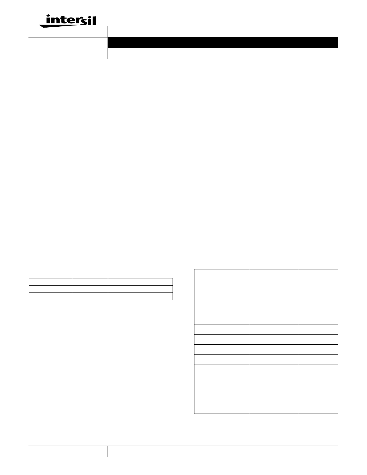
Pinouts
HS-245RH, HS-246RH, HS-248RH
HS9-245RH 14 PIN FLATPACK
HS1-245RH 14 CERAMIC DIP
MIL-STD-1835 CDIP2-T14
TOP VIEW
HS9-246RH/248RH 14 PIN FLATPACK
HS1-246RH/248RH 14 PIN CERAMIC DIP
MIL-STD-1835 CDFP3-F14
TOP VIEW
GND
1
2
T1
3
4
5
T2
6
7
T3
14
13
12
11
10
9
8
φ1 INPUT
φ1 OUTPUT
φ2 OUTPUT
φ2 INPUT
φ1 INPUT
φ1 OUTPUT
SUBSTRATE
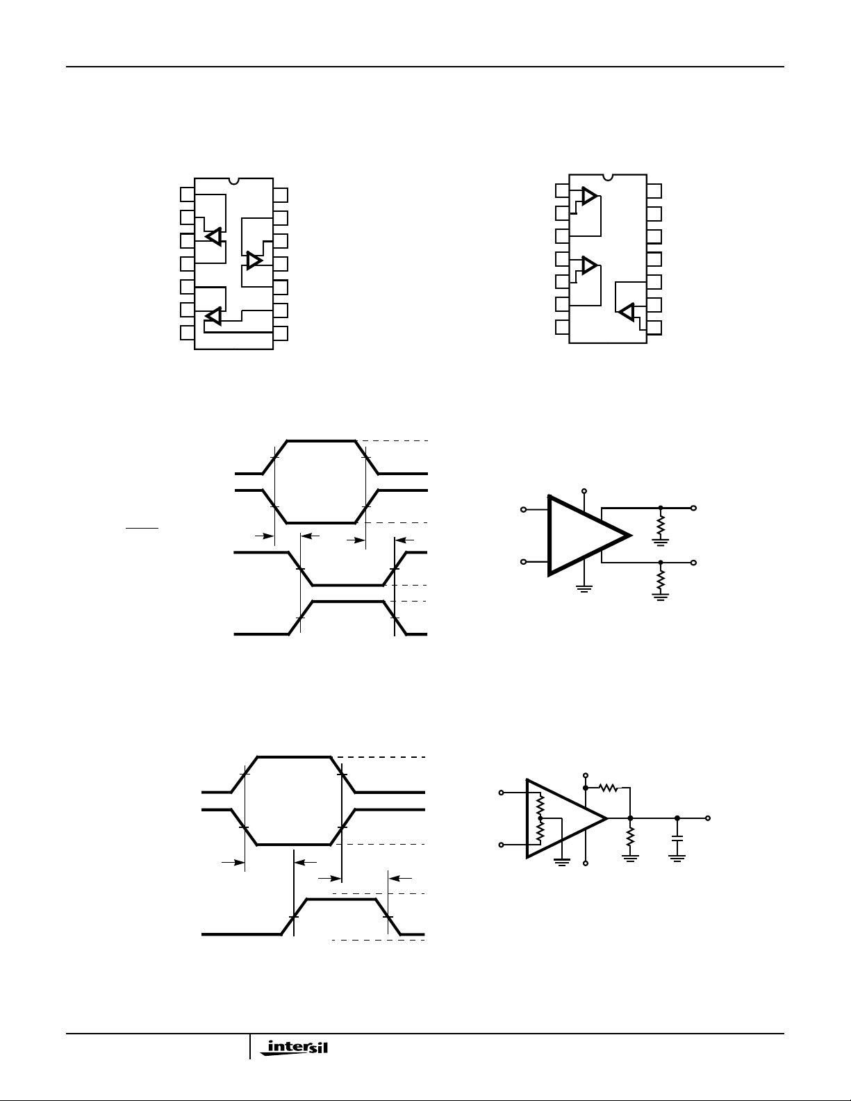
Test Circuits and Applications
NOTES:
Input: TTLH ≤ 10ns
TTHL ≤ 10ns
pw = 500ns
f = 1MHz
VOUT
IOUT =
50Ω
φ1 IN
φ2 IN
TPHL
φ1 OUT
φ2 OUT
VCC
INPUT
OUTPUT
OUTPUT
INPUT
INPUT
OUTPUT
φ2
φ1
φ2
φ2
φ1
φ2
TPLH
OPEN
(
≈3.2V)
0V
OPEN
(
≈3.2V)
0V
≈0.15V
≈3mA)
(
0V
≈0.15V
≈3mA)
(
0V
(-) INPUT
(+) INPUT
(R1) OUTPUT
(-) INPUT
(+) INPUT
(R2) OUTPUT
GND
φ1
φ2
1
2
3
4
5
6
7
D.U.T.
R1
R2
R3
VCC = +5V
VCC (R1 AND R2)
14
VCC (R3)
13
VEE (R1 AND R2)
12
VEE (R3)
11
OUTPUT (R3)
10
INPUT (+)
9
8
INPUT (-)
VOUT
50Ω
1%
TRANSMITTER
VOUT
50Ω
1%
φ1
OUT
φ2
NOTES:
Input: TTLH ≤ 10ns
TTHL ≤ 10ns
pw = 500ns
f = 1MHz
RECEIVER
All timing measurements referenced to 50% V points
(+)IN
(-) IN
OUT
All timing measurements referenced to 50% V points
FIGURE 1. CIRCUIT #1 TRANSMITTER PROPAGATION DELAY
150mV
0V
150mV
0V
TPLH
TPHL
5V
0V
(+)
(-)
FIGURE 2. CIRCUIT #2 RECEIVER PROPAGATION DELAY
2
50Ω
50
Ω
VCC = +5V
D.U.T.
VEE = - 5V
520Ω
800Ω
30pF
RECEIVER
OUTPUT
HS-245RH, HS-246RH, HS-248RH
Test Circuits and Applications (Continued)
+5V
IN
1/3
HS-245RH
ENABLE
NOTE: HS-245RH should be driven by open-collector
gates. (Totem-pole output may cause slight reduction in
“on” data current). For more detailed information, refer to
Design Information section of this data sheet.
(NOTE)
FIGURE 3. TYPICAL APPLICATION
Voltage Mode Transmission
Data rates of up to 10 million bits per second can be
obtained with standard TTL logic; however, the transmission
distance must be very short. For example, a typical 50 foot
low capacitance cable will have a capacitance of
approximately 750pF which requires a current of greater
than 50mA to drive 5V into this cable at 10MHz; therefore,
voltage mode transmitters are undesirable for long
transmission lines at high data rates due to the large current
required to charge the transmission line capacitance.
Current Mode Transmission
An alternate method of driving high data rates down long
transmission lines is to use a current mode transmitter.
Current mode logic changes the current in a low impedance
transmission line and requires very little change in voltage.
For example, a 2mA change in transmitter current will
produce a 100mV change in receiver voltage independent of
the series transmission line resistance. The rise time at the
receiver for a typical 50 foot cable (750pF) is approximately
30ns for a 2mA pulse.
+5V
1/3 HS-246RH
50Ω
50
Ω
-5V
“PARTY-LINE”
RECEIVER
-5V
RECEIVER
OUT
OUTPUT
(-)
(+)
(+)
(-)
+5V
1/3
HS-248RH
An emitter coupled logic gate is frequently used for a current
mode transmitter. However, ECL gates are not compatible
with TTL and DTL logic and they require considerable power.
The Intersil HS-245RH is a TTL/DTL compatible current
mode transmitter designed for high data rates on long
transmission lines. Data rates of 15 megabits per second
can be obtained with 50 feet of transmission line when using
the companion HS-246RH receiver. Data rates of 2 megabits
per second are easily obtained on transmission lines as long
as 1,000 feet. The Intersil transmitter and receivers feature
very low power, typically 25mW for the transmitter and
15mW for the receiver.
Intersil Transmitter/Receivers
The Intersil transmitter/receiver family consists of a triple line
transmitter,two triple line receivers with internal terminations
and a triple party-line receiver.The general characteristics of
the transmitter and receivers are outlined in Table A.
3

HS-245RH, HS-246RH, HS-248RH
TABLE A. GENERAL TRANSMITTER/RECEIVER CHARACTERISTICS
TRIPLE LINE TRANSMITTER
PARAMETER HS-245RH UNITS COMMENTS
Operating Temperature Range -55 to 125
“ON” Output Current 1.0 Min mA Over Full Temperature Range
Power Supply Current 7.0 Max mA Per Transmitter Section
Standby Current 33 Max µA Per Transmitter Section
Propagation Delay 14 Max ns Over Full Temperature Range
TRIPLE LINE RECEIVER
PARAMETER RECEIVER TYPE LIMITS UNITS COMMENTS
Operating Temperature Range HS-246RH/248RH -55 to 125
o
C
o
C
Power Supply
ICC (VCC = +5.0V)
Propagation Delay All Receivers 30 ns Over Full Temperature Range
Input Impedance and
Output Circuit
Transmitter
The HS-245RH transmitters have two inputs per transmitter,
HS-246RH/248RH 2.6 mA Per Receiver Section
INPUT
HS-246RH
HS-248RH Hi-Z 6K Pull-Up Resistor
100 Open Collector
IN
G1
Ω
G2
OUTPUT
either of which is low while the other is open during normal
operation and both inputs are open during standby. For
G3
optimum transmitter performance, the “off” input should be
open circuit rather than being pulled towards +5V, because
ENABLE
this will reduce the “on” output data current. On the other
hand, the “on” and “off” output data current will increase if
the “off” input is held below its open circuit voltage. Open
collector gates such as the 7401 and 7403 or 7405 HexInverter are suitable for driving the HS-245RH transmitter
inputs. By using 2-input gates as shown in Figure 6, an
1/3
HS-245RH
1/3
HS-246RH
enable line can be provided so that more than one
transmitter may be connected to a line for time sharing.
When the enable line is low the transmitter will be disabled
and will present a high impedance to the transmission line
as well as requiring very little power supply current.
Complementary input signals may be derived from high
speed inverter gates as shown, or by using the
+5 GND
2K-6K FOR TTL DRIVE
REQUIRED FOR HS-246RH
1/3
HS-248RH
-5V
+5VGND
complementary outputs of a flip-flop. When the transmitter is
connected near the midpoint of a long transmission line or to
a line with terminations at both ends, two transmitter
sections should be paralleled with respective inputs and
-5V+5VGND
outputs connected together in order to drive the reduced
impedance. This parallel transmitter technique can also be
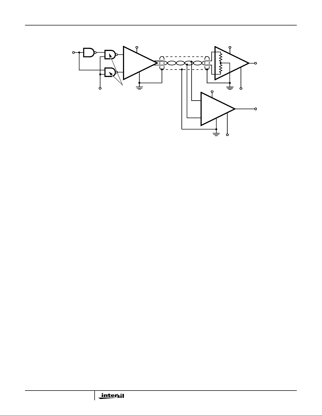
FIGURE 4. TYPICAL DATA TRANSMISSION SYSTEM
used to increase the data rate on long transmission lines.
OUT
OUT
4

HS-245RH, HS-246RH, HS-248RH
Transmitter Operation
The transmitter alternately applies the current to each of the
two conductors in the twisted pair line such that the total
current in the twisted pair is constant and alwaysin the same
direction. This current flows through either of the two 50V
terminating resistors at the receiver and returns to the
transmitter as a steady DC current on the transmission line
shield. The DC power supply return for the transmitter is
through the receiver terminating resistors (the transmitter
ground pin is only a substrate ground). Therefore, it is
essential that the shield be connected to the power supply
common at both the transmitter and receiver, preferably at
the integrated circuit “ground” pin. More than fifteen twisted
pair lines can share the same shield without crosstalk.
Receivers
The HS-248RH “party-line” receiver presents a high
impedance load to the transmission line allowing as many as
ten HS-248RH receivers to be distributed along a line without
excessive loading. Figure 6 shows a typical system of a
transmitter, a terminating receiver and a party-line receiver.
The transmission line is terminated in its characteristics
impedance by an HS-246RH or by a pair of 50Ω resistors
connecting each line to the ground return shield.
Transmission Lines
The maximum frequency (or minimum pulse width) which
can be carried by a certain length of a given transmission
line is dependent on the loss characteristics of the particular
line. At low frequencies, there will be virtually no loss in
pulse amplitude, but there will be a degradation of rise and
fall-time which is roughly proportional to the square of the
line length. This is shown in Figure 7. If the pulse width is
less than the rise-time at the receiver end, the pulse
amplitude will be diminished, approaching the point where it
cannot be detected by the receiver.
150mV
LINE
VOLTAGE
AT TRANS-
MITTER
TTLH1 TTHL1
150mV
LINE
VOLTAGE
AT
RECEIVER
TTLH2
WIDE PULSE
TRLH2 = TTLH1 KL
TTHL2 = TTHL1 KL
FIGURE 5. TRANSMISSION LINE WAVE-SHAPING
TTHL2
2
2
0V
TTLH2 TTHL1
0V
TTLH2 TTHL2
MINIMUM PULSE WIDTH
Where: L is Line Length K is
determined by line loss
characteristics
The transmission line used with the Intersil HS-245RH
series transmitter and receivers can be any ordinary
shielded, twisted pair line with a characteristic impedance of
100Ω. Twisted pair lines consisting of number 20 or 22
gauge wire will generally havethis characteristic impedance.
Special high quality transmission lines are not necessary
and standard audio, shielded-twisted pair, cable is generally
suitable.
Since the necessary characteristics for various twisted pair
lines are not readily available, it may be necessary to take
some measurements on a length of the proposed line. Todo
this, connect an HS-245RH transmitter to one end of the line
(100 feet or more) and an HS-246RH to the other end. The
rise and fall-times can be measured on the line at both ends
and the constant ‘‘K’’, for that line can be computed as
shown in Figure 7 so that the minimum pulse width can be
determined for any length of line.
Data rates of 2MHz have been obtained using 1,000 feet of
standard shielded, twisted pair, audio cable. Data rates of
15MHz are possible on shorter lengths of transmission line
(50 feet).
Electromagnetic Interference
Very little electromagnetic interference is generated by the
Intersil current mode system because the total current
through the twisted pair is constant, while the current
through the shield is also constant and in the opposite
direction. This can be verified by observing, with a current
probe, the total current through the twisted pair, through the
shield and through the complete shielded, twisted pair cable.
In each case a constant current will be observed with only
small variations. Small pulses may be observed if the
complementary inputs to the transmitter do not switch at the
same time. The current will decrease during the time both
inputs are high, and will increase during the time both inputs
are low. These switching pulses may be observed when
using the circuit shown in Figure 6. The amplitude and shape
of these pulses will depend of the propagation delay of G1,
and transition times G2 and G3. These pulses are generally
of no concern because of their small amplitude and width,
but they may be reduced by increasing the similarity of the
waveforms and timing synchronization of the complementary
signals applied to the transmitter.
In addition to generating very little noise, the system is also
highly immune to outside noise since it is difficult to
capacitively couple a differential signal into the low
impedance twisted pair cable and it is even more difficult in
induce a differential current into the line due to the very high
impedance of the constant current transmitter. Therefore,
differential mode interference is generally not a problem with
the Intersil current mode system. Large common mode
voltages can also be tolerated because the output current of
the transmitter is constant as long as the receiver
termination ground is less than 2V positive with respect to
5

HS-245RH, HS-246RH, HS-248RH
the grounded input of the transmitter, and is less than 25V
negative with respect to the transmitter VCC. The current
mode system is totally unaffected by ground differential
noise of +2V at frequencies as high as 1MHz.
Propagation Delay
The worst case propagation delay of a transmitter and
receiver, connected as shown in Figure 6, can be
determined by adding the maximum delay shown on the
data sheet for the transmitter and receiver. These overall
switching characteristics are shown in TableB. For the entire
system, however, the propagation delay of the transmission
line must also be considered. This delay, of course, depends
on the length of the line and the characteristics of the line,
Schematics
2.7K 2.7K
380Ω
but in general, delays of between 1.5ns and 3.0ns per foot
can be expected.
TABLE B. OVERALL TRANSMITTER/RECEIVER SWITCHING
CHARACTERISTICS
-55oC TO 125oC
HS-245RH, HS-246RH
HS-248RH
CHARACTERISTICS
Propagation Delay
TPLH
Propagation Delay
TPHL
Duty Cycle Distortion
TPLH - TPHL
NOTE: VCC = +5V, VEE = -5V.
14VCC
-1840ns
-1840ns
- 2 15 ns
UNITSMIN TYP MAX
(R1) +INPUT
GND
300Ω
2.0K 2.0K
12 34
φ1
φ1
IN
OUTφ2INφ2OUT
T1
56 89
φ1INφ1
OUTφ2INφ2OUT
T2
10 11 12 13
φ1INφ1
OUTφ2INφ2OUT
T3
FIGURE 6. HS-245RH
14VCC
(R1) OUTPUT
1
(R1)
50Ω
3
+INPUT
-INPUT
5
(R2)
12VEE 11VEE
6K
4.1K
-INPUT
2
50Ω
7
2.7K
6
+INPUT
4
(R2)
13VCC
10
(R3) OUTPUT(R2) OUTPUT
-INPUT
9
(R3)
8
(R3)
R1
FIGURE 7. HS-246RH, HS-248RH
NOTES:
1. HS-246RH does not have 6K output pull-up resistors.
2. HS-248RH does not have 50Ω input termination resistors.
6
R2 R3

Die Characteristics
HS-245RH
DIE DIMENSIONS:
45 mils x 45 mils x 11 mils
1140µm x 1140µm x 280µm
INTERFACE MATERIALS:
Glassivation:
Type: Silox
Thickness: 8k
Å ±1kÅ
Top Metallization:
Type: Aluminum
Thickness: 12.5k
Å ±2kÅ
Substrate:
HFSB Bipolar/Dielectric Isolation
Backside Finish:
Silicon
Metallization Mask Layout
HS-245RH
OUTPUT f1
INPUT f1
ASSEMBLY RELATED INFORMATION:
Substrate Potential:
Unbiased
ADDITIONAL INFORMATION:
Worst Case Current Density:
4
2
7.8 x 10
A/cm
Transistor Count:
6
VCC
INPUT f2
OUTPUT f2
INPUT f2
INPUT f1
OUTPUT f1
SUBSTRATE
GND
INPUT f2
OUTPUT f2
OUTPUT f2
OUTPUT f1
INPUT f1
7

Die Characteristics
HS-246RH, HS-248RH
DIE DIMENSIONS:
45 mils x 47 mils x 11 mils
1140µm x 1190µm x 280µm
INTERFACE MATERIALS:
Glassivation:
Type: Silox
Thickness: 8k
Å ±1kÅ
Top Metallization:
Type: T.W.
Thickness: 2.5k
Å ±0.5kÅ
Type: Al
Thickness: 14k
Å ±2kÅ
Substrate:
ALPS Bipolar/Dielectric Isolation
Backside Finish:
Silicon
Metallization Mask Layout
HS-246RH HS-248RH
ASSEMBLY RELATED INFORMATION:
Substrate Potential:
Unbiased
ADDITIONAL INFORMATION:
Worst Case Current Density:
5
2
1.4 x 10
A/cm
Transistor Count:
9
(+) INPUT
(-) INPUT
VCC R1 AND R2
OUTPUT R1
(-) INPUT
(+) INPUT
3
GND
OUTPUT R2
(-) INPUT
VCC R3
VEE R1 AND R2
VEE R3
OUTPUT R3
(+) INPUT
OUTPUT R1
(-) INPUT
(+) INPUT
(+) INPUT
(-) INPUT
GND
OUTPUT R2
VCC R1 AND R2
VCC R3
(-) INPUT
(+) INPUT
VEE R1 AND R2
VEE R3
OUTPUT R3
All Intersil semiconductor products are manufactured, assembled and tested under ISO9000 quality systems certification.
Intersil semiconductor products are sold by description only. Intersil Corporation reserves the right to make changes in circuit design and/or specifications at any time without notice. Accordingly, the reader is cautioned to verify that data sheets are current before placing orders. Information furnished by Intersil is believed to be accurate and
reliable. However ,no responsibility is assumed by Intersil or its subsidiaries for its use; nor for any infringements of patents or other rights of third parties which may result
from its use. No license is granted by implication or otherwise under any patent or patent rights of Intersil or its subsidiaries.
For information regarding Intersil Corporation and its products, see web site http://www.intersil.com
8
 Loading...