

Datasheet HS-307RH-883S, HS-384RH-883S, HS-390RH-883S, HS-302RH-883S, HS-303RH-883S Datasheet (Intersil Corporation)
...Page 1
September 1995
HS-302RH/883S, HS-303RH/883S,
HS-306RH/883S, HS-307RH/883S,
HS-384RH/883S, HS-390RH/883S
Radiation Hardened
CMOS Analog Switches
Features
• This Circuit is Processed in Accordance to Mil-Std883 and is Fully Conformant Under the Provisions of
Paragraph 1.2.1.
• Radiation Hardened
- Functional Total Dose Exceeds 1 x 10
• Pin for Pin Compatible with Intersil HI-3XX Series
Analog Switches
• Analog Signal Range 15V
• Low Leakage
•Low R
• No Latch Up
• Versions for 5V and 15V Digital Systems
• Low Operating Power
• Military Temperature Range -55
ON
o
C to +125oC
5
RAD Si
Applications
• Sample and Hold i.e. Low Leakage Switching
• Op Amp Gain Switching i.e. Low ON Resistance
• Switched Capacitor Filters
• Low Level Switching Circuits
• Satellites
• Nuclear Reactor Controls
• Military Environments
Description
The HS-3XXRH/883S family of analog switches are
monolithic devices fabricated using Radiation Hardened
CMOS technology and the Intersil dielectric isolation process for latch-up free operation. Improved total dose hardness is obtained by layout (thin oxide tabs extending to a
channel stop) and processing (hardened gate oxide). These
switches offer low-resistance switching performance for analog voltages up to the supply rails. “ON” resistance is low
and stays reasonably constant over the full range of operating voltage and current. “ON” resistance also stays reasonably constant when exposed to radiation, being typically 30Ω
pre-rad and 35Ω post 100K RAD-Si. All devices provide
break-before-make switching.
The 6 devices in this switch series are differentiated by type
of switch action, pinout and digital logic levels. The HS-302/
303/384/390RH/883S switches have 5V digital inputs while
the HS-306/307RH/883S switches have 15V digital inputs.
All devices are available in Ceramic Flatpack and SBDIP
packages. The HS-3XXRH/883S switches can directly
replace the HI-3XX series devices.
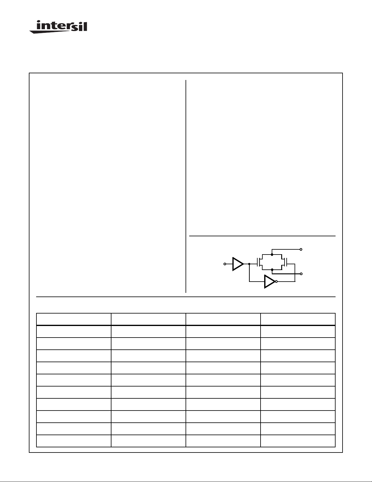
Functional Diagram
IN
N P
D
Ordering Information
PART NUMBER TEMPERATURE RANGE SCREENING LEVEL PACKAGE
HS1-302RH/883S -55oC to +125oC Intersil /883 Class S Equivalent 14 Lead SBDIP
HS9-302RH/883S -55oC to +125oC Intersil /883 Class S Equivalent 14 Lead Ceramic Flatpack
HS1-302RH/Sample +25oC Sample 14 Lead SBDIP
HS9-302RH/Sample +25oC Sample 14 Lead Ceramic Flatpack
HS1-303RH/883S -55oC to +125oC Intersil /883 Class S Equivalent 14 Lead SBDIP
HS9-303RH/883S -55oC to +125oC Intersil /883 Class S Equivalent 14 Lead Ceramic Flatpack
HS1-303RH/Sample +25oC Sample 14 Lead SBDIP
HS9-303RH/Sample +25oC Sample 14 Lead Ceramic Flatpack
HS1-306RH/883S ( Note 1) -55oC to +125oC Intersil /883 Class S Equivalent 14 Lead SBDIP
HS9-306RH/883S ( Note 1) -55oC to +125oC Intersil /883 Class S Equivalent 14 Lead Ceramic Flatpack
CAUTION: These devices are sensitive to electrostatic discharge; follow proper IC Handling Procedures.
http://www.intersil.com or 407-727-9207 | Copyright © Intersil Corporation 1999
1
Spec Number 518526
File Number 3067.1
Page 2
HS-3XXRH/883S
Ordering Information
(Continued)
PART NUMBER TEMPERATURE RANGE SCREENING LEVEL PACKAGE
HS1-306RH/Sample (Note 1) +25oC Sample 14 Lead SBDIP
HS9-306RH/Sample (Note 1) +25oC Sample 14 Lead Ceramic Flatpack
HS1-307RH/883S -55oC to +125oC Intersil /883 Class S Equivalent 14 Lead SBDIP
HS9-307RH/883S -55oC to +125oC Intersil /883 Class S Equivalent 14 Lead Ceramic Flatpack
HS1-307RH/Sample +25oC Sample 14 Lead SBDIP
HS9-307RH/Sample +25oC Sample 14 Lead Ceramic Flatpack
HS1-384RH/883S (Note 1) -55oC to +125oC Intersil /883 Class S Equivalent 16 Lead SBDIP
HS9-384RH/883S (Note 1) -55oC to +125oC Intersil /883 Class S Equivalent 16 Lead Ceramic Flatpack
HS1-384RH/Sample (Note 1) +25oC Sample 16 Lead SBDIP
HS9-384RH/Sample (Note 1) +25oC Sample 16 Lead Ceramic Flatpack
HS1-390RH/883S -55oC to +125oC Intersil /883 Class S Equivalent 16 Lead SBDIP
HS9-390RH/883S -55oC to +125oC Intersil /883 Class S Equivalent 16 Lead Ceramic Flatpack
HS1-390RH/Sample +25oC Sample 16 Lead SBDIP
HS9-390RH/Sample +25oC Sample 16 Lead Ceramic Flatpack
NOTE:
1. Not recommended for new design.
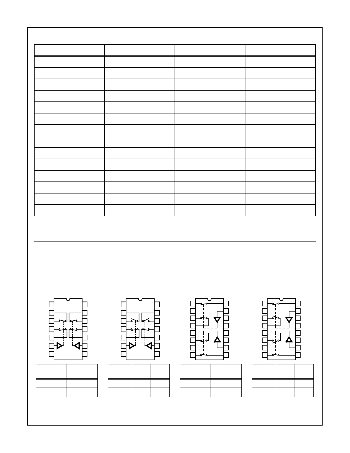
Pinouts
NC
S3
D3
D1
S1
IN1
GND
LOGIC
(Switch States are for Logic “1” Inputs)
14 LEAD CERAMIC DUAL-IN-LINE
METAL SEAL PACKAGE (SBDIP)
MIL-STD-1835 CDIP2-T14
TOP VIEW
DUAL DPST
HS-302RH/883S
HS-306RH/883S
1
2
3
4
5
6
7
14
V+
13
S4
12
D4
11
D2
10
S2
9
IN2
8
V-
GND
SWITCH
1 - 4
0 OFF
1ON
DUAL SPDT
HS-303RH/883S
HS-307RH/883S
1
NC
2
S3
3
D3
4
D1
5
S1
6
IN1
7
SW1
LOGIC
SW2
0 OFF ON
1 ON OFF
14
13
12
11
10
9
8
SW3
SW4
V+
S4
D4
D2
S2
IN2
V-
16 LEAD CERAMIC DUAL-IN-LINE
METAL SEAL PACKAGE (SBDIP)
MIL-STD-1835 CDIP2-T16
DUAL DPST
HS-384RH/883S
D1
NC
D3
S3
S4
D4
NC
D2
1
2
3
4
5
6
7
8
16
15
14
13
12
11
10
9
SWITCH
LOGIC
1 - 4
0 OFF
1ON
TOP VIEW
S1
IN1
VGND
NC
V+
IN2
S2
DUAL SPDT
HS-390RH/883S
1
D1
2
NC
3
D3
4
S3
5
S4
6
D4
7
NC
8
D2
SW1
LOGIC
SW2
0 OFF ON
1 ON OFF
16
15
14
13
12
11
10
9
S1
IN1
VGND
NC
V+
IN2
S2
SW3
SW4
Spec Number 518526
2
Page 3
HS-3XXRH/883S
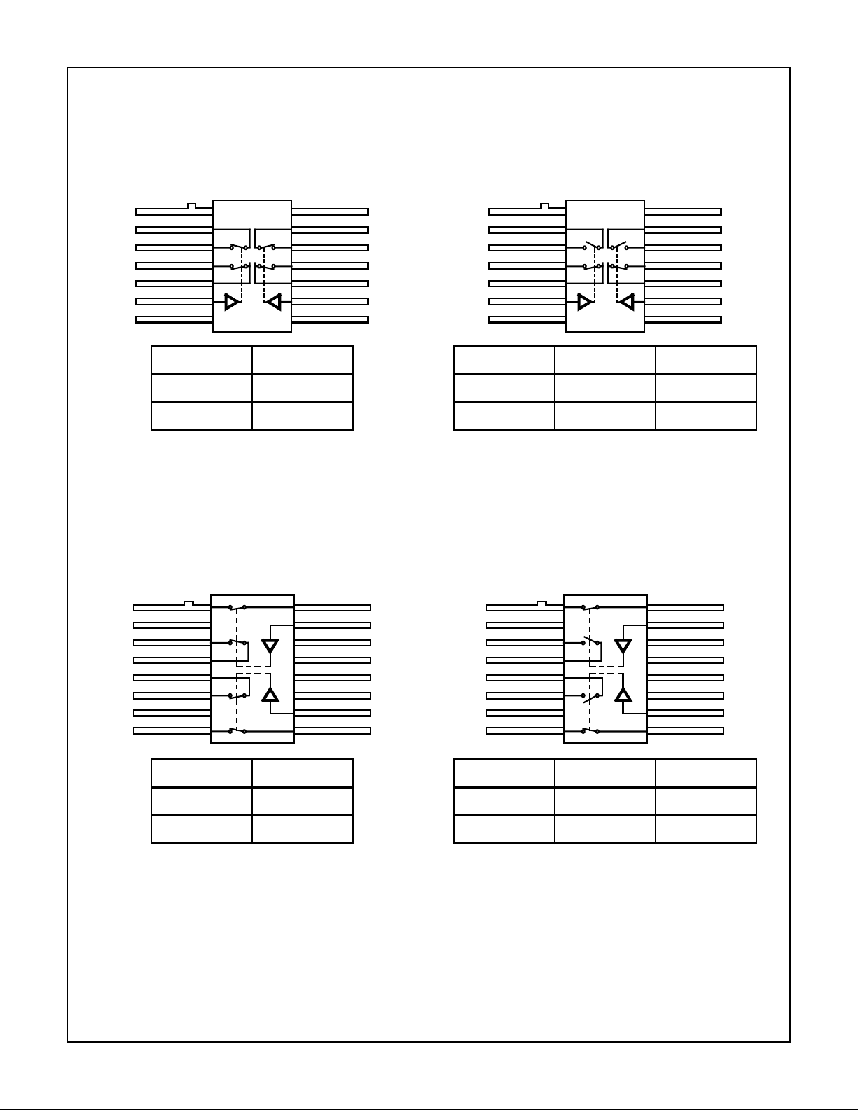
Pinouts
NC
S3
D3
D1
S1
IN1
GND
(Switch States are for Logic “1” Inputs) (Continued)
14 LEAD CERAMIC METAL SEAL FLATPACK PACKAGE (FLATPACK)
MIL-STD-1835 CDIP3-F14
DUAL DPST
HS-302RH/883S
HS-306RH/883S
1
2
3
4
5
6
7
14
13
12
11
10
9
8
V+
S4
D4
D2
S2
IN2
V-
LOGIC SWITCH 1 - 4
0 OFF
1ON
TOP VIEW
DUAL SPDT
HS-303RH/883S
HS-307RH/883S
NC
S3
D3
D1
S1
IN1
GND
1
2
3
4
5
6
7
14
13
12
11
10
9
8
LOGIC SW1 AND SW2 SW3 AND SW4
0 OFF ON
1 ON OFF
V+
S4
D4
D2
S2
IN2
V-
D1
NC
D3
S3
S4
D4
NC
D2
16 LEAD CERAMIC METAL SEAL FLATPACK PACKAGE (FLATPACK)
DUAL DPST
HS-384RH/883S
116
2
3
4
5
6
7
8
15
14
13
12
11
10
9
LOGIC SWITCH 1 - 4
0 OFF
1ON
MIL-STD-1835 CDIP4-F16
TOP VIEW
S1
IN1
VGND
NC
V+
IN2
S2
D1
NC
D3
S3
S4
D4
NC
D2
DUAL SPDT
HS-390RH/883S
116
2
3
4
5
6
7
8
15
14
13
12
11
10
9
S1
IN1
VGND
NC
V+
IN2
S2
LOGIC SW1 AND SW2 SW3 AND SW4
0 OFF ON
1 ON OFF
Spec Number 518526
3
Page 4
Specifications HS-3XXRH/883S
Absolute Maximum Ratings Reliability Information
Supply Voltage Between V+ and V- . . . . . . . . . . . . . . . . . . . . . +44V
+VSUPPLY to Ground . . . . . . . . . . . . . . . . . . . . . . . . . . . . . . . +22V
-VSUPPLY to Ground. . . . . . . . . . . . . . . . . . . . . . . . . . . . . . . . .-22V
Analog Input Overvoltages:
+VS. . . . . . . . . . . . . . . . . . . . . . . . . . . . . . . . . . +VSUPPLY +1.5V
-VS . . . . . . . . . . . . . . . . . . . . . . . . . . . . . . . . . . .-VSUPPLY - 1.5V
Digital Input Overvoltage:
+VA. . . . . . . . . . . . . . . . . . . . . . . . . . . . . . . . . . . .+VSUPPLY +4V
-VA . . . . . . . . . . . . . . . . . . . . . . . . . . . . . . . . . . . . .-VSUPPLY -4V
Peak Current, S or D Pulsed at 1ms, 10% Duty Cycle Max. . .40mA
Continuous Current . . . . . . . . . . . . . . . . . . . . . . . . . . . . . . . . .10mA
Storage Temperature Range . . . . . . . . . . . . . . . . . -65oC to +150oC
Junction Temperature. . . . . . . . . . . . . . . . . . . . . . . . . . . . . . +175oC
Lead Temperature (soldering 10s) . . . . . . . . . . . . . . . . . . . . .≤ +300oC
CAUTION: Stresses above those listed in “Absolute Maximum Ratings” may cause permanent damage to the device. This is a stress only rating and operation
of the device at these or any other conditions above those indicated in the operational sections of this specification is not implied.
Operating Conditions
Operating Supply Voltage (± VSupply) . . . . . . . . . . . . . . . . . . . . . ±15V Operating Temperature Range . . . . . . . . . . . . . . . .-55oC to +125oC
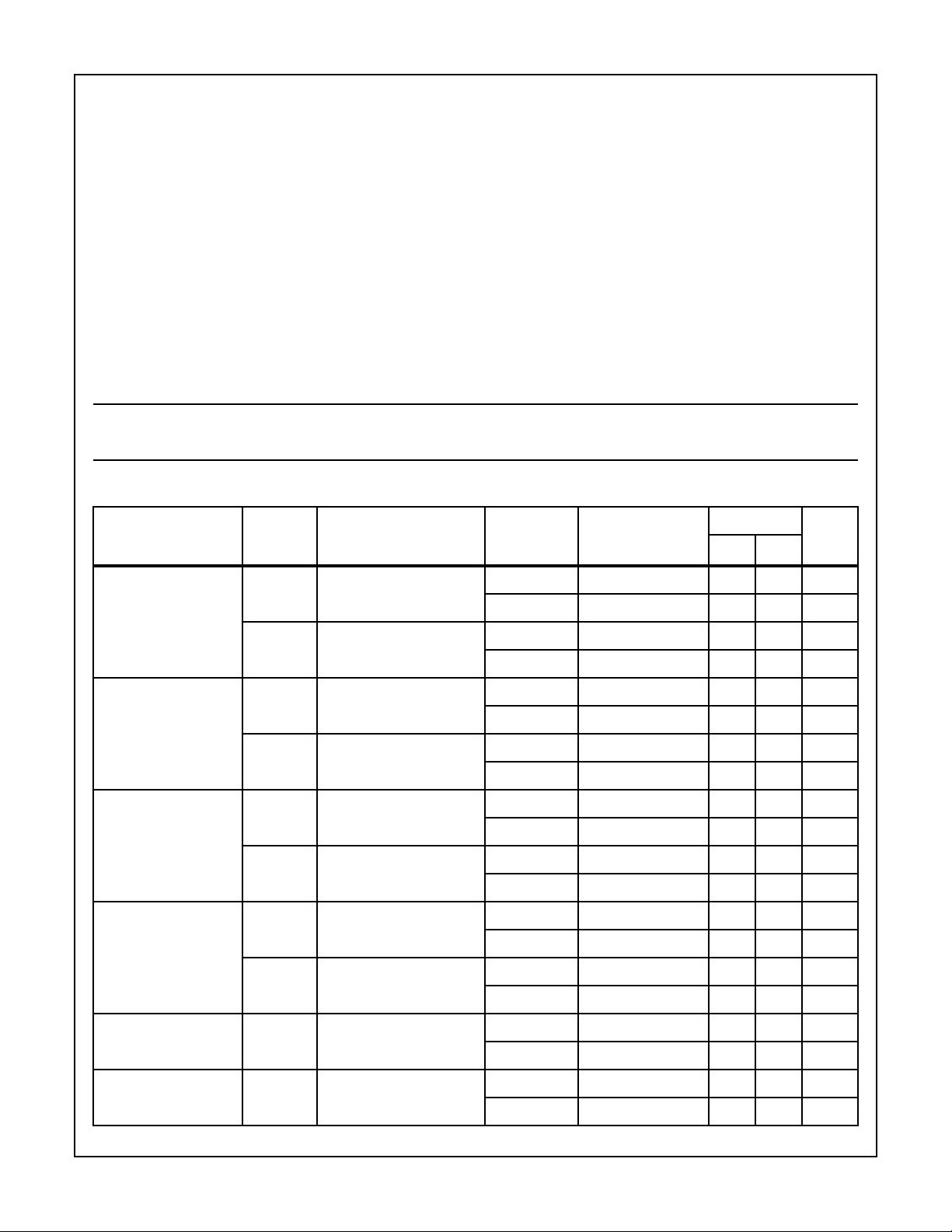
TABLE 1. HS-302RH/303RH/384RH/390RH/883S DC ELECTRICAL PERFORMANCE CHARACTERISTICS
Device Guaranteed and 100% Tested. Unless Otherwise Specified: V- = -15V, V+ = +15V, VAH = +4.0V, VAL = 0.8V
PARAMETER SYMBOL CONDITIONS
Thermal Resistance θ
14 Lead SBDIP Package. . . . . . . . . . . . . 70oC/W 19oC/W
14 Lead Ceramic Flatpack Package . . . . 105oC/W 17oC/W
16 Lead SBDIP Package. . . . . . . . . . . . . 70oC/W 19oC/W
16 Lead Ceramic Flatpack Package . . . . 105oC/W 17oC/W
Maximum Package Power Dissipation at +125oC Ambient
14 Lead SBDIP Package. . . . . . . . . . . . . . . . . . . . . . . . . . . 0.71W
14 Lead Ceramic Flatpack Package . . . . . . . . . . . . . . . . . . 0.48W
16 Lead SBDIP Package. . . . . . . . . . . . . . . . . . . . . . . . . . . 0.71W
16 Lead Ceramic Flatpack Package . . . . . . . . . . . . . . . . . . . .0.48
If device power exceeds package dissipation capability, provide heat
sinking or derate linearly at the following rate:
14 Lead SBDIP Package. . . . . . . . . . . . . . . . . . . . . . .14.3mW/oC
14 Lead Ceramic Flatpack Package . . . . . . . . . . . . . . . 9.5mW/oC
16 Lead SBDIP Package. . . . . . . . . . . . . . . . . . . . . . .14.3mW/oC
16 Lead Ceramic Flatpack Package . . . . . . . . . . . . . . . 9.5mW/oC
GROUP A
SUB-
GROUPS TEMPERATURE
JA
LIMITS
θ
JC
UNITSMIN MAX
“Switch On” Resistance +RDS VD = 10V, IS = -10mA,
S1/S2/S3/S4
-RDS VD = -10V, IS = 10mA,
S1/S2/S3/S4
Leakage Current Into
the Source Terminal of
an “Off” Switch
Leakage Current into
theDrainTerminalofan
“Off” Switch
Leakage Current from
an “On” Driver Into the
Switch (Drain&Source)
Low Level Input
Address Current
+IS(OFF) VS = +14V, VD = -14V,
S1/S2/S3/S4
-IS(OFF) VS = -14V, VD = +14V,
S1/S2/S3/S4
+ID(OFF) VS = -14V, VD = +14V,
S1/S2/S3/S4
-ID(OFF) VS = +14V, VD = -14V,
S1/S2/S3/S4
+ID(ON) VS = VD = +14V,
S1/S2/S3/S4
-ID(ON) VS = VD = -14V,
S1/S2/S3/S4
IAL All Channels VA = 0.8V 1 +25oC-11µA
1 +25oC-50Ω
2, 3 -55oC to +125oC-75Ω
1 +25oC-50Ω
2, 3 -55oC to +125oC-75Ω
1 +25oC-22nA
2, 3 -55oC to +125oC -100 100 nA
1 +25oC-22nA
2, 3 -55oC to +125oC -100 100 nA
1 +25oC-22nA
2, 3 -55oC to +125oC -100 100 nA
1 +25oC-22nA
2, 3 -55oC to +125oC -100 100 nA
1 +25oC-22nA
2, 3 -55oC to +125oC -100 100 nA
1 +25oC-22nA
2, 3 -55oC to +125oC -100 100 nA
2, 3 -55oC to +125oC-11 µA
High Level Input
Address Current
IAH All Channels VA = 4.0V 1 +25oC-11µA
2, 3 -55oC to +125oC-11 µA
Spec Number 518526
4
Page 5
Specifications HS-3XXRH/883S
TABLE 1. HS-302RH/303RH/384RH/390RH/883S DC ELECTRICAL PERFORMANCE CHARACTERISTICS
Device Guaranteed and 100% Tested. Unless Otherwise Specified: V- = -15V, V+ = +15V, VAH = +4.0V, VAL = 0.8V (Continued)
GROUP A
SUB-
PARAMETER SYMBOL CONDITIONS
Positive Supply Current I(+) All Channels VA = 0.8V 1 +25oC-10µA
GROUPS TEMPERATURE
2, 3 -55oC to +125oC - 100 µA
LIMITS
UNITSMIN MAX
VA1 = 0V, VA2 = 4.0V and
VA1 = 4.0V, VA2 = 0V
Negative Supply
Current
TABLE 1. HS-306RH/307RH/883S DC ELECTRICAL PERFORMANCE CHARACTERISTICS
Device Guaranteed and 100% Tested. Unless Otherwise Specified: V- = -15V, V+ = +15V, VAH = +11.0V, VAL = 3.5V
PARAMETER SYMBOL CONDITIONS
“Switch On” Resistance +RDS VD = 10V, IS = -10mA,
Leakage Current Into
the Source Terminal of
an “Off” Switch
I(-) All Channels VA = 0.8V 1 +25oC -10 - µA
VA1 = 0V, VA2 = 4.0V and
VA1 = 4.0V, VA2 = 0V
S1/S2/S3/S4
+RDS VD = -10V, IS = 10mA,
S1/S2/S3/S4
+IS(OFF) VS = +14V, VD = -14V,
S1/S2/S3/S4
1 +25oC - 0.5 mA
2, 3 -55oC to +125oC-1mA
2, 3 -55oC to +125oC -100 - µA
1 +25oC -10 - µA
2, 3 -55oC to +125oC -100 - µA
GROUP A
SUB-
GROUPS TEMPERATURE
1 +25oC-50Ω
2, 3 -55oC to +125oC-75Ω
1 +25oC-50Ω
2, 3 -55oC to +125oC-75Ω
1 +25oC-22nA
2, 3 -55oC to +125oC -100 100 nA
LIMITS
UNITSMIN MAX
Leakage Current into
theDrainTerminalofan
“Off” Switch
Leakage Current from
an “On” Driver Into the
Switch (Drain and
Source)
Low Level Input
Address Current
High Level Input
Address Current
-IS(OFF) VS = -14V, VD = +14V,
S1/S2/S3/S4
+ID(OFF) VS = -14V, VD = +14V,
S1/S2/S3/S4
-ID(OFF) VS = +14V, VD = -14V,
S1/S2/S3/S4
+ID(ON) VS = VD = +14V,
S1/S2/S3/S4
-ID(ON) VS = VD = -14V,
S1/S2/S3/S4
IAL All Channels VA = 3.5V 1 +25oC-11µA
IAH All Channels VA = 11V 1 +25oC-11µA
1 +25oC-22nA
2, 3 -55oC to +125oC -100 100 nA
1 +25oC-22nA
2, 3 -55oC to +125oC -100 100 nA
1 +25oC-22nA
2, 3 -55oC to +125oC -100 100 nA
1 +25oC-22nA
2, 3 -55oC to +125oC -100 100 nA
1 +25oC-22nA
2, 3 -55oC to +125oC -100 100 nA
1, 2 -55oC to +125oC-11 µA
1, 2 -55oC to +125oC-11 µA
Spec Number 518526
5
Page 6
Specifications HS-3XXRH/883S
TABLE 1. HS-306RH/307RH/883S DC ELECTRICAL PERFORMANCE CHARACTERISTICS
Device Guaranteed and 100% Tested. Unless Otherwise Specified: V- = -15V, V+ = +15V, VAH = +11.0V, VAL = 3.5V (Continued)
GROUP A
SUB-
PARAMETER SYMBOL CONDITIONS
Positive Supply Current I(+) All Channels VA = 0V 1 +25oC-10µA
All Channels VA = 15V 1 +25oC-10µA
Negative Supply
Current
TABLE 2. HS-302RH/303RH/384RH/390RH/883S AC ELECTRICAL PERFORMANCE CHARACTERISTICS
Device Guaranteed and 100% Tested. Unless Otherwise Specified: V- = -15V, V+ = +15V, VAH = +4.0V, VAL = 0V
PARAMETER SYMBOL CONDITIONS
Break-Before-Make
TimeDelay(HS-303RH
& 390RH Only)
I(-) All Channels VA = 0V 1 +25oC -10 - µA
All Channels VA = 15V 1 +25oC -10 - µA
TOPEN RL = 300Ω, VS = +3V,
VAH = 5V
GROUPS TEMPERATURE
2, 3 -55oC to +125oC - 100 µA
2, 3 -55oC to +125oC - 100 µA
2, 3 -55oC to +125oC -100 - µA
2, 3 -55oC to +125oC -100 - µA
GROUP A
SUB-
GROUPS TEMPERATURE
9 +25oC 30 150 ns
10, 11 -55oC to +125oC - 300 ns
LIMITS
LIMITS
UNITSMIN MAX
UNITSMIN MAX
Switch Turn “On” Time TON RL = 300Ω, VS = +3V 9 +25oC - 300 ns
10, 11 -55oC to +125oC - 500 ns
Switch Turn “Off” Time TOFF RL = 300Ω, VS = +3V 9 +25oC - 250 ns
10, 11 -55oC to +125oC - 450 ns
TABLE 2. HS-306RH/307RH/883S AC ELECTRICAL PERFORMANCE CHARACTERISTICS
Device Guaranteed and 100% Tested. Unless Otherwise Specified: V- = -15V, V+ = +15V, VAH = +15.0V, VAL = 0V
GROUP A
SUB-
PARAMETER SYMBOL CONDITIONS
Break-Before-Make
TimeDelay(HS-307RH
Only)
Switch Turn “On” Time TON RL = 300Ω, VS = +3V 9 +25oC - 300 ns
Switch Turn “Off” Time TOFF RL = 300Ω, VS = +3V 9 +25oC - 250 ns
TOPEN RL = 300Ω, VS = +3V 9 +25oC 30 150 ns
GROUPS TEMPERATURE
10, 11 -55oC to +125oC - 300 ns
10, 11 -55oC to +125oC - 500 ns
10, 11 -55oC to +125oC - 450 ns
LIMITS
UNITSMIN MAX
Spec Number 518526
6
Page 7
Specifications HS-3XXRH/883S
TABLE 3. HS-302RH/303RH/306RH/307RH/384RH/390RH/883S
ELECTRICAL PERFORMANCE CHARACTERISTICS (NOTE 1)
Unless Otherwise Specified: HS-302RH/303RH/384RH/390RH/883S V- = -15V, V+ = +15V, VAH = +4.0V, VAL = 0V
HS-306RH/307RH/883S V- = -15V, V+ = +15V, VAH = +15.0V, VAL = 0V
(NOTE 1)
PARAMETER SYMBOL
Switch Input Capacitance CIS(OFF) Measured Source to GND +25oC - 28 pF
Driver Input Capacitance CC1 VA = 0V +25oC - 10 pF
CC2 VA = 15V +25oC - 10 pF
Switch Output COS Measured Drain to GND +25oC - 28 pF
Off Isolation VISO VGEN = 1Vp-p, f = 1MHz +25oC40-dB
Crosstalk VCR VGEN = 1Vp-p, f = 1MHz +25oC40-dB
Charge Transfer VCTE VS = GND, CL = 0.01µF +25oC - 15 mV
NOTE:1. Parameterslisted in Table 3are controlled viadesignor processparametersand arenotdirectly tested atfinalproduction. These
parameters are lab characterized upon initial design release, or upon design changes. These parameters are guaranteed by
characterization based upon data from multiple production runs which reflect lot to lot and within lot variation.
TABLE 4. HS-302RH/303RH/384RH/390RH/883S DC POST 100K RAD (Si) ELECTRICAL CHARACTERISTICS
Tested Per Mil-Std-883. Unless Otherwise Specified: HS-302RH/303RH/384RH/390RH/883S V- = -15V, V+ = +15V, VAH = +4.0V, VAL = 0.8V
CONDITIONS TEMPERATURE
LIMITS
UNITSMIN MAX
LIMITS
PARAMETER SYMBOL CONDITIONS TEMPERATURE
“Switch On” Resistance +RDS VD = 10V, IS = -10mA, S1/S2/S3/S4 +25oC-60Ω
-RDS VD = -10V, IS = 10mA, S1/S2/S3/S4 +25oC-60Ω
Leakage Current Into the
Source Terminal of an “Off”
Switch
LeakageCurrentinto theDrain
Terminal of an “Off” Switch
Leakage Current from an “On”
Driver Into the Switch(Drain&
Source)
Positive Supply Current I(+) All Channels VA = 0.8V +25oC - 100 µA
Negative Supply Current I(-) All Channels VA = 0.8V +25oC -100 - µA
High Level Address Current IAH All Channels High +25oC-1+1µA
Low Level Address Current IAL All Channels Low +25oC-1+1µA
Break-Before-Make Time
Delay (HS-303RH/883S and
HS390RH/883S Only)
Switch Turn-On Time TON RL = 300Ω, VS = +3V, (Note 2) +25oC - 500 ns
Switch Turn-Off Time TOFF RL = 300Ω, VS = +3V , (Note 2) +25oC - 450 ns
NOTES:
1. VAL = 0V; VAH = 5.0V
2. VAL = 0V; VAH = 4.0
+IS(OFF) VS = +14V, VD = -14V, S1/S2/S3/S4 +25oC -100 100 nA
-IS(OFF) VS = -14V, VD = +14V, S1/S2/S3/S4 +25oC -100 100 nA
+ID(OFF) VS = -14V, VD = +14V, S1/S2/S3/S4 +25oC -100 100 nA
-ID(OFF) VS = +14V, VD = -14V, S1/S2/S3/S4 +25oC -100 100 nA
-ID(ON) VS = VD = +14V, S1/S2/S3/S4 +25oC -100 100 nA
-ID(ON) VS = VD = -14V, S1/S2/S3/S4 +25oC -100 100 nA
VA1 = 0V, VA2 = 4.0V and
VA1 = 4.0V, VA2 = 0V
VA1 = 0V, VA2 = 4.0V and
VA1 = 4.0V, VA2 = 0V
TOPEN RL = 300Ω, VS = +3V, (Note 1) +25oC 2 300 ns
+25oC-1mA
+25oC -100 - µA
UNITSMIN MAX
Spec Number 518526
7
Page 8
Specifications HS-3XXRH/883S
TABLE 4. HS-306/307RH/883S DC POST 100K RAD (Si) ELECTRICAL CHARACTERISTICS
Tested Per Mil-Std-883. Unless Otherwise Specified: HS-306RH/307RH/883S V- = -15V, V+ = +15V, VAH = +11.0V, VAL = 3.5V
LIMITS
PARAMETER SYMBOL CONDITIONS TEMPERATURE
“Switch On” Resistance +RDS VD = 10V, IS = -10mA, S1/S2/S3/S4 +25oC-60Ω
-RDS VD = -10V, IS = 10mA, S1/S2/S3/S4 +25oC-60Ω
Leakage Current Into the
Source Terminal of an “Off”
Switch
LeakageCurrentinto theDrain
Terminal of an “Off” Switch
Leakage Current from an “On”
Driver Into the Switch(Drain&
Source)
Positive Supply Current I(+) All Channels VA = 0V +25oC - 100 µA
Negative Supply Current I(-) All Channels VA = 0V +25oC -100 - µA
High Level Address Current IAH All Channels High +25oC-1+1µA
Low Level Address Current IAL All Channels Low +25oC-1+1µA
Break-Before-Make Time
Delay (HS-307RH/883S Only)
Switch Turn-On Time TON RL = 300Ω, VS = +3V, (Note 1) +25oC - 500 ns
Switch Turn-Off Time TOFF RL = 300Ω, VS = +3V, (Note 1) +25oC - 450 ns
NOTE: 1. VAL = 0V; VAH = 15V
+IS(OFF) VS = +14V, VD = -14V, S1/S2/S3/S4 +25oC -100 100 nA
-IS(OFF) VS = -14V, VD = +14V, S1/S2/S3/S4 +25oC -100 100 nA
+ID(OFF) VS = -14V, VD = +14V, S1/S2/S3/S4 +25oC -100 100 nA
-ID(OFF) VS = +14V, VD = -14V, S1/S2/S3/S4 +25oC -100 100 nA
-ID(ON) VS = VD = +14V, S1/S2/S3/S4 +25oC -100 100 nA
-ID(ON) VS = VD = -14V, S1/S2/S3/S4 +25oC -100 100 nA
All Channels VA = 15V +25oC-1mA
All Channels VA = 15V +25oC -100 - µA
TOPEN RL = 300Ω, VS = +3V, (Note 1) +25oC 2 300 ns
UNITSMIN MAX
TABLE 5. HS-302RH/303RH/384RH/390RH/883S DC POST BURN-IN DELTA ELECTRICAL CHARACTERISTICS
Guaranteed, Per Mil-Std-883. Unless Otherwise Specified: V- = -15V, V+ = +15V, VAH = +4.0V, VAL = 0.8V
GROUP A
SUB-
PARAMETER SYMBOL CONDITIONS
“Switch On”
Resistance
Leakage Current
Into the Source
Terminal of an “Off”
Switch
Leakage Current
into the Drain
Terminal of an “Off”
Switch
Leakage Current
from an “On” Driver
Into the Switch
(Drain & Source)
+RDS VD = 10V, IS = -10mA,
S1/S2/S3/S4
-RDS VD = -10V, IS = 10mA,
S1/S2/S3/S4
+IS(OFF) VS = +14V, VD = -14V,
S1/S2/S3/S4
-IS(OFF) VS = -14V, VD = +14V,
S1/S2/S3/S4
+ID(OFF) VS = -14V, VD = +14V,
S1/S2/S3/S4
-ID(OFF) VS = +14V, VD = -14V,
S1/S2/S3/S4
+ID(ON) VS=VD= +14V, S1/S2/S3/S4 1 +25oC-22nA
-ID(ON) VS = VD = -14V, S1/S2/S3/S4 1 +25oC-22nA
GROUPS TEMPERATURE
1 +25oC-55Ω
1 +25oC-55Ω
1 +25oC-22nA
1 +25oC-22nA
1 +25oC-22nA
1 +25oC-22nA
LIMITS
UNITSMIN MAX
Spec Number 518526
8
Page 9
Specifications HS-3XXRH/883S
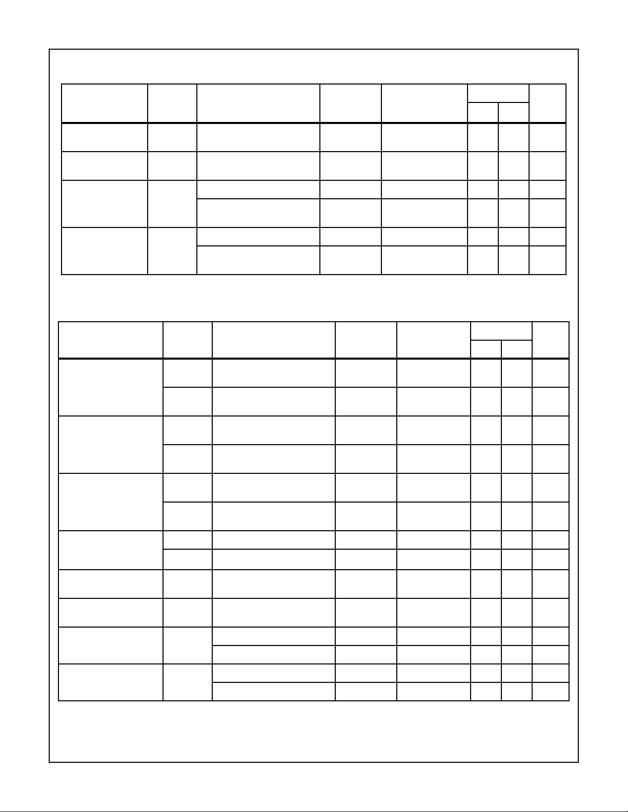
TABLE 5. HS-302RH/303RH/384RH/390RH/883S DC POST BURN-IN DELTA ELECTRICAL CHARACTERISTICS
Guaranteed, Per Mil-Std-883. Unless Otherwise Specified: V- = -15V, V+ = +15V, VAH = +4.0V, VAL = 0.8V (Continued)
PARAMETER SYMBOL CONDITIONS
GROUP A
SUB-
GROUPS TEMPERATURE
LIMITS
UNITSMIN MAX
Low Level Input
Address Current
High Level Input
Address Current
Positive Supply
Current
Negative Supply
Current
TABLE 5. HS-306RH/307RH/883S DC POST BURN-IN DELTA ELECTRICAL CHARACTERISTICS
Guaranteed, Per Mil-Std-883. Unless Otherwise Specified: V- = -15V, V+ = +15V, VAH = +11.0V, VAL = 3.5V
PARAMETER SYMBOL CONDITIONS
“Switch On” Resistance +RDS VD = 10V, IS = -10mA,
Leakage Current Into the
Source Terminal of an
“Off” Switch
IAL All Channels VA = 0.8V 1 +25oC -100 100 nA
IAH All Channels VA = 4.0V 1 +25oC -100 100 nA
I(+) All Channels VA = 0.8V 1 +25oC-11µA
VA1 = 0V, VA2 = 4.0V and
VA1 = 4.0V, VA2 = 0V
I(-) All Channels VA = 0.8V 1 +25oC-11µA
VA1 = 0V, VA2 = 4.0V and
VA1 = 4.0V, VA2 = 0V
S1/S2/S3/S4
-RDS VD = -10V, IS = 10mA,
S1/S2/S3/S4
+IS(OFF) VS = +14V, VD = -14V,
S1/S2/S3/S4
-IS(OFF) VS = -14V, VD = +14V,
S1/S2/S3/S4
1 +25oC -0.1 0.1 mA
1 +25oC-11µA
GROUP A
SUBGROUPS TEMPERATURE
1 +25oC-55Ω
1 +25oC-55Ω
1 +25oC-22nA
1 +25oC-22nA
LIMITS
UNITSMIN MAX
Leakage Current into the
Drain Terminal of an “Off”
Switch
Leakage Current from an
“On” Driver Into the Switch
(Drain & Source)
Low Level Input Address
Current
High Level Input Address
Current
Positive Supply Current I(+) All Channels VA = 0V 1 +25oC-11µA
Negative Supply Current I(-) All Channels VA = 0V 1 +25oC-11µA
+ID(OFF) VS = -14V, VD = +14V,
S1/S2/S3/S4
-ID(OFF) VS = +14V, VD = -14V,
S1/S2/S3/S4
+ID(ON) VS = VD = +14V, S1/S2/S3/S4 1 +25oC-22nA
-ID(ON) VS = VD = -14V, S1/S2/S3/S4 1 +25oC-22nA
IAL All Channels VA = 3.5V 1 +25oC -100 100 nA
IAH All Channels VA = 11V 1 +25oC -100 100 nA
All Channels VA = 15V 1 +25oC-11µA
All Channels VA = 15V 1 +25oC-11µA
1 +25oC-22nA
1 +25oC-22nA
Spec Number 518526
9
Page 10
Specifications HS-3XXRH/883S
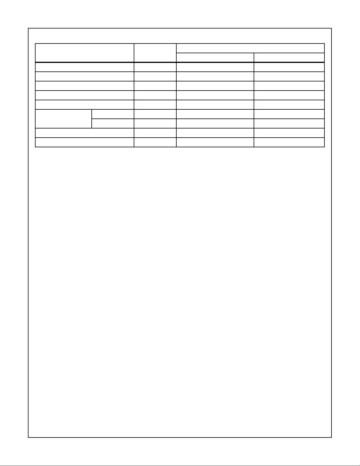
TABLE 6. APPLICABLE SUBGROUPS
GROUP A SUBGROUPS
CONFORMANCE GROUPS METHOD
Initial Test 100%/5004 1, 7, 9 1, (Note 2)
Interim Test 100%/5004 1, 7, 9, Deltas 1, Deltas, (Note 2)
PDA 100%/5004 1, 7, Deltas
Final Test 100%/5004 2, 3, 8A, 8B, 10, 11
Group A (Note 1) Sample/5005 1, 2, 3, 7, 8A, 8B, 9, 10, 11
Group B Subgroup B-5 Sample/5005 1, 2, 3, 7, 8A, 8B, 9, 10, 11, Deltas 1, 2, 3, Deltas, (Note 2)
Subgroup B-6 Sample/5005 1, 7, 9
Group D Sample/5005 1, 7, 9
Group E, Subgroup 2 Sample/5005 1, 7
NOTES:
1. Alternate Group A testing in accordance with Method 5005 of MIL-STD-883 may be exercised.
2. Table 5 parameters on.y.
TESTED RECORDED
10
Spec Number 518526
Page 11

HS-302RH/303RH/306RH/307RH/384RH/390RH/883S
Intersil Space Level Product Flow
Wafer Lot Acceptance (All Lots) Method 5007
(Includes SEM)
GAMMA Radiation Verification (Each Wafer) Method 1019,
4 Samples/Wafer, 0 Rejects
100% Nondestructive Bond Pull, Method 2023
Sample - Wire Bond Pull Monitor, Method 2011
Sample - Die Shear Monitor, Method 2019 or 2027
100% Internal Visual Inspection, Method 2010, Condition A
100% Temperature Cycle, Method 1010, Condition C,
10 Cycles
100% Constant Acceleration, Method 2001, Condition per
Method 5004
100% PIND, Method 2020, Condition A
100% External Visual
100% Serialization
100% Initial Electrical Test (T0)
100% Static Burn-In 1, Condition A or B, 72hrs. min.,
NOTES:
1. Failures from subgroup 1, 7 and deltas are used for calculating PDA. The maximum allowable PDA = 5% with no more than 3% of the
2. Radiographic (X-Ray) inspection may be performed at any point after serialization as allowed by Method 5004.
3. Alternate Group A testing may be performed as allowed by MIL-STD-883, Method 5005.
4. Data Package Contents:
o
+125
C min.
failures from subgroup 7.
• Cover Sheet (Intersil Name and/or Logo, P.O. Number, Customer Part Number, Lot Date Code, Intersil Part Number, Lot Number, Quantity).
• Wafer Lot Acceptance Report (Method 5007). Includes reproductions of SEM photos with percent of step coverage.
• GAMMA Radiation Report. Contains Cover page, disposition, Rad Dose, Lot Number, Test Package used, Specification Numbers, Test
equipment, etc. Radiation Read and Record data on file at Intersil.
• X-Ray report and film. Includes penetrometer measurements.
• Screening, Electrical, and Group A attributes (Screening attributes begin after package seal).
• Lot Serial Number Sheet (Good units serial number and lot number).
• Variables Data (All Delta operations). Data is identified by serial number.Data header includes lot number and date of test. (See Table6)
• Group B and D attributes and/or Generic data.
• The Certificate of Conformance is a part of the shipping invoice and is not part of the Data Book. The Certificate of Conformance is signed
by an authorized Quality Representative.
100% Interim Electrical Test (T1)
100% Delta Calculation (T0-T1)
100% PDA, Method 5004 (Note 1)
100% Dynamic Burn-In, Condition D, 240 hrs., +125
Equivalent, Method 1015
100% Interim Electrical Test (T2)
100% Delta Calculation (T0-T2)
100% PDA, Method 5004 (Note 1)
100% Final Electrical Test
100% Fine/Gross Leak, Method 1014
100% Radiographic, Method 2012 (Note 2)
100% External Visual, Method 2009
Sample - Group A, Method 5005 (Note 3)
Sample - Group B, Method 5005
Sample - Group D, Method 5005
100% Data Package Generation (Note 4)
o
Cor
11
Spec Number 518526
Page 12
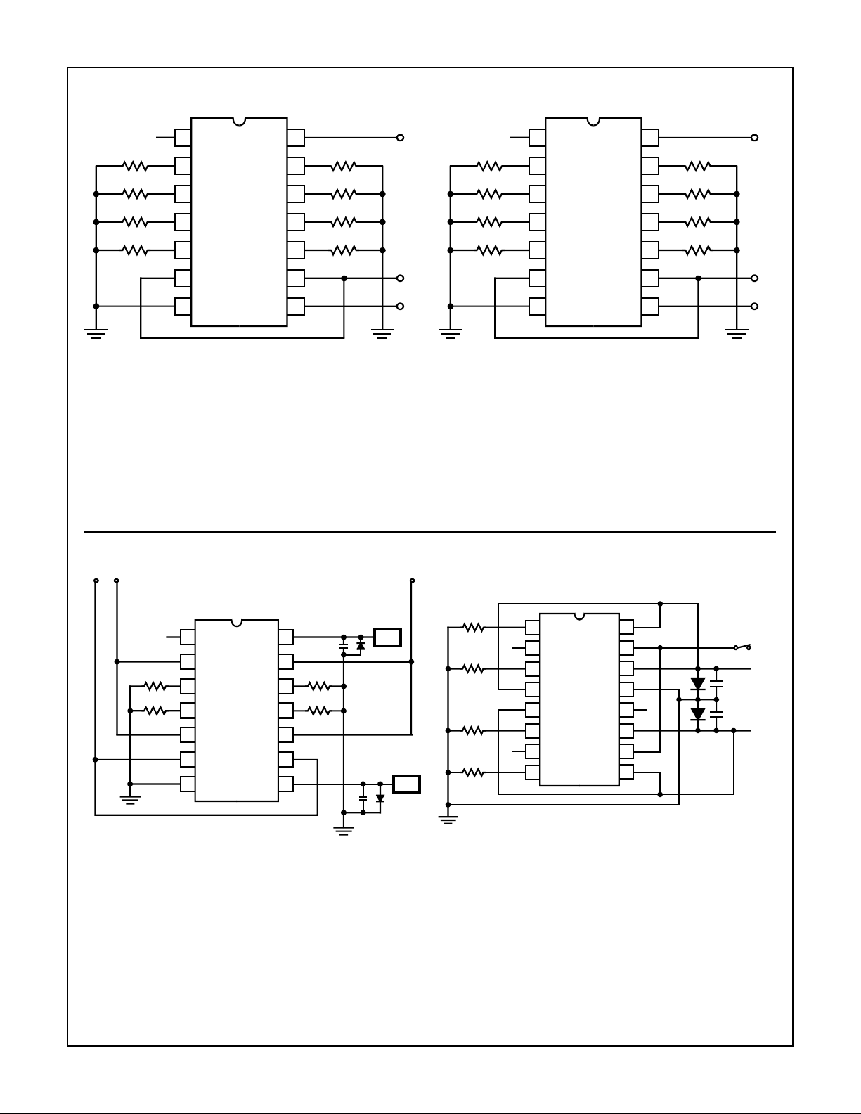
Irradiation Circuits
HS-302RH/303RH/306RH/307RH/384RH/390RH/883S
NC
1
R1
S3
2
R2
D3
3
R3
D1
4
R4 R5
S1
5
IN1
6
GND
7
V+
14
R8
S4
13
R7
D4
12
R6
D2
11
S2
10
IN2
9
V-
8
HS-302RH/303RH/883S
HS-384RH/390RH/883S
NOTES:
1. R1 - R8 = 10kΩ± 5%, 1/4W
2. V1 = +15V ± 10%
3. V2 = -15V ± 10%
4. V3 = +5V ± 10%
5. All irradiation testing is performed in the 14 pin package.
V1
V3
V2
NC
1
R1
S3
2
R2
D3
3
R3
D1
4
R4 R5
S1
5
IN1
6
GND
7
14
13
12
11
10
9
8
HS-306RH/307RH/883S
NOTES:
1. R1 - R8 = 10kΩ± 5%, 1/4W
2. V1 = +15V ± 10%
3. V2 = -15V ± 10%
4. V3 = +12V ± 10%
5. All irradiation testing is performed in the 14 pin package.
V+
S4
D4
D2
S2
IN2
V-
V1
R8
R7
R6
V3
V2
Burn-In Circuits
V-VA V+
NC
1
2
R
3
R
4
5
6
7
14
13
12
11
10
9
8
C
R
R
STATIC CONFIGURATION
HS-302RH/303RH/306RH/307RH/883S
NOTES:
1. R = 10KΩ± 5%, 1/4W (4 per position)
2. C = 0.01µF minimum (per position) or 0.1µF minimum per row
3. D = IN4002 (or equivalent)
4. +V = +15.5V ± 0.5V, -V = -15.5V ± 0.5V
5. VA = +15.5V ± 0.5V for 306RH/307RH
6. VA = +5.5V ± 0.5V for 302RH/303RH
V+
D
C
D
R
R
R
R
V-
1
2
3
4
5
6
7
8
16
15
14
13
12
11
10
9
D
D
VA
-V
C
C
+V
STATIC CONFIGURATION
HS-384RH/390RH/883S
NOTES:
1. R = 10KΩ± 5%, 1/4W (4 per position)
2. C = 0.01µF minimum (per position) or 0.1µF minimum per row
3. D = IN4002 (or equivalent)
4. +V = +15.5V ± 0.5V, -V = -15.5V ± 0.5V
5. VA = +5.5V ± 0.5V
12
Spec Number 518526
Page 13
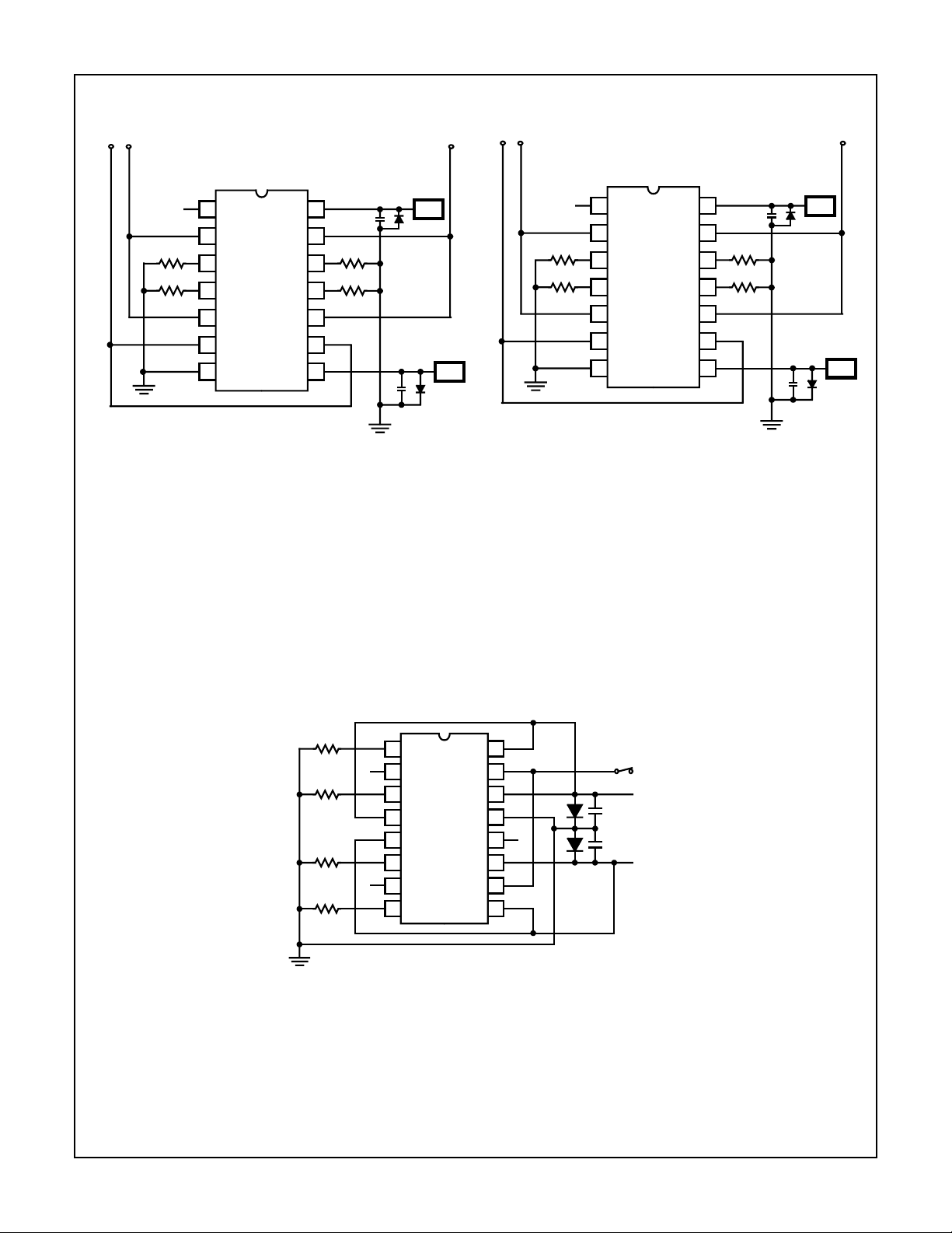
HS-302RH/303RH/306RH/307RH/384RH/390RH/883S
Burn-In Circuits
V-FV+
NC
R
R
NOTES:
1. R = 10KΩ± 5%, 1/4W (4 per position)
2. C = 0.01µF minimum (per position) or 0.1µF minimum per row
3. D = IN4002 (or equivalent)
4. F = 100kHz square wave, 50% duty cycle,
VL = 0.8V max., VH = 5.5V ± 0.5V
5. +V = +15.5V ± 0.5V, -V = -15.5V ± 0.5V
(Continued)
1
2
3
4
5
6
7
14
13
R
12
R
11
10
9
8
DYNAMIC CONFIGURATION
HS-302RH/303RH/883S
V-FV+
1
C
V+
D
C
V-
D
NC
2
R
3
R
4
5
6
7
14
13
12
11
10
9
8
DYNAMIC CONFIGURATION
HS-306RH/307RH/883S
NOTES:
1. R = 10KΩ± 5%, 1/4W (4 per position)
2. C = 0.01µF minimum (per position) or 0.1µF minimum per row
3. D = IN4002 (or equivalent)
4. F = 100kHz square wave, 50% duty cycle,
VL = 0.8V max., VH = 14V ± 1V
5. +V = +15.5V ± 0.5V, -V = -15.5V ± 0.5V
C
R
R
V+
D
C
V-
D
R
R
R
R
1
2
3
4
5
6
7
8
DYNAMIC CONFIGURATION
HS-384RH/390RH/883S
NOTES:
1. R = 10KΩ± 5%, 1/4W (4 per position)
2. C = 0.01µF minimum (per position) or 0.1µF minimum per row
3. D = IN4002 (or equivalent)
4. F = 100kHz square wave, 50% duty cycle,
VL = 0.8V max., VH = +5.5V ±0.5V
5. +V = +15.5V ± 0.5V, -V = -15.5V ± 0.5V
13
16
15
14
13
12
11
10
9
D
D
F
-V
C
C
+V
Spec Number 518526
Page 14
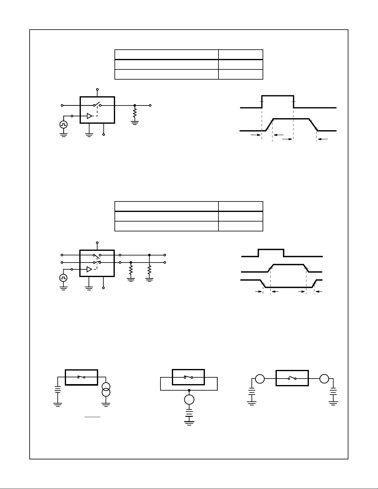
Test Circuits
HS-302RH/303RH/306RH/307RH/384RH/390RH/883S
SWITCH TYPE VINH
HS-302RH/303RH/384RH/390RH/883S 4V
HS-306RH/307RH/883S 15V
VS = +3V
LOGIC
INPUT
VS1 = +3V
VS2 = +3V
LOGIC
INPUT
GND
GND
V+
+15V
VO
SWITCH
OUTPUT
SWITCH OUTPUT
V-
-15V
RL
300Ω
FIGURE 1. SWITCHING TEST CIRCUIT (tON, tOFF)
SWITCH TYPE VINH
HS-303RH/390RH/883S 5V
HS-307RH/883S 15V
V+
+15V
V-
-15V
D1
D2
RL2
RL1
OUT 1
OUT 2
SWITCH OUTPUT
LOGIC INPUT
0V
VS
0V
LOGIC INPUT
LOGIC “1” = SWITCH ON
VINH
50% 50%
90%
tON
LOGIC “1” =
SWITCH ON
VINH
0V
0V
0V
50%
tBBM tBBM
tOFF
RL1 = RL2 = 300Ω
50%50%
10%
50%
OUT 1
OUT 2
VBVA
±10V
RON =
VB - VA
± 10mA
±
FIGURE 3. ON RESISTANCE TEST
CIRCUIT (RON)
FIGURE 2. BREAK-BEFORE-MAKE TEST CIRCUIT (tBBM)
SD
10mA
ID(ON)
A
±14V
FIGURE 4. ON LEAKAGE CURRENT
TEST CIRCUIT (IDON)
14
ID(OFF)
A
±
14V
SD
IS(OFF)
A
±14V
FIGURE 5. OFF LEAKAGE CURRENT
TEST CIRCUIT (ISOFF,
IDOFF)
Spec Number 518526
Page 15
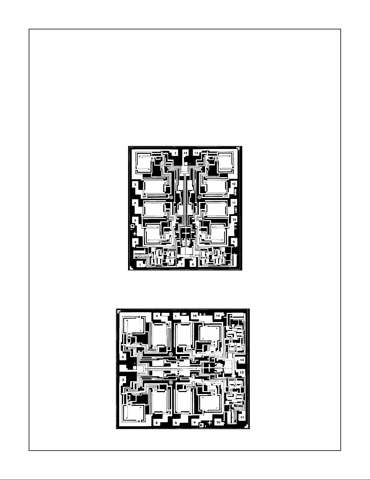
HS-302RH/303RH/306RH/307RH/384RH/390RH/883S
Metallization Topology
DIE DIMENSIONS:
Die Size: 2130 x 1930µm
Die Thickness: 11 ±1 mils
METALLIZATION:
Type: Al, 12.5k
Å ± 2kÅ
Back: Gold
GLASSIVATION:
Type: SiO
2
Thickness: 8kű 1kÅ
Metallization Mask Layout
WORST CASE CURRENT DENSITY: 1.732e05 A/cm
SUBSTRATE POTENTIAL: Unbiased
PROCESS: DI Linear Metal Gate CMOS
HS-302RH/303RH/306RH/307RH/883S
V+
S3
S4
2
S3
D3
D1
S1
IN1
NC
HS-384RH/390RH/883S
D3
D1
GND
D4
D2
S2
IN2
V-
S1
IN1
V-
S4
D4
D2
15
S2
GND
V+
IN2
Spec Number 518526
Page 16

HS-302RH/303RH/306RH/307RH/384RH/390RH/883S
All Intersil semiconductor products are manufactured, assembled and tested under ISO9000 quality systems certification.
Intersil semiconductor products are sold by description only. Intersil Corporation reserves the right to make changes in circuit design and/or specifications at any time without notice. Accordingly, the reader is cautioned to verify that data sheets are current before placing orders. Information furnished by Intersil is believed to be accurate and
reliable. However, no responsibility is assumed by Intersil or its subsidiaries for its use; nor for any infringements of patents or other rights of third parties which may result
from its use. No license is granted by implication or otherwise under any patent or patent rights of Intersil or its subsidiaries.
For information regarding Intersil Corporation and its products, see web site http://www.intersil.com
Sales Office Headquarters
NORTH AMERICA
Intersil Corporation
P. O. Box 883, Mail Stop 53-204
Melbourne, FL 32902
TEL: (407) 724-7000
FAX: (407) 724-7240
EUROPE
Intersil SA
Mercure Center
100, Rue de la Fusee
1130 Brussels, Belgium
TEL: (32) 2.724.2111
FAX: (32) 2.724.22.05
ASIA
Intersil (Taiwan) Ltd.
7F-6, No. 101 Fu Hsing North Road
Taipei, Taiwan
Republic of China
TEL: (886) 2 2716 9310
FAX: (886) 2 2715 3029
Spec Number
16
 Loading...