

Page 1
MICROWAVE CORPORATION
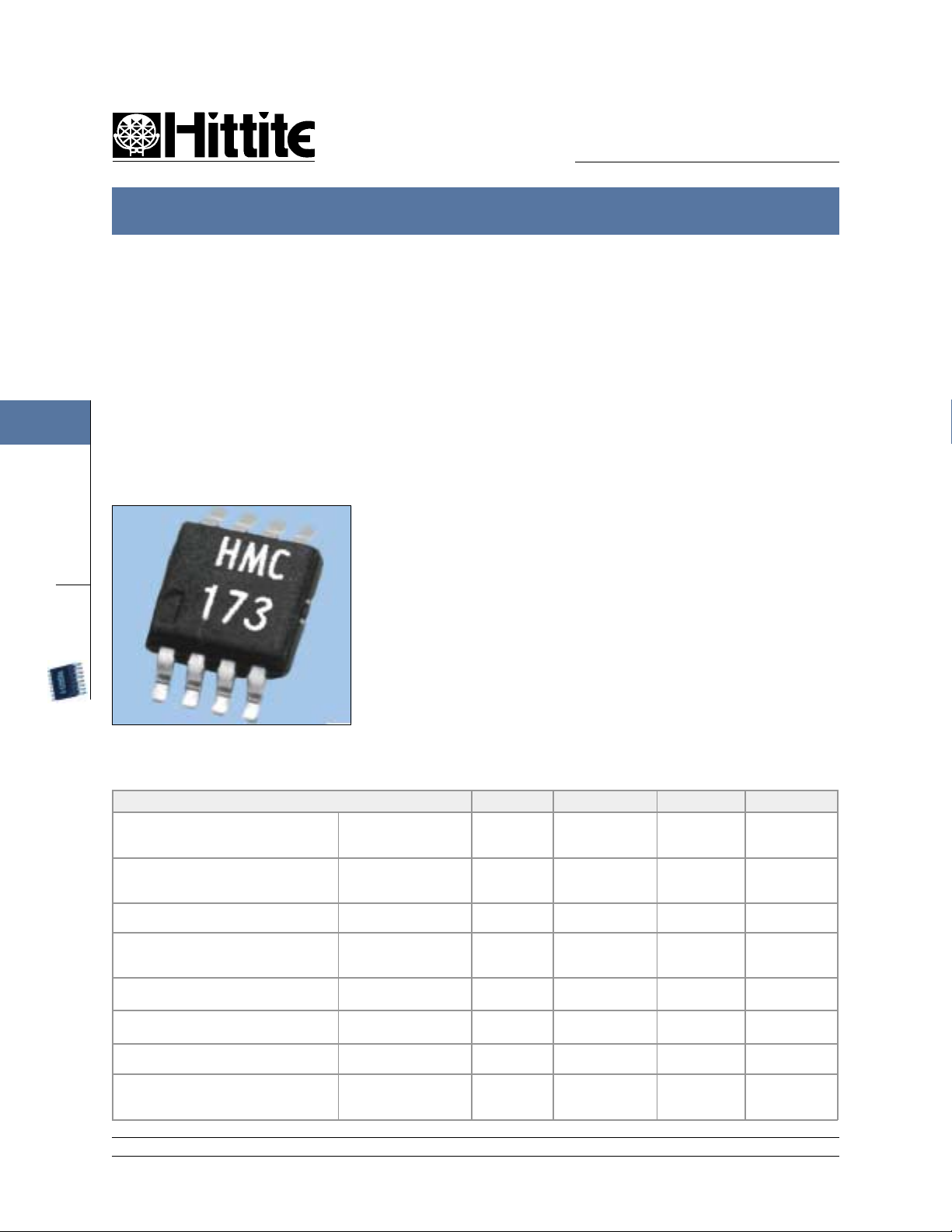
HMC173MS8
GaAs MMIC VOLTAGE VARIABLE ATTENUATOR 800-2000 MHz
FEBRUARY 2001
2
ATTENUATORS
SMT
Features
SINGLE POSITIVE VOLTAGE CONTROL: 0 to +3V
HIGH ATTENUATION RANGE: >50 dB @ 0.9 GHz
HIGH P1dB COMPRESSION POINT: +16 dBm
ULTRA SMALL PACKAGE: MSOP
General Description
The HMC173MS8 is a miniature absorptive voltage variable attenuator in an 8lead MSOP package. The device operates with a positive supply voltage, and a
positive control voltage. Unique features
include a high dynamic attenuation range,
and excellent power handling performance
through all attenuation states. The
HMC173MS8 is ideal for operation in wireless applications between 800 MHz and
1600 MHz. 1.7 to 2.0 GHz operation is
possible, with a reduced maximum attenuation of 30 dB and increased VSWR. The
HMC173MS8 can be used with an external driver circuit for improved linearity of
attenuation.
Guaranteed Performance V
Parameter Min Typical Max Units
Insertion Loss (Min.Atten.)
(V
=0.0Vdc)
CTL
Attenuation Range
(V
=0to+3V)
CTL
Flatness
(Peak to Peak)
Return Loss
(V
=0to+3V)
CTL
Input Power for 0.1 dB Compression
(825 MHz)
Input Power for 1.0 dB Compression
(825 MHz)
Input Third Order Intercept
825 MHz, two tones @ +5.0 dBm
SwitchingCharacteristics
t
RISE,tFALL
t
ON,tOFF
12 Elizabeth Drive, Chelmsford, MA 01824 Phone: 978-250-3343 Fax: 978-250-3373 Web Site: www.hittite.com
(10/90% R F )
(50% CTL to 10/90%RF )
2 - 26
800-1000 MHz
1000-1600 MHz
1600-2000 MHz
800-1000 MHz
1000-1600 MHz
1600-2000 MHz
800-1000 MHz
1000-1600 MHz
800-1000 MHz
1000-1600 MHz
1600-2000 MHz
Min Atten.
Atten.>2.0
Min Atten.
Atten.>2.0
Min Atten.
Atten.>2.0
800-2000 MHz 1.0
= +4.0 Vdc, 50 Ohm System, -40 to +85°C
dd
45
27
25
10
30
15
21
1.8
2.6
3.2
52
32
30
±0.15
±0.25
6
5
5
12
8
7
19
9
25
16
37
21
1.2
2.3
3.1
3.7
dB
dB
dB
dB
dB
dB
dB
dB
dB
dB
dB
dBm
dBm
dBm
dBm
dBm
dBm
µS
µS
Page 2
HMC173MS8
MICROWAVE CORPORATION
HMC173MS8 VOLTAGE VARIABLE ATTENUATOR 800-2000 MHz
FEBRUARY 2001
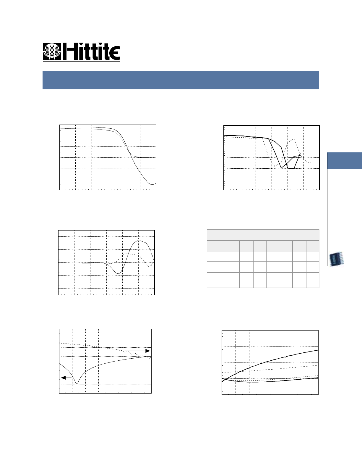
Attenuation vs. Control Voltage
@900 and 1900 MHz
0
-10
-20
-30
-40
ATTENUATION (dB)
-50
-60
0 0.5 1 1.5 2 2.5 3
CONTROL VOLTAGE (V)
825
1900 MHz
MHz
Attenuation vs. Temperature
Normalized to +25°C @825 MHz
10
8
6
4
2
0
-2
-4
-6
-8
NORMALIZED ATTENUATION (dB)
-10
0 0.5 1 1.5 2 2.5 3
CONTROL VOLTAGE (V)
-40C
+85C
Broadband Attenuation and
Insertion Loss
0
-10
-20
-30
-40
-50
ATTENUATION (dB)
-60
-70
0.6 0.8 1 1.2 1.4 1.6 1.8 2
FREQUENCY (GHz)
0
-1
-2
-3
-4
-5
INSERTION LOSS (dB)
-6
-7
Input IP3 vs. Control Voltage
@825 MHz
40
35
30
25
20
15
825 MHz INPUT IP3 (dBm)
10
0 0.5 1 1.5 2 2.5 3
+85C
CONTROL VOLTAGE (V)
-40C
+25C
Input P1dB Compression
@825 MHz
Input Power For 1 dB Compression Point
Test Condition
(825MHz)
Min.Attenuation 0.0 +4.0 26 24 25 dBm
Max.Attenuation +3.0 +4.0 16.5 15 23 dBm
Worst Case
P1dB @
Typical V
CTL
V
Vdd
CTL
(Vdc)
+1.8 +4.0 16.5 15.5 14 dBm
+25C +85C -40C Units
(Vdc)
Broadband Return Loss vs.
Control Voltage
0
-5
V
0
-10
2V
-15
RETURN LOSS (dB)
-20
0.6 0.8 1 1.2 1.4 1.6 1.8 2
FREQUENCY (GHz)
2.25V
3V
2
ATTENUATORS
SMT
S - Parameter data is available On-Line at www.hittite.com
12 Elizabeth Drive, Chelmsford, MA 01824 Phone: 978-250-3343 Fax: 978-250-3373 Web Site: www.hittite.com
2 - 27
Page 3

HMC173MS8
MICROWAVE CORPORATION
HMC173MS8 VOLTAGE VARIABLE ATTENUATOR 800-2000 MHz
FEBRUARY 2001
Typical Performance for 800-1000 MHz Applications
2
ATTENUATORS
SMT
Attenuation vs. Control Voltage
825 MHz
0
-10
-20
-30
-40
ATTENUATION (dB)
-50
-60
0 0.5 1 1.5 2 2.5 3
+85C
+25C
CONTROL VOLTAGE (V)
-40C
Return Loss vs. Control Voltage
825 MHz
0
-2
-4
-6
-8
-10
-12
-14
RETURN LOSS (dB)
-16
-18
-20
0 0.5 1 1.5 2 2.5 3
CONTROL VOLTAGE (V)
-40C and +85C
+25C
Typical Performance for 1800-1900 MHz Applications
Attenuation vs. Control Voltage
1900 MHz
0
-5
-10
-15
-20
-25
ATTENUATION (dB)
-30
-35
0 0.5 1 1.5 2 2.5 3
-40C
+25C
CONTROL VOLTAGE (V)
+85C
Return Loss vs. Control Voltage
1900 MHz
0
-2
-4
-6
-8
-10
-12
-14
RETURN LOSS (dB)
-16
-18
-20
0 0.5 1 1.5 2 2.5 3
CONTROL VOLTAGE (V)
+25C
+85C
-40C
12 Elizabeth Drive, Chelmsford, MA 01824 Phone: 978-250-3343 Fax: 978-250-3373 Web Site: www.hittite.com
2 - 28
Page 4

HMC173MS8
MICROWAVE CORPORATION
HMC173MS8 VOLTAGE VARIABLE ATTENUATOR 800-2000 MHz
FEBRUARY 2001
Functional Diagram
RF2 V
GND N/C
PIN 1
* NOTE: DC blocking capacitors are required for each RF port. Capacitor value
determines lowest frequency of operation.
V
dd
CTL
N/CGNDRF1
Outline Drawing
Gnd
Vdd
RF2
N/C
0.116/ 0.120
(2.95/ 3.05)
Control and Bias Voltages
V
LTC
ddV001+@cdV1.0-/+cdV0.4+ µA
001-@cdV0.3+ot0 µ 001+otA µA
Absolute Maximum Ratings
V
CTL
Vdd +8 Vdc
MaximumInput Power
Vdd = +4.0 Vdc
Storage Temperature -65 to +150 deg.C
Operating Temperature -40 to +85 deg.C
-0.2 Vdc to Vdd
+29 dBm
+21 dBm
LOT NUMBER
Min Attenuation
Att.> 2 dB
2
ATTENUATORS
SMT
0.116/ 0.120
(2.95/ 3.05)
PIN 1
0.038/ 0.042
(0.96/ 1.07)
12 Elizabeth Drive, Chelmsford, MA 01824 Phone: 978-250-3343 Fax: 978-250-3373 Web Site: www.hittite.com
0.0256 TYP
(0.65)
1. MATERIAL:
A) PACKAGE BODY - LOW STRESS INJECTION - MOLDED PLASTIC, SILICA & SILICONE IMPREGNATED.
B) LEADFRAME MATERIAL: COPPER ALLOY
2. PLATING: LEAD - TIN SOLDER PLATE
3. DIMENSIONS ARE IN INCHES (MILLIMETERS), UNLESS OTHERWISE SPECIFIED TOL. ARE ±0.005(±0.13)
4. TAPE AND REEL SHIPMENT PACKAGING AVAILABLE, SEE PAGE 10 - 1
HMC
173
RF1
Gnd
CTL
V
0.188/ 0.196
(4.78/ 4.98)
N/C
0.032/ 0.036
0.012 TYP
(0.30)
(0.81/ 0.91)
0 to 5 deg
XXXX
YYWW
0.021 MIN TYP
(0.53)
DATE CODE
YY= YEAR
WW= WEEK
PIN 1 (REF)
0.005/ 0.007
(0.13/ 0.18)
2 - 29
Page 5

HMC173MS8
MICROWAVE CORPORATION
HMC173MS8 VOLTAGE VARIABLE ATTENUATOR 800-2000 MHz
FEBRUARY 2001
Attenuation Linearizing Control Circuit For The
HMC173MS8 Voltage Variable Attenuator
A driver circuit to improve the attenuation linearity of the HMC173MS8 can be implemented with a simple op-amp
configuration. A breakpoint linearization circuit will scale the voltage supplied to the control line of the HMC173MS8,
so that a more linear attenuation vs. control voltage slope can be achieved. A -5V and +5V supply is required.
2
ATTENUATORS
SMT
Diode and resistor values which define the op-amp gain, and breakpoint were selected to optimize a measured
production lot of attenuators at 825 MHz. R7 may be varied to optimize the performance of any given attenuator. If the
input voltage to the linearizing circuit will not drop below 1.0V, then R9 and D2 may be omitted, and this will greatly reduce
the overall power consumption of the driver circuit.
The linearizing circuit has been optimized for 825 MHz attenuation applications. A similar approach may be used at other
frequencies by adjusting RI - R9 resistor values.
Required Parts List Schematic
Part Description Manufacturer
AD822 Op-Amp Analog Devices
R1 10K ohms Panasonic
R2 200K ohms Panasonic
R3 7.5K ohms Panasonic
R4 39K ohms Panasonic
R5 220K ohms Panasonic
R6 91K ohms Panasonic
R7 910 ohms Panasonic
R8 51 ohms Panasonic
R9 100 ohms Panasonic
D1, D2 LL4148 D-35 Di gi key
Return Loss vs. Control Voltage
@ 825 MHz
-12
-13
-14
-15
-16
With
Linearizer
-17
RETURN LOSS (dB)
-18
-19
0.5 1 1.5 2 2.5 3
CONTROL VOLTAGE (Vdc)
Without
Linearizer
V
CTL IN
0
R6
R5
R8
0
R7
+5
-5V
3
7
U3
+
2
D1
R4
AD820/AD
_
R1
-5V
6
V+
V-
4
R2
R3
Attenuation vs. Control Voltage
@ 825 MHz
0
-10
-20
-30
-40
ATTENUATION (dB)
-50
-60
0123
With
Linearizer
CONTROL VOLTAGE (Vdc)
R9
D2
+5V
V
CTL OUT
Without
Linearizer
12 Elizabeth Drive, Chelmsford, MA 01824 Phone: 978-250-3343 Fax: 978-250-3373 Web Site: www.hittite.com
2 - 30
Page 6

HMC173MS8
MICROWAVE CORPORATION
HMC173MS8 VOLTAGE VARIABLE ATTENUATOR 800-2000 MHz
Evaluation Circuit Board
FEBRUARY 2001
2
ATTENUATORS
The circuit board used in the final application should use RF circuit design techniques. Signal lines should have
50 ohm impedance while the package ground leads should be connected directly to the ground plane similar to
that shown below. A sufficient number of VIA holes should be used to connect the top and bottom ground planes.
The evaluation circuit board as shown is available from Hittite upon request.
Evaluation Circuit Board Layout Design Details
Layout Technique Grounded Co-Planar Waveguide (GCPW)
Material FR4
Dielectric Thickness 0.028" (0.71 mm)
50 Ohm Line Width 0.037" (0.94 mm)
Gap to Ground Edge 0.010" (0.25 mm)
Ground VIA Hole Diameter 0.014" (0.36 mm)
Connectors SMA-F ( EF - Johnson P/N 142-0701-806)
SMT
12 Elizabeth Drive, Chelmsford, MA 01824 Phone: 978-250-3343 Fax: 978-250-3373 Web Site: www.hittite.com
2 - 31
 Loading...