

Page 1

HD74ALVC162834A
18-bit Universal Bus Driver with 3-state Outputs
and Inverted Latch Enable
ADE-205-293A (Z)
2nd. Edition
November 1999
Description
The HD74ALVC162834A is an 18-bit universal bus driver designed for 2.3 V to 3.6 V VCC operation.
Data flow from A to Y is controlled by the output enable (OE). The device operates in the transparent mode
when the latch enable (LE) is low. When LE is low, the A data is latched if the clock (CLK) input is held
at a high or low logic level. If the LE is high, the A data is stored in the latch/flip flop on the low to high
transition of CLK. When OE is high, the outputs are in the high impedance state.
To ensure the high impedance state during power up or power down, OE should be tied to VCC through a
pullup registor; the minimum value of the registor is determined by the current sinking capability of the
driver.
All outputs, which are designed to sink up to 12 mA, include series dumping resistors to reduce overshoot
and undershoot.
Features
• Supports PC133 and meets “PC SDRAM registered DIMM specification, Rev. 1.1”
• VCC = 2.3 V to 3.6 V
• Typical VOL ground bounce < 0.8 V (@VCC = 3.3 V, Ta = 25°C)
• Typical VOH undershoot > 2.0 V (@VCC = 3.3 V, Ta = 25°C)
• High output current ±12 mA (@VCC = 3.0 V)
• All outputs have series dumping resistors, so no external resistors are required
• tpd (CLK to Y) = 3.5 ns (Max) (@VCC = 3.3±0.3 V, CL = 50 pF, Ta = 0 to 85°C)
• tpd (CLK to Y) = 2.5 ns (Max) (@VCC = 3.3±0.3 V, CL = 30 pF, Ta = 0 to 85°C)
Page 2

HD74ALVC162834A
Function Table
Inputs
OE LE CLK A Output Y
HXXX Z
LLXLL
LLXHH
LH↑ LL
LH↑ HH
L H L or H X Y
H : High level
L : Low level
X : Immaterial
Z : High impedance
↑ : Low to high transition
Note: 1. Output level before the indicated steady-state input conditions were established.
*1
0
2
Page 3
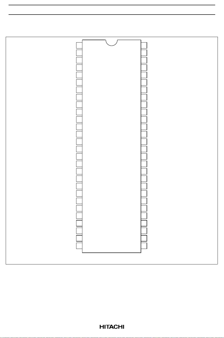
Pin Arrangement
HD74ALVC162834A
NC
NC
Y1
GND
Y2
Y3
V
CC
Y4
Y5
Y6
GND
Y7
Y8
Y9
Y10
Y11
Y12
GND
Y13
Y14
Y15
V
CC
Y16
Y17
GND
Y18
OE
LE
10
11
12
13
14
15
16
17
18
19
20
21
22
23
24
25
26
27
28
56
55
54
53
52
51
50
49
48
47
46
45
44
43
42
41
40
39
38
37
36
35
34
33
32
31
30
29
GND
NC
A1
GND
A2
A3
V
CC
A4
A5
A6
GND
A7
A8
A9
A10
A11
A12
GND
A13
A14
A15
V
CC
A16
A17
GND
A18
CLK
GND
1
2
3
4
5
6
7
8
9
(Top view)
3
Page 4
HD74ALVC162834A
Absolute Maximum Ratings
Item Symbol Ratings Unit Conditions
Supply voltage range V
Input voltage range
Output voltage range
*1
*1, 2
Input clamp current I
Output clamp current I
Continuous output current I
VCC, GND current / pin ICC or I
Maximum power dissipation
at Ta = 55°C (in still air)
*3
CC
V
I
V
O
IK
OK
O
GND
P
T
Storage temperature range Tstg –65 to 150 °C
Stresses beyond those listed under “absolute maximum ratings” may cause permanent damage to the
device. These are stress ratings only, and functional operation of the device at these or any other conditions
beyond those indicated under “recommended operating condition” is not implied. Exposure to absolutemaximum-rated conditions for extended periods may affect device reliability.
Notes: 1. The input and output negative-voltage ratings may be exceeded if the input and output clamp
current ratings are observed.
2. The input and output positive-voltage ratings may be exceeded up to 4.6 V if the input and output
clamp-current ratings are observed.
3. The maximum power dissipation is calculated using a junction temperature of 150°C and board
trace length of 750 mils.
–0.5 to 4.6 V
–0.5 to 4.6 V
–0.5 to VCC+0.5 V
–50 mA VI < 0
±50 mA VO < 0 or VO > V
±50 mA VO = 0 to V
CC
±100 mA
1 W TSSOP
CC
Recommended Operating Conditions
Item Symbol Min Max Unit Conditions
Supply voltage V
Input voltage V
Output voltage V
High-level output current I
Low-level output current I
CC
I
O
OH
OL
Input transition rise or fall rate ∆t/∆v 0 10 ns/V
Operating free-air temperature Ta –40 85 °C
Note: Unused or floating control pins must be held high or low.
2.3 3.6 V
0VCCV
0VCCV
—–6mAV
—–8 V
= 2.3 V
CC
= 2.7 V
CC
— –12 VCC = 3.0 V
— 6 mA VCC = 2.3 V
—8 V
—12 V
= 2.7 V
CC
= 3.0 V
CC
4
Page 5
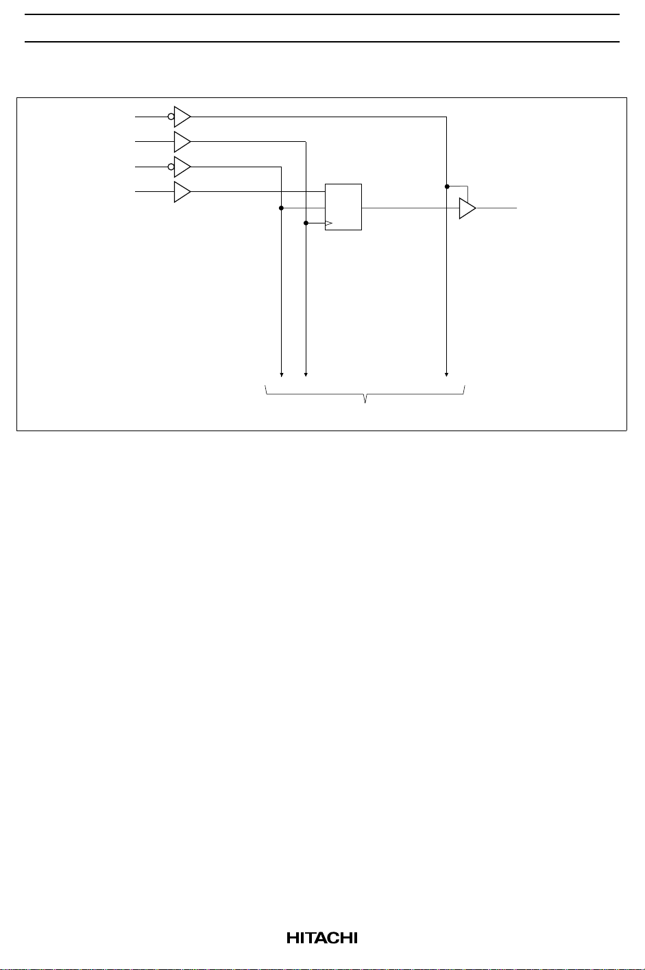
Logic Diagram
OE
CLK
LE
A1
HD74ALVC162834A
27
30
28
54
1D
C1
CLK
To seventeen other channels
3
Y1
5
Page 6

HD74ALVC162834A
Electrical Characteristics
Item Symbol V
Input voltage V
Output voltage V
Input current I
Off state output current I
Quiescent supply current I
V
V
∆I
IH
IL
OH
OL
IN
OZ
CC
CC
Ta = –40 to 85°C
(V) Min Max Unit Test Conditions
CC
2.3 to 2.7 1.7 — V
2.7 to 3.6 2.0 —
2.3 to 2.7 — 0.7 V
2.7 to 3.6 — 0.8
2.3 to 3.6 VCC–0.2 — V IOH = –100 µA
2.3 1.9 — IOH = –4 mA, VIH = 1.7 V
2.3 1.7 — IOH = –6 mA, VIH = 1.7 V
3.0 2.4 — IOH = –6 mA, VIH = 2.0 V
2.7 2.0 — IOH = –8 mA, VIH = 2.0 V
3.0 2.0 — IOH = –12 mA, VIH = 2.0 V
2.3 to 3.6 — 0.2 V IOL = 100 µA
2.3 — 0.4 IOL = 4 mA, VIL = 0.7 V
2.3 — 0.55 IOL = 6 mA, VIL = 0.7 V
3.0 — 0.55 IOL = 6 mA, VIL = 0.8 V
2.7 — 0.6 IOL = 8 mA, VIL = 0.8 V
3.0 — 0.8 IOL = 12 mA, VIL = 0.8 V
3.6 — ±5.0 µAVIN = VCC or GND
3.6 — ±10 µAV
= VCC or GND
OUT
3.6 — 40 µAVIN = VCC or GND
3.0 to 3.6 — 750 µA One input at (VCC–0.6)V,
other inputs at V
or GND
CC
6
Page 7

HD74ALVC162834A
Switching Characteristics (Ta = –40 to 85°C)
Item Symbol VCC (V) Min Typ Max Unit From (Input) To (Output)
Maximum clock f
max
frequency 2.7 150 — —
Propagation delay time t
Output enable time t
Output disable time t
Input capacitance C
Output capacitance C
PLH
t
PHL
ZH
t
ZL
HZ
t
LZ
IN
O
2.5±0.2 150 — — MHz
3.3±0.3 150 — —
2.5±0.2 1.0 — 5.0 ns A Y
2.7 — — 5.0
3.3±0.3 1.0 — 4.2
2.5±0.2 1.4 — 6.3 LE Y
2.7 — — 6.1
3.3±0.3 1.4 — 5.4
2.5±0.2 1.4 — 6.3 CLK Y
2.7 — — 6.1
3.3±0.3 1.4 — 5.4
2.5±0.2 1.4 — 6.3 ns OE Y
2.7 — — 6.5
3.3±0.3 1.1 — 5.5
2.5±0.2 1.0 — 4.7 ns OE Y
2.7 — — 4.9
3.3±0.3 1.3 — 4.5
3.3 3.3 4.0 4.5 pF Control inputs
3.3 3.0 6.0 9.0 Data inputs
3.3 3.0 7.0 9.0 pF Y ports
7
Page 8

HD74ALVC162834A
Switching Characteristics (Ta = –40 to 85°C) (cont)
Item Symbol VCC (V) Min Typ Max Unit From (Input)
Setup time t
Hold time t
Pulse width t
su
h
w
2.5±0.2 2.2 — — ns Data before CLK↑
2.7 2.1 — —
3.3±0.3 1.7 — —
2.5±0.2 1.2 — — Data before LE↑
2.7 1.6 — — CLK “H”
3.3±0.3 1.3 — —
2.5±0.2 1.4 — — Data before LE↑
2.7 1.5 — — CLK “L”
3.3±0.3 1.2 — —
2.5±0.2 0.6 — — ns Data after CLK↑
2.7 0.6 — —
3.3±0.3 0.7 — —
2.5±0.2 1.2 — — Data after LE↑
2.7 1.1 — — CLK “H” or “L”
3.3±0.3 1.1 — —
2.5±0.2 3.3 — — ns LE “L”
2.7 3.3 — —
3.3±0.3 3.3 — —
2.5±0.2 3.3 — — CLK “H” or “L”
2.7 3.3 — —
3.3±0.3 3.3 — —
Switching Characteristics (Ta = 0 to 85°C)
Item Symbol VCC (V) Min Typ Max Unit FROM
(Input)TO(Output)
Propagation delay time C
Setup time t
Hold time t
8
=50pF t
L
CL=30pF 3.3±0.3 0.7 — 2.5 CLK Y
PLH
su
h
, t
3.3±0.3 1.4 — 3.5 ns CLK Y
PHL
3.3±0.3 1.0 — — ns Data before CLK↑
3.3±0.3 0.6 — — ns Data after CLK↑
Page 9

HD74ALVC162834A
Operating Characteristics (Ta = 25°C)
Item Symbol VCC = 2.5±0.2 V VCC = 3.3±0.3 V Unit Test Conditions
Typ Typ
Power dissipation Outputs enable C
capacitance Outputs disable 5.0 6.0
pd
22.0 24.5 pF CL = 0, f = 10 MHz
9
Page 10

HD74ALVC162834A
Test Circuit
See under table
500 Ω
S1
OPEN
GND
*1
L
500 ΩC
Load Circuit for Outputs
Symbol
t / t
PLH PHL
t / t / t
su h w
t / t
ZH HZ
t / t
ZL LZ
C
Vcc=2.5±0.2V
2 × V 6.0 V
L
Note: 1. CL includes probe and jig capacitance.
Vcc=2.7V,
3.3±0.3V
OPEN
GND
OPEN
GND
CC
30 pF 50 pF
10
Page 11

Waveforms – 1
HD74ALVC162834A
Input
Output
Waveforms – 2
Timing Input
Data Input
10 %
t
rf
V
90 %
ref
90 %
t
V
ref
10 %
t
PLH
V
ref
t
r
t
PHL
V
ref
90 %
V
ref
10 %
t
su
V
ref
t
h
V
ref
V
IH
GND
V
OH
V
OL
V
IH
GND
V
IH
GND
Input
t
w
V
IH
V
ref
V
ref
GND
11
Page 12

HD74ALVC162834A
Waveforms – 3
t
r
90 %
V
ref
t
LZ
V
ref1
t
HZ
V
ref2
CC
Vcc=2.7V,
3.3±0.3V
V +0.3 V
OL
V –0.3 V
OH
TEST
V
IH
V
ref
V
ref1
V
ref2
V
OH1
V
OL1
Vcc=2.5±0.2V
V
CC
1/2 V 1.5 V
V +0.15 V
OL
V –0.15 V
OH
V
CC
GND
Output
Control
Waveform - A
Waveform - B
90 %
t
f
V
ref
10 % 10 %
t
ZL
V
ref
t
ZH
V
ref
Notes: 1. All input pulses are supplied by generators having the following characteristics :
PRR ≤ 10 MHz, Zo = 50 Ω, tr ≤ 2.0 ns, tf ≤ 2.0 ns. (VCC = 2.5±0.2 V)
PRR ≤ 10 MHz, Zo = 50 Ω, tr ≤ 2.5 ns, tf ≤ 2.5 ns. (VCC = 2.7 V, 3.3±0.3 V)
2. Waveform – A is for an output with internal conditions such that the output is low except
when disabled by the output control.
3. Waveform – B is for an output with internal conditions such that the output is high except
when disabled by the output control.
4. The output are measured one at a time with one transition per measurement.
V
≈V
V
V
≈V
2.7 V
3.0 V
GND
IH
GND
OH1
OL
OH
OL1
12
Page 13

IV Characteristics for Register Output (Measured value)
Weak condition HIGH
Vcc = 3.0 V, Ta = 85°C
V (V)
OH
0.0 0.5 1.0 1.5 2.0 2.5 3.0
0
-20
-40
OH
I (mA)
-60
-80
HD74ALVC162834A
-100
Strong condition HIGH
Vcc = 3.6 V, Ta = 0°C
V (V)
OH
0.0 0.5 1.0 1.5 2.0 2.5 3.0 3.5 4.0
0
-30
-60
OH
I (mA)
-90
-120
-150
13
Page 14

HD74ALVC162834A
120
100
80
60
OL
I (mA)
40
20
0
0.0 0.5 1.0 1.5 2.0 2.5 3.0
Weak condition LOW
Vcc = 3.0 V, Ta = 85°C
V (V)
OL
Strong condition LOW
Vcc = 3.6 V, Ta = 0°C
150
120
90
OL
I (mA)
60
30
0
0.0 0.5 1.0 1.5 2.0 2.5 3.0 3.5 4.0
14
V (V)
OL
Page 15

Package Dimensions
14.00
+0.3
–0.1
HD74ALVC162834A
Unit : mm
2956
+0.3
–0.1
6.10
128
+0.1
0.20
–0.05
0.50
0.08
M
0.40 Max
0.10
0.05 Min
1.20 max
8.10 ± 0.3
0.15 ± 0.05
Hitachi code
JEDEC code
EIAJ code
10° Max
0.50 ± 0.1
TTP-56D
—
—
15
Page 16

HD74ALVC162834A
Cautions
1. Hitachi neither warrants nor grants licenses of any rights of Hitachi’s or any third party’s patent,
copyright, trademark, or other intellectual property rights for information contained in this document.
Hitachi bears no responsibility for problems that may arise with third party’s rights, including
intellectual property rights, in connection with use of the information contained in this document.
2. Products and product specifications may be subject to change without notice. Confirm that you have
received the latest product standards or specifications before final design, purchase or use.
3. Hitachi makes every attempt to ensure that its products are of high quality and reliability. However,
contact Hitachi’s sales office before using the product in an application that demands especially high
quality and reliability or where its failure or malfunction may directly threaten human life or cause risk
of bodily injury, such as aerospace, aeronautics, nuclear power, combustion control, transportation,
traffic, safety equipment or medical equipment for life support.
4. Design your application so that the product is used within the ranges guaranteed by Hitachi particularly
for maximum rating, operating supply voltage range, heat radiation characteristics, installation
conditions and other characteristics. Hitachi bears no responsibility for failure or damage when used
beyond the guaranteed ranges. Even within the guaranteed ranges, consider normally foreseeable
failure rates or failure modes in semiconductor devices and employ systemic measures such as failsafes, so that the equipment incorporating Hitachi product does not cause bodily injury, fire or other
consequential damage due to operation of the Hitachi product.
5. This product is not designed to be radiation resistant.
6. No one is permitted to reproduce or duplicate, in any form, the whole or part of this document without
written approval from Hitachi.
7. Contact Hitachi’s sales office for any questions regarding this document or Hitachi semiconductor
products.
Hitachi, Ltd.
Semiconductor & Integrated Circuits.
Nippon Bldg., 2-6-2, Ohte-machi, Chiyoda-ku, Tokyo 100-0004, Japan
Tel: Tokyo (03) 3270-2111 Fax: (03) 3270-5109
URL NorthAmerica : http:semiconductor.hitachi.com/
For further information write to:
Hitachi Semiconductor
(America) Inc.
179 East Tasman Drive,
San Jose,CA 95134
Tel: <1> (408) 433-1990
Fax: <1>(408) 433-0223
Europe : http://www.hitachi-eu.com/hel/ecg
Asia (Singapore) : http://www.has.hitachi.com.sg/grp3/sicd/index.htm
Asia (Taiwan) : http://www.hitachi.com.tw/E/Product/SICD_Frame.htm
Asia (HongKong) : http://www.hitachi.com.hk/eng/bo/grp3/index.htm
Japan : http://www.hitachi.co.jp/Sicd/indx.htm
Hitachi Europe GmbH
Electronic components Group
Dornacher Straße 3
D-85622 Feldkirchen, Munich
Germany
Tel: <49> (89) 9 9180-0
Fax: <49> (89) 9 29 30 00
Hitachi Europe Ltd.
Electronic Components Group.
Whitebrook Park
Lower Cookham Road
Maidenhead
Berkshire SL6 8YA, United Kingdom
Tel: <44> (1628) 585000
Fax: <44> (1628) 778322
Hitachi Asia Pte. Ltd.
16 Collyer Quay #20-00
Hitachi Tower
Singapore 049318
Tel: 535-2100
Fax: 535-1533
Hitachi Asia Ltd.
Taipei Branch Office
3F, Hung Kuo Building. No.167,
Tun-Hwa North Road, Taipei (105)
Tel: <886> (2) 2718-3666
Fax: <886> (2) 2718-8180
16
Hitachi Asia (Hong Kong) Ltd.
Group III (Electronic Components)
7/F., North Tower, World Finance Centre,
Harbour City, Canton Road, Tsim Sha Tsui,
Kowloon, Hong Kong
Tel: <852> (2) 735 9218
Fax: <852> (2) 730 0281
Telex: 40815 HITEC HX
Copyright © Hitachi, Ltd., 1998. All rights reserved. Printed in Japan.
 Loading...