

Page 1
1-402
High Speed CMOS
Optocouplers
Technical Data
Features
• 1 µm CMOS IC Technology
• Compatibility with All +5 V
CMOS and TTL Logic
Families
• No External Components
Required for Logic Interface
• High Speed: 15 MBd
(HCPL-7100) and 50 MBd
(HCPL-7101) Guaranteed
• Low Power Consumption
• Safety Approvals
UL 1577 (3750 Vac/1 Min)
VDE 0884 (V
IORM
= 848
V peak)
CSA
• 3-State Output
• 3750 Vac/1 Minute Dielectric
Withstand
• High Common Mode
Transient Immunity
Applications
• Multiplexed Data
Transmission
• Computer-Peripheral
Interface
• Microprocessor System
Interface
• Digital Isolation for A/D,
D/A Conversion
• Instrument Input/Output
Isolation
• Motor Control
• Power Inverter
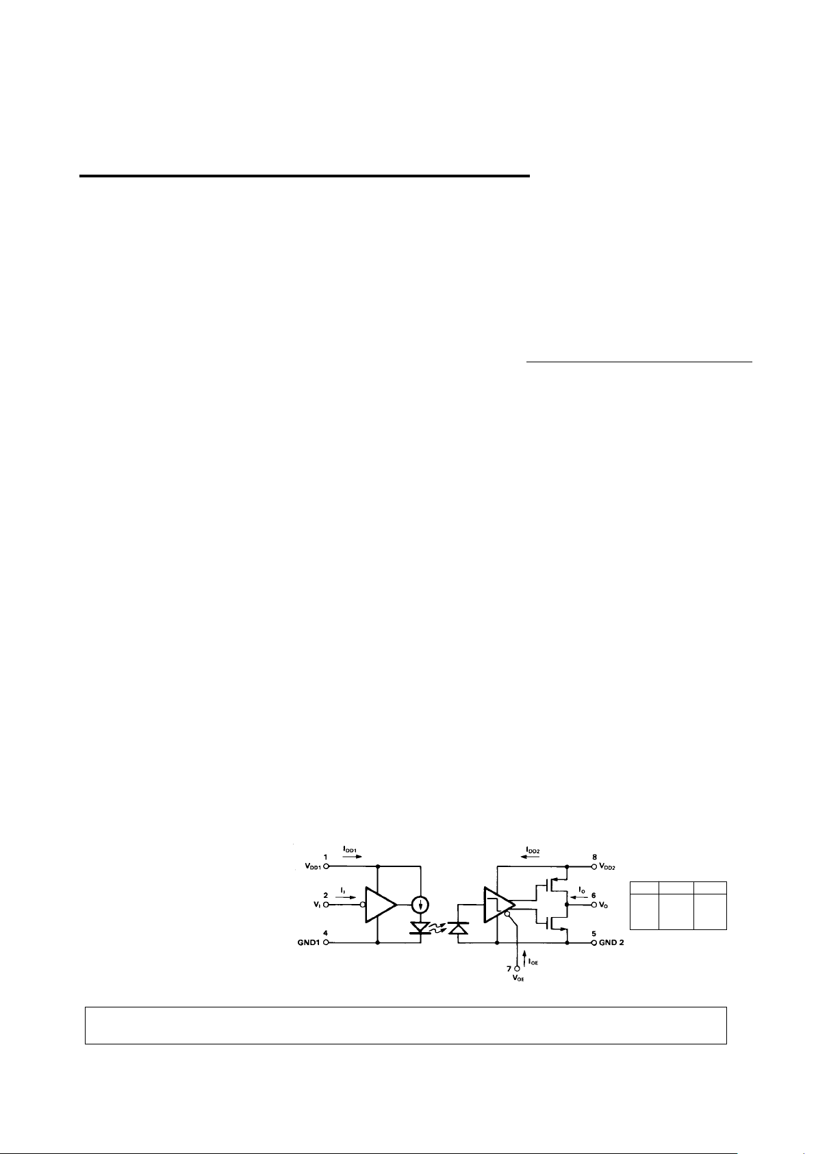
Description
The HCPL-7100/7101 optocoupler combines the latest CMOS IC
technology, a new high-speed
high-efficiency AlGaAs LED, and
an optimized light coupling system
to achieve outstanding performance with very low power
consumption. It requires only two
bypass capacitors for complete
CMOS/TTL compatibility.
Basic building blocks of the
HCPL-7100/7101 are a CMOS
LED driver IC, an AlGaAs LED,
and a CMOS detector IC. A CMOS
or TTL logic input signal controls
the LED driver IC which supplies
current to the LED. The detector
IC incorporates an integrated
photodiode, a high-speed transimpedance amplifier and a voltage
comparator with hysteresis. The
3-state output is CMOS and TTL
compatible and is controlled by
the output enable pin, VOE.
The HCPL-7100/7101 consumes
very little power, due to the
CMOS IC technology and the light
coupling system. The entire
optocoupler typically uses only 10
mA of supply current, including
the LED current.
World-wide safety approval and
3750 Vac/1 minute dielectric withstand is achieved with our
patented “light-pipe” optocoupler
packaging technology.
The HCPL-7100/7101 provides he
user with an easy-to-use CMOS or
TTL compatible optocoupler
ideally suited for a variety of
applications where high speed
and low power consumption are
desired.
HCPL-7100
HCPL-7101
Schematic
CAUTION: It is advised that normal static precautions be taken in handling and assembly of this component to
prevent damage and/or degradation which may be induced by ESD.
H
TRUTH TABLE
(POSITIVE LOGIC)
INPUT ENABLE OUTPUT
HH Z
LH Z
HL H
LL L
5965-3578E
Page 2
1-403
Ordering Information
HCPL-710x
0 = 15 MBd Minimum Data Rate
1 = 50 MBd Minimum Data Rate
Option yyy
300 = Gull Wing Surface Mount Lead Option
500 = Tape/Reel Package Option (1 k min.)
Option data sheets available. Contact your Hewlett-Packard sales representative or authorized distributor for
information.
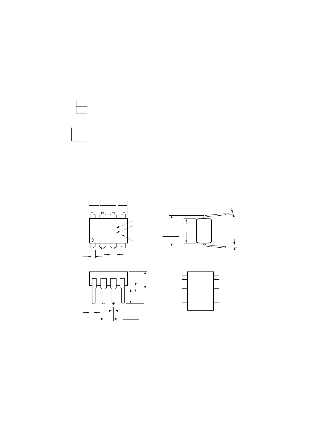
Package Outline Drawings
Standard DIP Package
9.40 (0.370)
9.90 (0.390)
1.78 (0.070) MAX.
1.19 (0.047) MAX.
HP XXXX
YYWW
DATE CODE
0.76 (0.030)
1.40 (0.055)
2.28 (0.090)
2.80 (0.110)
0.51 (0.020) MIN.
0.65 (0.025) MAX.
4.70 (0.185) MAX.
2.92 (0.115) MIN.
* PIN 3 IS THE ANODE OF THE INTERNAL LED AND
MUST BE LEFT UNCONNECTED FOR GUARANTEED
DATA SHEET PERFORMANCE.
DIMENSIONS IN MILLIMETERS AND (INCHES).
5678
4321
0.20 (0.008)
0.33 (0.013)
6.10 (0.240)
6.60 (0.260)
5° TYP.
7.36 (0.290)
7.88 (0.310)
1
2
3
4
8
7
6
5
GND1
V
DD1
V
I
*
GND2
V
DD2
V
OE
V
O
PIN ONE
TYPE NUMBER
UL
RECOGNITION
UR
* PIN 3 IS THE ANODE OF THE INTERNAL LED AND
MUST BE LEFT UNCONNECTED FOR GUARANTEED
DATA SHEET PERFORMANCE.
DIMENSIONS IN MILLIMETERS AND (INCHES).
Page 3
1-404
*Refer to Option 300 data sheet for more information.
0.635 ± 0.25
(0.025 ± 0.010)
12° NOM.
0.20 (0.008)
0.33 (0.013)
9.65 ± 0.25
(0.380 ± 0.010)
0.51 ± 0.130
(0.020 ± 0.005)
7.62 ± 0.25
(0.300 ± 0.010)
5
6
7
8
4
3
2
1
9.65 ± 0.25
(0.380 ± 0.010)
6.350 ± 0.25
(0.250 ± 0.010)
1.02 (0.040)
1.19 (0.047)
1.19 (0.047)
1.78 (0.070)
9.65 ± 0.25
(0.380 ± 0.010)
4.83
(0.190)
TYP.
0.380 (0.015)
0.635 (0.025)
PIN LOCATION (FOR REFERENCE ONLY)
1.080 ± 0.320
(0.043 ± 0.013)
4.19
(0.165)
MAX.
1.780
(0.070)
MAX.
1.19
(0.047)
MAX.
2.540
(0.100)
BSC
DIMENSIONS IN MILLIMETERS (INCHES).
TOLERANCES (UNLESS OTHERWISE SPECIFIED):
xx.xx = 0.01
xx.xxx = 0.005
HP XXXX
YYWW
DATE CODE
TYPE NUMBER
UL
RECOGNITION
UR
MOLDED
LEAD COPLANARITY
MAXIMUM: 0.102 (0.004)
Gull Wing Surface Mount Option 300*
Maximum Solder Reflow Thermal Profile
240
∆T = 115°C, 0.3°C/SEC
0
∆T = 100°C, 1.5°C/SEC
∆T = 145°C, 1°C/SEC
TIME – MINUTES
TEMPERATURE – °C
220
200
180
160
140
120
100
80
60
40
20
0
260
123456789101112
(NOTE: USE OF NON-CHLORINE ACTIVATED FLUXES IS RECOMMENDED.)
Page 4
1-405
VDE 0884 (06.92) Insulation Characteristics
Description Symbol Characteristic Unit
Installation classification per DIN VDE 0110, Table 1
for rated mains voltage ≤ 300 V rms I-IV
for rated mains voltage ≤ 600 V rms I-III
Climatic Classification 40/85/21
Pollution Degree (DIN VDE 0110, Table 1)* 2
Maximum Working Insulation Voltage V
IORM
848 V peak
Input to Output Test Voltage, Method b**
VPR = 1.875 x V
IORM
, Production test with tp = 1 sec, V
PR
1591 V peak
Partial discharge < 5 pC
Input to Output Test Voltage, Method a**
VPR = 1.5 x V
IORM
, Type and sample test, tp = 60 sec, V
PR
1273 V peak
Partial discharge < 5 pC
Highest Allowable Overvoltage** V
TR
6000 V peak
(Transient Overvoltage, tTR = 10 sec)
Safety-limiting values (Maximum values allowed in the event
of a failure, also see Figure 15)
Case Temperature T
S
175 °C
Input Power P
S,INPUT
80 mW
Output Power P
S,OUTPUT
250 mW
Insulation Resistance at TS, VIO = 500 V R
S
≥ 1 x 10
12
Ω
*This part may also be used in Pollution Degree 3 environments where the rated mains voltage is ≤ 300 V rms (per DIN VDE 0110).
**Refer to the front of the optocoupler section in the current catalog for a more detailed description of VDE 0884 and other product
safety requirements.
Insulation and Safety Related Specifications
Parameter Symbol Value Units Conditions
Min. External Air Gap L(IO1) 7.4 mm Measured from input terminals to output terminals,
(External Clearance) shortest distance through air
Min. External Tracking L(IO2) 8.0 mm Measured from input terminals to output terminals,
Path (External Creepage) shortest distance path along body
Min. Internal Plastic 0.5 mm Through insulation distance, conductor to conductor,
Gap (Internal Clearance) usually the direct distance between the photoemitter
and photodetector inside the optocoupler cavity
Tracking Resistance CTI 175 V DIN IEC 112/VDE 0303 PART 1
(Comparative
Tracking Index)
Isolation Group IIIa Material Group (DIN VDE 0110, 1/89, Table 1)
Option 300 – surface mount classification is Class A in accordance with CECC 00802.
Note: Optocouplers providing safe electrical separation per VDE 0884 do so only within the safety-limiting values to which they are
qualified. Protective cut-out switches must be used to ensure that the safety limits are not exceeded.
VDE
Approved according to VDE
0884/06.92
Regulatory Information
The HCPL-7100/1 has been
approved by the following
organizations:
UL
Recognized under UL 1577,
Component Recognition Program,
File E55361.
CSA
Approved under CSA Component
Acceptance Notice #5, File CA
88324.
Page 5
1-406
Parameter Symbol Min. Max. Unit
Storage Temperature T
S
-55 125 °C
Ambient Operating Temperature T
A
-40 85 °C
Supply Voltages V
DD1,2
0.0 5.5 V
Input Voltage V
I
-0.5 V
DD1
+ 0.5 V
Output Voltage V
O
-0.5 V
DD2
+ 0.5 V
Output Enable Voltage V
OE
-0.5 V
DD2
+ 0.5 V
Average Output Current I
O
25 mA
Package Power Dissipation P
PD
220 mW
Lead Solder Temperature T
LS
260 °C
(1.6 mm Below Seating Plane, 10 sec.)
Reflow Temperature Profile See Package Outline Drawings Section
Parameter Symbol Min. Max. Unit Test Conditions
Operating Temperature T
A
-40 85 °C
Supply Voltages V
DD1,2
4.5 5.5 V
Logic High Input Voltage V
IH
2.0 V
DD1
V
Logic Low Input Voltage V
IL
0.0 0.8 V
Logic High Output V
OEH
2.0 V
DD2
V Output in high impedance
Enable Voltage state
Logic Low Output V
OEL
0.0 0.8 V Output enabled
Enable Voltage
Input Signal Rise and tr, t
f
1ms
Fall Times
TTL Fanout N 6 Standard Loads
Absolute Maximum Ratings
Recommended Operating Conditions
Page 6

1-407
Electrical Specifications
Guaranteed across recommended operating conditions. Test conditions represent worst case values for the
parameter under test. Test conditions that are not specified can be anywhere within their operating range.
All typicals are at 25°C and 5 V supplies unless otherwise noted.
Parameter Symbol Min. Typ. Max. Unit Test Conditions Fig. Note
Logic Low Input Supply I
DD1L
5.2 10.0 mA V
DD1
= 5.5 V 1
Current V
I
= V
IL
Logic High Input Supply I
DD1H
0.3 0.6 mA VI = 4.5 V V
DD1
= 5.5 V 1
0.9 1.6 VI = 2.0 V
Logic Low Output I
DD2L
5.0 9.0 mA V
DD2
= 5.5 V
Supply Current V
OE
= V
OEL
VI = V
IL
Logic High Output I
DD2H
5.2 9.0 mA V
DD2
= 5.5 V
Supply Current V
OE
= V
OEL
IO = 0 mA
V
I
= V
IH
Tri-State Output Supply I
DD2Z
5.1 9.0 mA VOE = 4.5 V V
DD2
= 5.5 V
5.6 10.0 VOE = 2.0 V
Input Current I
I
-1 1 µAVI = V
DD1
or GND
V
DD1
= 5.5 V
Output Enable Current I
OE
-1 1 µAVOE = V
DD2
or GND
V
DD2
= 5.5 V
Logic High Output V
OH
4.4 5.0 IO = -20 µAV
DD2
= 4.5 V 6
Voltage V
I
= V
IH
VOE = V
OEL
Logic High Output I
OH
-7.5 -25 mA V
DD2
= 4.5 V 6
Current V
O
= 3.6 V
V
I
= V
IH
VOE = V
OEL
Logic Low Output V
OL
0.0 0.1 IO = 20 µAV
DD2
= 4.5 V 5
Voltage V
I
= V
IL
VOE = V
OEL
Logic Low Output I
OL
10.5 23 mA V
DD2
= 4.5 V 5
Current V
O
= 0.6 V
V
I
= V
IL
VOE = V
OEL
High Impedance I
OZ
-5 5 µAV
DD2
= 5.5 V
State Output V
OE
= V
OEH
Current VO = V
DD2
or GND
Input Capacitance C
I
4.3 pF f = 1 MHz 4
Input-Output R
I-O
10
12
10
13
Ω TA = 25°CV
I-O
= 500 V
dc
2
10
11
TA = 100°C
Input-Output C
I-O
0.7 pF f = 1 MHz 2
Capacitance
*The Input-Output Momentary Withstand Voltage is a dielectric voltage rating that should not be interpreted as an input-output
continuous voltage rating. For the continuous voltage rating refer to the VDE 0884 Insulation Characteristics Table (if applicable),
your equipment level safety specification, or HP Application Note 1074, “Optocoupler Input-Output Endurance Voltage.”
Current
3.7 4.7 IO = -6.0 mA
0.15 0.4 I
O
= 6.0 mA
Resistance
Current
4.0 4.8 V IO = -4.0 mA
0.1 0.3 V IO = 4.0 mA
Page 7

1-408
Parameter Symbol Device Min. Typ. Max. Unit Test Conditions Fig. Note
Propagation t
PHL
HCPL-7100 70 ns CL = 50 pF 7, 8 5, 6
Delay Time CMOS Signal Levels
to Logic HCPL-7101 28 40
Low Output
HCPL-7100 70 ns C
L
= 15 pF
TTL Signal Levels
HCPL-7101 40
Propagation t
PLH
HCPL-7100 70 ns CL = 50 pF 7, 8 5, 6
Delay Time CMOS Signal Levels
to Logic HCPL-7101 27 40
High Output
HCPL-7100 70 ns C
L
= 15 pF
TTL Signal Levels
HCPL-7101 40
Pulse Width PWD HCPL-7100 20 ns C
L
= 50 pF 7, 9 6, 7
Distortion CMOS Signal Levels
|t
PHL-tPLH
| HCPL-7101 2 6
HCPL-7100 20 ns C
L
= 15 pF
TTL Signal Levels
HCPL-7101 6
Data Rate HCPL-7100 15 MBd % PWD < 30% 8
HCPL-7101 50 65
Propagation t
PSK
HCPL-7101 10 ns 10 9
Delay Skew
Output Rise t
R
HCPL-7100 12 ns CL = 50 pF 7
Time CMOS Signal Levels
(10-90%) HCPL-7101 10
Output Fall t
F
HCPL-7100 8 ns CL = 50 pF 7
Time CMOS Signal Levels
(90-10%) HCPL-7101 7
Random Jitter RJ HCPL-7101 50 ps rms V
1
= 0-5 V square wave,
f = 25 MHz, input rise/
fall time = 5 ns.
R
L
= 10 kΩ,
C
L
= 5 pF.
TTL Threshold Levels.
Propagation t
PZH
13 ns CL = 50 pF 12 6
Delay Time From CMOS Signal Levels
Output Enabled
to Logic High 12 ns C
L
= 15 pF
Output TTL Signal Levels
Propagation t
PZL
11 ns CL = 50 pF 12 6
Delay Time From CMOS Signal Levels
Output Enabled
to Logic Low 10 ns C
L
= 15 pF
Output TTL Signal Levels
Switching Specifications
Guaranteed across recommended operating conditions. Test conditions represent worst case values for the
parameter under test. Test conditions that are not specified can be anywhere within their operating range. All
typicals are at 25°C and 5 V supplies unless otherwise noted.
Page 8

1-409
Package Characteristics
Guaranteed across recommended operating conditions. Test conditions represent worst case value for the
parameter under test. Test conditions that are not specified can be anywhere within their operating range.
All typicals are at TA = 25°C and 5 V supplies unless otherwise noted.
Parameter Sym. Min. Typ. Max. Units Test Conditions Fig. Note
Input-Output V
ISO
3750 V rms t = 1 min., RH < 50%, 2, 3
Momentary TA = 25°C
Withstand Voltage*
Input-Output R
I-O
10
12
10
13
Ω TA = 25°CV
I-O
= 500 Vdc 2
Resistance 10
11
TA =100° C
Input-Output C
I-O
0.7 pF f = 1 MHz 2
Capacitance
*The Input-Output Momentary Withstand Voltage is a dielectric voltage rating that should not be interpreted as an input-output
continuous voltage rating. For the continuous voltage rating refer to the VDE 0884 Insulation Characteristics Table (if applicable),
your equipment level safety specification or HP Application Note 1074 entitled “Optocoupler Input-Output Endurance Voltage.”
Switching Specifications (cont.)
Guaranteed across recommended operating conditions. Test conditions represent worst case values for the
parameter under test. Test conditions that are not specified can be anywhere within their operating range. All
typicals are at 25°C and 5 V supplies unless otherwise noted.
Parameter Symbol Device Min. Typ. Max. Unit Test Conditions Fig. Note
Propagation t
PHZ
12 ns CL = 50 pF 12 6
Delay Time from CMOS Signal Levels
Logic High to
Output Disabled 12 ns C
L
= 15 pF
TTL Signal Levels
Propagation t
PLZ
9nsC
L
= 50 pF 12 6
Delay Time from CMOS Signal Levels
Logic Low to
Output Disabled 11 ns C
L
= 15 pF
TTL Signal Levels
Common Mode |CMH| HCPL-7100 1000 V/µsVCM = 50 V VI = V
IH
13, 10
V
D
> 3.2 V 14
HCPL-7101 2000 V
CM
= 200 V
Common Mode |CM
L
| HCPL-7100 1000 V/µsVCM = 50 V VI = V
IL
13, 10
VD < 0.8 V 14
HCPL-7101 2000 V
CM
= 200 V
Input Dynamic C
PD1
68 pF 11
Power Dissipation
Capacitance
Output Dynamic C
PD2
10 pF 11
Power Dissipation
Capacitance
Transient
Immunity at
Logic High
Output
Transient
Immunity at
Logic Low
Output
Page 9

1-410
Notes:
1. The LED is OFF when the VI is high and ON when VI is low.
2. Device considered a two terminal device; pins 1-4 shorted together and pins 5-8 shorted together.
3. In accordance with UL 1577, for devices with minimum V
ISO
specified at 3750 V rms, each optocoupler is proof-tested by applying an
insulation test voltage greater than 4500 V rms for one second (leakage current detection limit I
I-O
< 5 µA). This test is performed
before the method b, 100% production test for partial discharge shown in the VDE 0884 Insulation Characteristics Table.
4. CI is the capacitance measured at pin 2 (VI).
5. t
PHL
propagation delay is measured from the 50% level on the falling edge of the VI signal to the logic switching level of the VO signal.
t
PLH
propagation delay is measured from the 50% level on the rising edge of the VI signal to the logic switching level of the VO signal.
6. The logic switching levels are 1.5 V for TTL signals (0-3 V) and 2.5 V for CMOS signals (0-5 V).
7. PWD is defined as |t
PHL
- t
PLH
|. %PWD (percent pulse width distortion) is equal to PWD in ns divided by symbol duration (bit length)
in ns.
8. Minimum data rate is calculated as follows: %PWD/PWD where %PWD is typically chosen by the design engineer (30% is common).
9. t
PSK
is equal to the worst case difference in t
PHL
and/or t
PLH
that will be seen between units at the same temperature, supply voltage,
and output load within the recommended operating condition range.
10. CMH is the maximum common mode voltage slew rate that can be sustained while maintaining VO > 3.2 V. CML is the maximum
common mode voltage slew rate that can be sustained while maintaining VO < 0.8 V. The common mode voltage slew rates apply to
both rising and falling common mode voltage edges.
11. Unloaded dynamic power dissipation is calculated as follows: CPD • V
DD
2 •
f + IDD • VDD where f is switching frequency in MHz.
Figure 1. Recommended Application Circuit.
Figure 2. Recommended Printed Circuit Board Layout.
Page 10

1-411
Figure 5. Typical Logic Low Output Voltage vs. Logic Low
Output Current.
Figure 6. Typical Logic High Output Voltage vs. Logic High
Output Current.
V
DD2
= 5.0 V
V
DD2
= 5.0 V
Figure 4. Typical Input Voltage Switching Threshold vs.
Input Supply Voltage.
Figure 3. Typical Output Voltage vs. Input Voltage.
V
O
(V)
0
0
VI (V)
5.00
4.00
5.50
1.00
4.001.00 2.00 3.00
2.50
5.00
4.50
3.50
3.00
2.00
1.50
0.50
V
DD1
= 5.0 V
85 °C
-40 °C
25 °C
Page 11

1-412
Figure 8. HCPL-7101 Typical Propagation Delay vs.
Temperature.
Figure 9. HCPL-7101 Typical Pulse Width Distortion vs.
Temperature.
Figure 7. Test Circuit for Propagation Delay, Rise Time and Fall Time.
V
DD1
= 5.0 V
V
DD2
= 5.0 V
V
DD1
= 5.0 V
V
DD2
= 5.0 V
Page 12

1-413
Figure 11. Parallel Data Transmission Example.Figure 10. Propagation Delay Skew Waveform.
Figure 12. Test Circuit for 3-State Output Enable and Disable Propagation Delays.
Page 13

1-414
Figure 15. Dependence of Safety-Limiting Data on
Ambient Temperature.
Figure 13. Test Circuit for Common Mode Transient
Immunity and Typical Waveforms.
Figure 14. Typical Common Mode
Transient Immunity vs. Common Mode
Transient Voltage.
V
DD1
= 5.0 V
V
DD2
= 5.0 V
T
A
= 25 °C
OUTPUT, V
O
V
OL
P
S
– POWER – mW
0
0
TA – TEMPERATURE – °C
180
400
12040 80 160
100
200
300
OUTPUT POWER, P
S
INPUT POWER, P
S
20 60 100 140
175
Page 14

1-415
HCPL-7100/7101
Application Information
The HCPL-7100/7101 is
extremely easy to use. Because
the optocoupler uses high-speed
CMOS IC technology, the inputs
and output are fully compatible
with all +5 V TTL and CMOS
logic. TTL or CMOS logic can be
connected directly to the inputs
and output; no external interface
circuitry is required.
As shown in Figure 1, the only
external components required for
proper operation are two ceramic
bypass capacitors. Capacitor
values should be between 0.01 µF
and 0.1 µF. For each capacitor,
the total lead length between both
ends of the capacitor and the
power-supply pins should not
exceed 20 mm. Figure 2
illustrates the recommended
printed circuit board layout for
the HCPL-7100/7101.
Propagation Delay, PulseWidth Distortion, and
Propagation Delay Skew
Propagation delay is a figure of
merit which describes how
quickly a logic signal propagates
through a system. The propagation delay from low to high (t
PLH
)
is the amount of time required for
an input signal to propagate to
the output, causing the output to
change from low to high.
Similarly, the propagation delay
from high to low (t
PHL
) is the
amount of time required for the
input signal to propagate to the
output, causing the output to
change from high to low (see
Figure 7).
Pulse-width distortion (PWD)
results when t
PLH
and t
PHL
differ in
value. PWD is defined as the
difference between t
PLH
and t
PHL
and often determines the maximum data rate capability of a
transmission system. PWD can be
expressed in percent by dividing
the PWD (in ns) by the minimum
pulse width (in ns) being
transmitted. Typically, PWD on
the order of 20-30% of the
minimum pulse width is tolerable;
the exact figure depends on the
particular application (RS232,
RS422, T-1, etc.).
Propagation delay skew, t
PSK
, is
an important parameter to consider in parallel data applications
where synchronization of signals
on parallel data lines is a concern.
If the parallel data is being sent
through a group of optocouplers,
differences in propagation delays
will cause the data to arrive at the
outputs of the optocouplers at
different times. If this difference
in propagation delays is large
enough, it will determine the
maximum rate at which parallel
data can be sent through the
optocouplers.
Propagation delay skew is defined
as the difference between the
minimum and maximum propagation delays, either t
PLH
or t
PHL
, for
any given group of optocouplers
which are operating under the
same conditions (i.e., the same
supply voltage, output load, and
operating temperature). As illustrated in Figure 10, if the inputs
of a group of optocouplers are
switched either ON or OFF at the
same time, t
PSK
is the difference
between the shortest propagation
delay, either t
PLH
or t
PHL
, and the
longest propagation delay, either
t
PLH
or t
PHL
.
As mentioned earlier, t
PSK
can
determine the maximum parallel
data transmission rate. Figure 11
is the timing diagram of a typical
parallel data application with both
the clock and the data lines being
sent through optocouplers. The
figure shows data and clock
signals at the inputs and outputs
of the optocouplers. To obtain the
maximum data transmission rate,
both edges of the clock signal are
being used to clock the data; if
only one edge were used, the
clock signal would need to be
twice as fast.
Propagation delay skew represents the uncertainty of where an
edge might be after being sent
through an optocoupler. Figure
11 shows that there will be
uncertainty in both the data and
the clock lines. It is important
that these two areas of uncertainty
not overlap, otherwise the clock
signal might arrive before all of
the data outputs have settled, or
some of the data outputs may
start to change before the clock
signal has arrived. From these
considerations, the absolute
minimum pulse width that can be
sent through optocouplers in a
parallel application is twice t
PSK
. A
cautious design should use a
slightly longer pulse width to
ensure that any additional
uncertainty in the rest of the
circuit does not cause a problem.
The HCPL-7101 optocoupler offers
the advantages of guaranteed
specifications for propagation
delays, pulse-width distortion and
propagation delay skew over the
recommended temperature, and
power supply ranges.
 Loading...