

Page 1
tm
HCPL062N 3.3V Dual Channel High Speed-10 MBit/s Logic Gate Optocouplers
July 2006
HCPL062N
3.3V Dual Channel High Speed-10 MBit/s Logic Gate
Optocouplers
Features
■
Compact SO8 package
Very high speed – 10MBit/s
■
■
Superior CMR – 25kV/µs minimum (1,000 volts
common mode)
Logic gate output
■
■
Wired OR-open collector
Fixed threshold detector design minimizes thermal
■
impact on switching times
■
U.L. recognized (File # E90700)
Applications
Ground loop elimination
■
■
Field buses
Line receiver, data transmission
■
■
Data multiplexing
■
Switching power supplies
Pulse transformer replacement
■
■
Computer-peripheral interface
Instrumentation input/output isolation
■
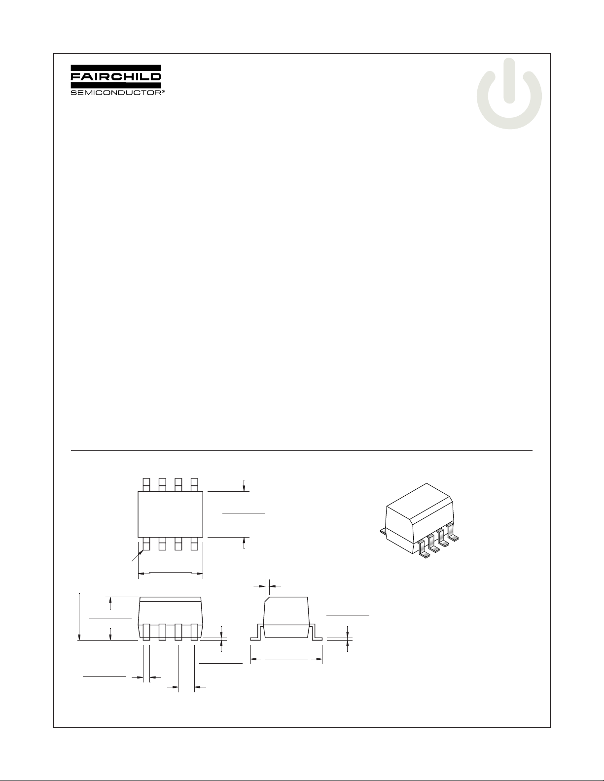
Package Dimensions
Description
The HCPL062N optocouplers consist of an AlGaAs LED,
optically coupled to a very high speed integrated photodetector logic gate consisting of bipolar transistors on a
CMOS process for reduced power consumption. The
output features an open collector, thereby permitting
wired OR outputs. The devices are housed in a compact
small-outline package. The coupled parameters are
guaranteed over the temperature range of -40°C to
+85°C. An internal noise shield and provides superior
common mode rejection.
NG PLANE
SEATI
Pin 1
0.143 (3.63)
0.123 (3.13)
0.021 (0.53)
0.011 (0.28)
0.202 (5.13)
0.182 (4.63)
Note:
All dimensions are in inches (millimeters)
©2006 Fairchild Semiconductor Corporation
HCPL062N Rev. 1.0.0
0.164 (4.16)
0.144 (3.66)
0.008 (0.20)
0.003 (0.08)
0.050 (1.27)
TYP
0.019 (0.48)
0.244 (6.19)
0.224 (5.69)
1
0.010 (0.25)
0.006 (0.16)
Lead Coplanarity : 0.004 (0.10) MAX
www.fairchildsemi.com
Page 2
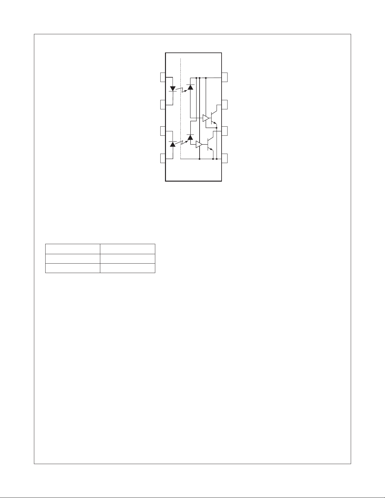
Circuit Drawing
HCPL062N 3.3V Dual Channel High Speed-10 MBit/s Logic Gate Optocouplers
(1)
+
1
V
F1
_
2
_
3
V
F2
+
4 5
8
7
6
V
CC
V
01
V
02
GND
Note:
1. The V
or solid tantalum capacitor with good high frequency characteristic and should be connected no further than 3mm
from the V
supply to each optoisolator must be bypassed by a 0.1µF capacitor or larger. This can be either a ceramic
CC
and GND pins of each device.
CC
Truth Table (Positive Logic)
Input Output
HL
LH
A 0.1µF bypass capacitor must be connected between pins 8 and 5.
HCPL062N Rev. 1.0.0
2
www.fairchildsemi.com
Page 3
HCPL062N 3.3V Dual Channel High Speed-10 MBit/s Logic Gate Optocouplers
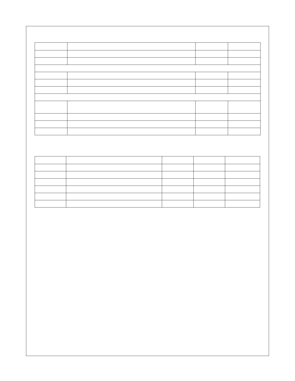
Absolute Maximum Ratings
(No derating required up to 85°C)
Symbol Parameter Value Units
T
STG
T
OPR
EMITTER
I
F
V
R
P
I
DETECTOR
V
CC
(1 minute max)
I
O
V
O
P
O
Storage Temperature -40 to +125 °C
Operating Temperature -40 to +85 °C
DC/Average Forward Input Current (each channel) 50 mA
Reverse Input Voltage (each channel) 5.0 V
Power Dissipation 45 mW
Supply Voltage 7.0 V
Output Current (each channel) 15 mA
Output Voltage (each channel) 7.0 V
Collector Output Power Dissipation 85 mW
Recommended Operating Conditions
Symbol Parameter Min. Max. Units
I
FL
I
FH
V
CC
T
A
NFan Out (TTL load) – 5 TTL Loads
R
L
Note:
2. 6.3mA is a guard banded value which allows for at least 20% CTR degradation. Initial input current threshold value
is 5.0mA or less
Input Current, Low Level 0 250 µA
Input Current, High Level 6.3
(2)
15 mA
Supply Voltage, Output 2.7 3.3 V
Operating Temperature -40 +85 °C
Output Pull-up 330 4K
Ω
HCPL062N Rev. 1.0.0
3
www.fairchildsemi.com
Page 4

∆
/ ∆
HCPL062N 3.3V Dual Channel High Speed-10 MBit/s Logic Gate Optocouplers
Electrical Characteristics
(T
= -40°C to +85°C Unless otherwise specified.)
A
Individual Component Characteristics
Symbol Parameter Test Conditions Min. Typ.
EMITTER
V
B
Input Forward Voltage I
F
Input Reverse Breakdown
VR
= 10mA – – 1.8 V
F
T
=25°C – – 1.75
A
I
= 10µA 5.0 – – V
R
Voltage
V
T
F
Input Diode Temperature
A
I
= 10mA – -1.5 – mV/°C
F
Coefficient
DETECTOR
I
CCH
I
CCL
Switching Characteristics
High Level Supply Current I
Low Level Supply Current I
(T
= -40°C to +85°C, V
A
= 0mA, V
F
= 10mA, V
F
CC
= 3.3V – 7.1 10 mA
CC
= 3.3V – 6.7 15 mA
CC
= 3.3V, I
= 7.5 mA Unless otherwise specified.)
F
Symbol AC Characteristics Test Conditions Min. Typ.
T
PLH
Propagation Delay
Time to Output High
Level
T
PHL
Propagation Delay
Time to Output Low
Level
|T
–T
PHL
| Pulse Width Distortion R
PLH
t
Output Rise Time
r
(10–90%)
t
Output Fall Time
f
(90–10%)
| Common Mode
|CM
H
Tr ansient Immunity
(at Output High Level)
| Common Mode
|CM
L
Tr ansient Immunity
(at Output Low Level)
R
= 350 Ω , C
L
= 15pF
L
Note 4, Fig. 10
= 350 Ω , C
R
L
= 15pF
L
Note 5, Fig. 10
= 350 Ω , C
L
= 15pF
L
Fig. 10
R
= 350 Ω , C
L
= 15pF)
L
Note 6, Fig. 10
R
= 350 Ω , C
L
= 15pF
L
Note 7, Fig. 10
R
= 350 Ω , T
L
= 3.3V, V
V
CC
|V
| = 1,000V
CM
= 25°C, I
A
O(Min.)
Notes 8, 11, Fig. 11
R
= 350 Ω , T
L
= 3.3V, V
V
CC
|V
| = 1,000V
CM
=25°C, I
A
O(Max.)
Notes 9, 11, Fig. 11
F
= 2V
= 7.5mA,
F
= 0.8V
= 0 mA,
––90ns
––75ns
––25ns
–16–ns
–4–ns
25,000 – – V/µs
25,000 – – V/µs
(3)
Max. Unit
(3)
Max. Unit
HCPL062N Rev. 1.0.0
4
www.fairchildsemi.com
Page 5
HCPL062N 3.3V Dual Channel High Speed-10 MBit/s Logic Gate Optocouplers
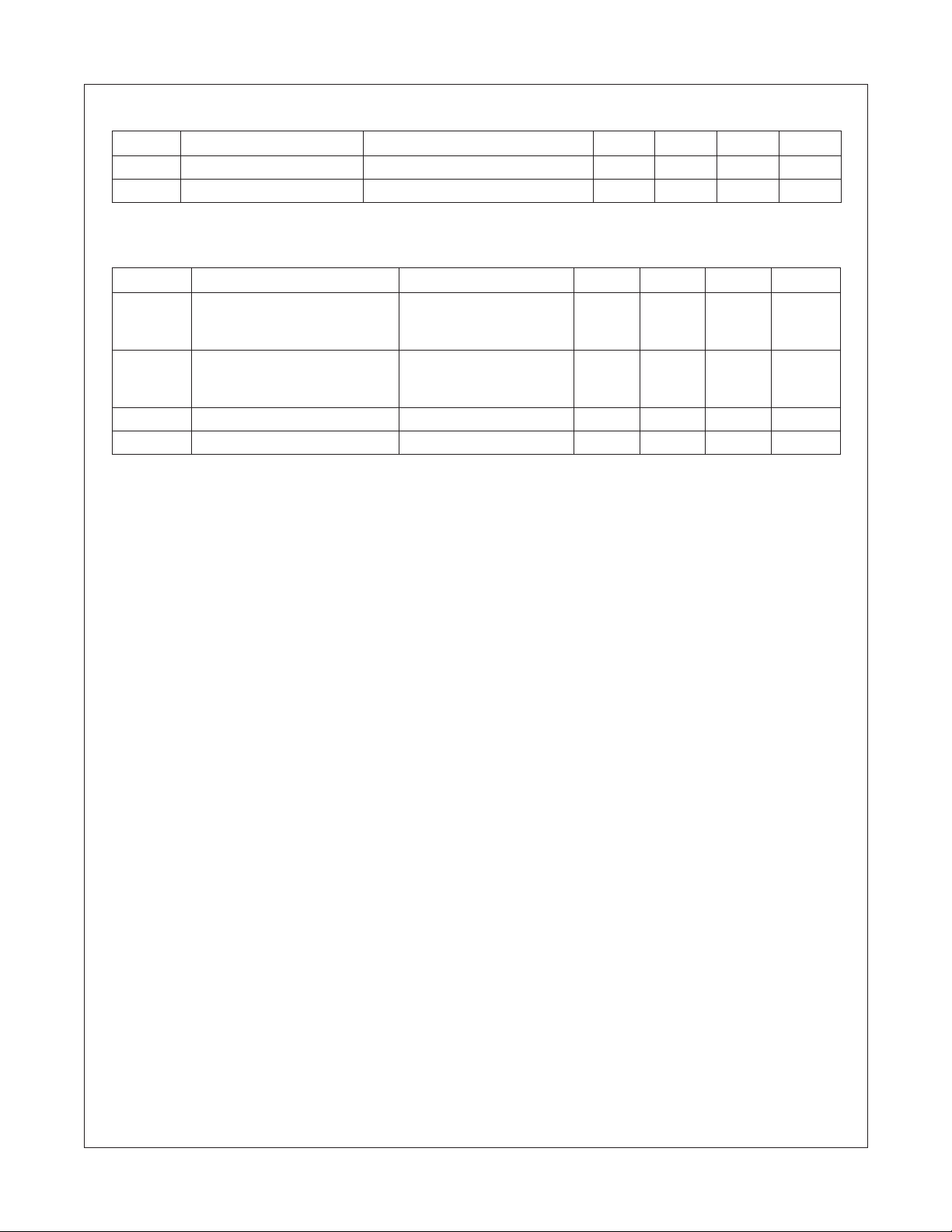
Transfer Characteristics
Symbol DC Characteristics Test Conditions Min. Typ.
V
I
Low Level Output Voltage VCC = 3.3V, IF = 5mA, IOL = 13mA – – 0.6 V
OL
Input Threshold Current VCC = 3.3V, VO = 0.6V, IOL = 13mA – – 5 mA
FT
Isolation Characteristics
Symbol Characteristics Test Conditions Min. Typ.
I
I-O
V
ISO
Input-Output
Insulation Leakage Current
Withstand Insulation Test
Voltage
(T
= -40°C to +85°C Unless otherwise specified.)
A
(T
= -40°C to +85°C Unless otherwise specified.)
A
Relative humidity = 45%
T
= 25°C, t = 5 sec.
A
V
= 3000 VDC, Note 10
I-O
RH < 50%, TA = 25°C
I
≤ 2µA, t = 1 min.,
I-O
(3)
Max. Unit
(3)
Max. Unit
––1.0 µA
2500 – – V
RMS
Note 10
R
I-O
C
I-O
Resistance (Input to Output) V
= 500V, Note 10 – 10
I-O
Capacitance (Input to Output) f = 1MHz, Note 10 – 0.6 – pF
12
– Ω
Notes:
3. All typical values are at V
4. t
5. t
6. t
7. t
8. CM
9. CM
– Propagation delay is measured from the 3.75 mA level on the HIGH to LOW transition of the input current
PLH
pulse to the 1.5V level on the LOW to HIGH transition of the output voltage pulse.
– Propagation delay is measured from the 3.75 mA level on the LOW to HIGH transition of the input current
PHL
pulse to the 1.5V level on the HIGH to LOW transition of the output voltage pulse.
– Rise time is measured from the 90% to the 10% levels on the LOW to HIGH transition of the output pulse.
r
– Fall time is measured from the 10% to the 90% levels on the HIGH to LOW transition of the output pulse.
f
– The maximum tolerable rate of rise of the common mode voltage to ensure the output will remain in the high
H
state (i.e., V
– The maximum tolerable rate of fall of the common mode voltage to ensure the output will remain in the low
L
output state (i.e., V
> 2.0 V). Measured in volts per microsecond (V/µs).
OUT
OUT
= 3.3V, T
CC
= 25°C unless otherwise specified.
A
< 0.8 V). Measured in volts per microsecond (V/µs).
10. Device considered a two-terminal device: Pins 1,2,3 and 4 shorted together, and Pins 5,6,7 and 8 shorted together.
11. The power supply bypass capacitors must be no further than 3mm from the leads of the optocoupler. A low
inductance ground plane width of with ≤ 5nHy of series lead inductance is required.
HCPL062N Rev. 1.0.0
5
www.fairchildsemi.com
Page 6
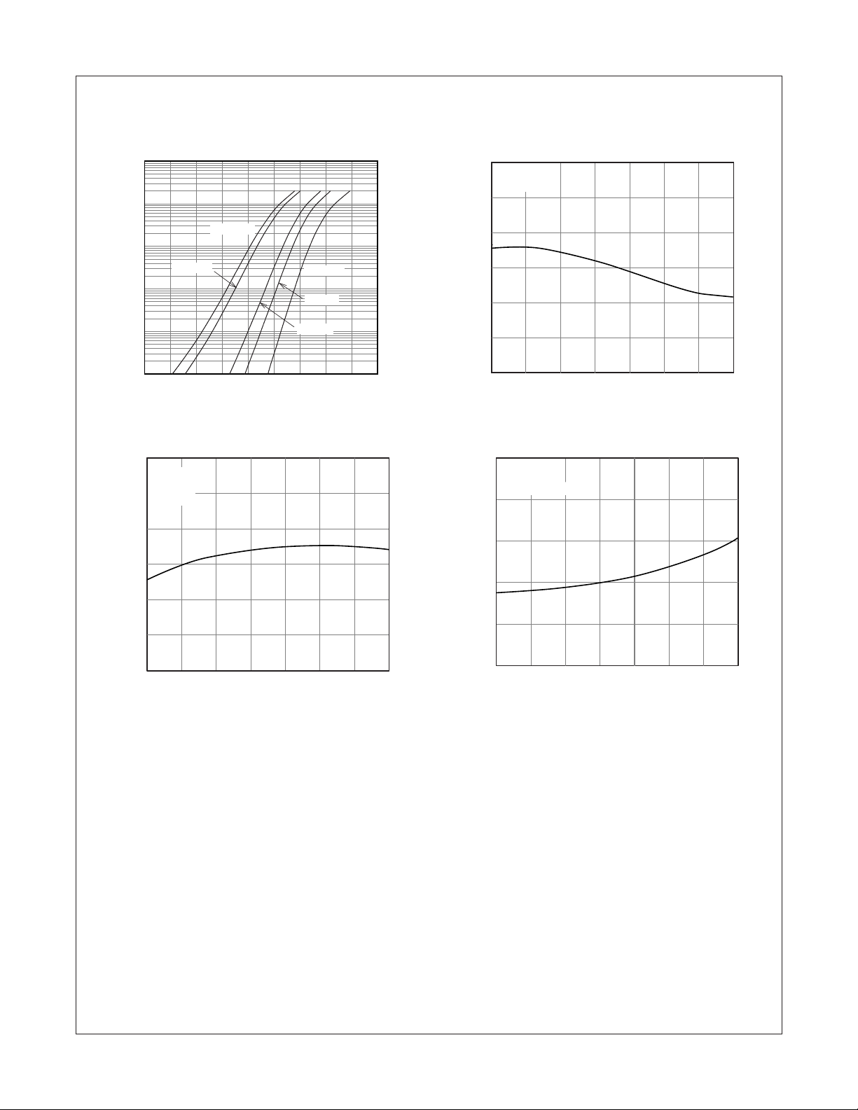
Typical Performance Curves
HCPL062N 3.3V Dual Channel High Speed-10 MBit/s Logic Gate Optocouplers
Fig. 1 Forward Current vs. Forward Voltage
100
10
TA = 100oC
1
TA = 85oC
0.1
– FORWARD CURRENT (mA)
F
0.01
I
0.001
0.8 0.9 1.0 1.1 1.2 1.3 1.4 1.5 1.6 1.7
TA = -40oC
TA = 0oC
TA = 25oC
VF – FORWARD VOLTAGE (V)
Fig. 3 Low Level Output Current vs. Ambient Temperature
40
VCC = 3.3V
= 0.6V
V
OL
35
= 5mA
I
F
30
25
20
Fig. 2 High Level Output Current vs.
Ambient Temperature
12
VO = VCC = 3.3V
I
= 250µA
F
10
8
6
4
2
– HIGH LEVEL OUTPUT CURRENT (nA)
OH
I
0
-40 -20 0 20 40 60 80 100
TA – AMBIENT TEMPERATURE (°C)
Fig. 4 Input Threshold Current vs. Temperature
2.5
VCC = 3.3V
= 0.6V
V
O
= 350Ω, 1kΩ, 4kΩ
R
L
2.0
1.5
1.0
15
- LOW LEVEL OUTPUT CURRENT (mA)
OL
I
10
-40 -20 0 20 406080100
TA – AMBIENT TEMPERATURE (°C)
0.5
- INPUT THRESHOLD CURRENT (mA)
TH
I
0.0
-40 -20 0 20 406080100
T
– AMBIENT TEMPERATURE (°C)
A
HCPL062N Rev. 1.0.0
6 www.fairchildsemi.com
Page 7
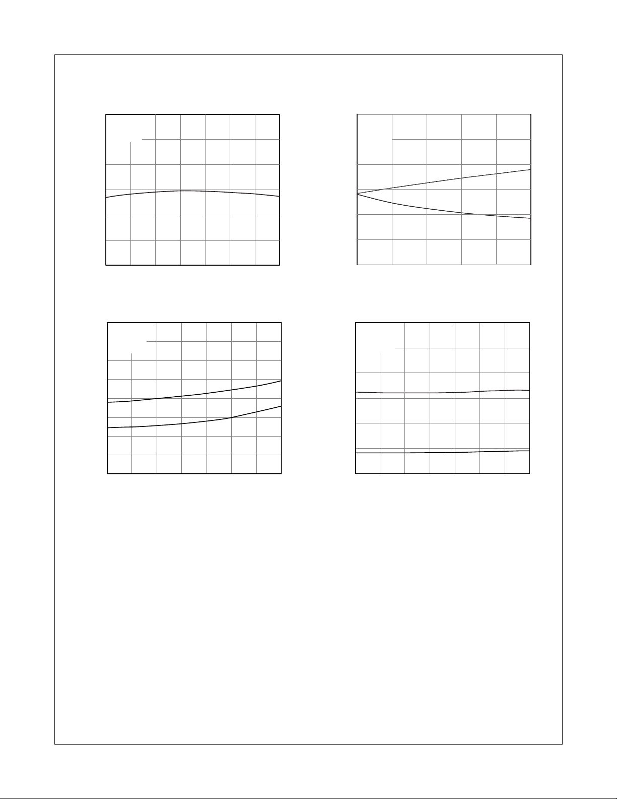
Typical Performance Curves (Continued)
HCPL062N 3.3V Dual Channel High Speed-10 MBit/s Logic Gate Optocouplers
Fig. 5 Pulse Width Distortion vs. Ambient Temperature
30
= 3.3V
V
CC
= 7.5mA
I
F
R
= 350Ω
L
25
20
15
10
5
PWD – PULSE WIDTH DISTORTION (ns)
0
-40 -20 0 20 406080100
TA – AMBIENT TEMPERATURE (˚C)
Fig. 6 Propagation Delay vs. Pulse Input Current
120
= 3.3V
V
CC
RL = 350Ω
= 25oC
T
A
100
80
60
40
– PROPAGATION DELAY (ns)
P
t
20
0
5791113 15
IF – PULSE INPUT CURRENT (mA)
t
PLH
t
PHL
Fig. 7 Propagation Delay vs. Ambient Temperature Fig. 8 Rise and Fall Times vs. Ambient Temperature
100
V
= 3.3V
CC
= 7.5mA
I
F
90
R
= 350Ω
L
80
70
60
t
PLH
30
= 3.3V
V
CC
= 7.5mA
I
F
R
= 350Ω
25
L
20
t
15
r
50
40
– PROPAGATION DELAY (ns)
P
t
30
20
-40 -20 0 20 406080100
– AMBIENT TEMPERATURE (˚C)
T
A
t
PHL
10
– RISE, FALL TIMES (ns)
f
, t
r
t
5
0
-40 -20 0 20 406080100
t
f
TA – AMBIENT TEMPERATURE (˚C)
HCPL062N Rev. 1.0.0
7 www.fairchildsemi.com
Page 8
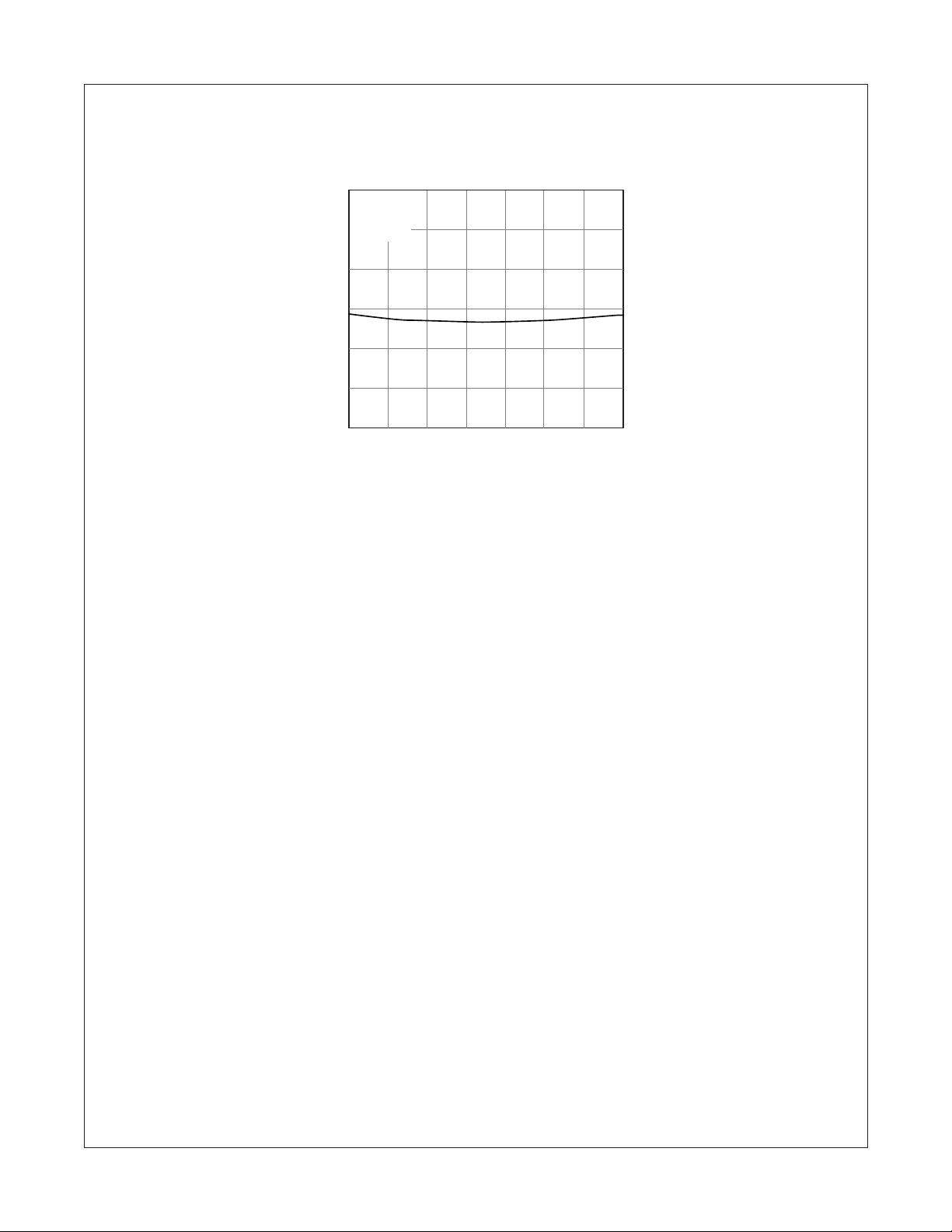
Typical Performance Curves (Continued)
Fig. 9 Low Level Output Voltage vs. Ambient Temperature
0.6
VCC = 3.3V
= 13mA
I
O
0.5
I
= 5mA
F
0.4
0.3
0.2
0.1
– LOW LEVEL OUTPUT VOLTAGE (V)
OL
V
0.0
0-20 0 20 406080100
-4
TA – AMBIENT TEMPERATURE (˚C)
HCPL062N 3.3V Dual Channel High Speed-10 MBit/s Logic Gate Optocouplers
HCPL062N Rev. 1.0.0
8 www.fairchildsemi.com
Page 9
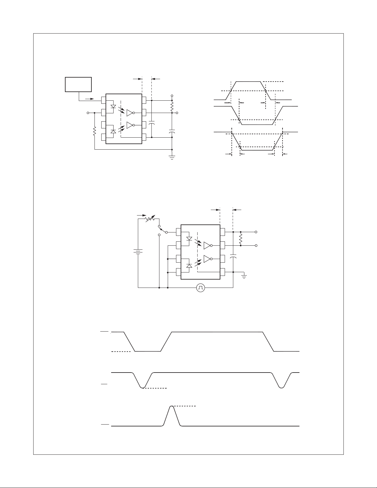
Test Circuits
HCPL062N 3.3V Dual Channel High Speed-10 MBit/s Logic Gate Optocouplers
Pulse Gen.
= 50 Ω
Z
O
tf = tr = 5 ns
Input
Monitoring
Node
Fig. 10 Test Circuit and Waveforms for t
≤3mm spacing
I
F
R
M
Dual Channel
1
2
3
4
V
CC
GND
8
7
6
5
0.1µF
Bypass
+3.3V
R
L
Output V
Monitoring
Node
*
C
L
Input
(I )
F
O
Output
(V )
O
Output
(V )
O
t
PHL
PLH
, t
t
f
PHL, tr
90%
10%
and t
t
PLH
f
1.5 V
t
r
Fig. 11 Test Circuit and Waveforms for Common Mode Transient Immunity
I
F
Dual Channel
B
A
1
2
V
FF
3
4
V
CC
GND
8
7
6
5
≤3mm spacing
R
L
0.1µF
Bypass
+3.3V
Output V
O
Monitoring
Node
I = 7.5 mA
F
I = 3.75 mA
F
V
0V
Peak
3.3V
V
V
0.5 V
CM
V
CM
+–
Pulse
Generator
Z
= 50 Ω
O
CM
CM
H
L
O
O
V (Min)
O
Switching Pos. (A), I = 0
F
V (Max)
O
Switching Pos. (B), I = 7.5 mA
F
HCPL062N Rev. 1.0.0
9 www.fairchildsemi.com
Page 10
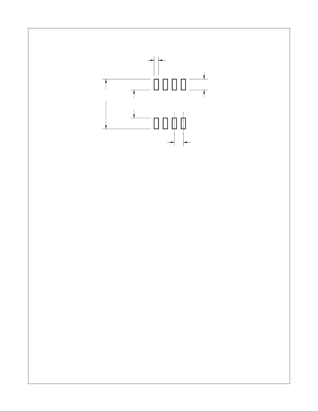
Footprint
8-Pin Small Outline
HCPL062N 3.3V Dual Channel High Speed-10 MBit/s Logic Gate Optocouplers
0.024 (0.61)
0.060 (1.52)
0.275 (6.99)
0.155 (3.94)
0.050 (1.27)
HCPL062N Rev. 1.0.0
10 www.fairchildsemi.com
Page 11
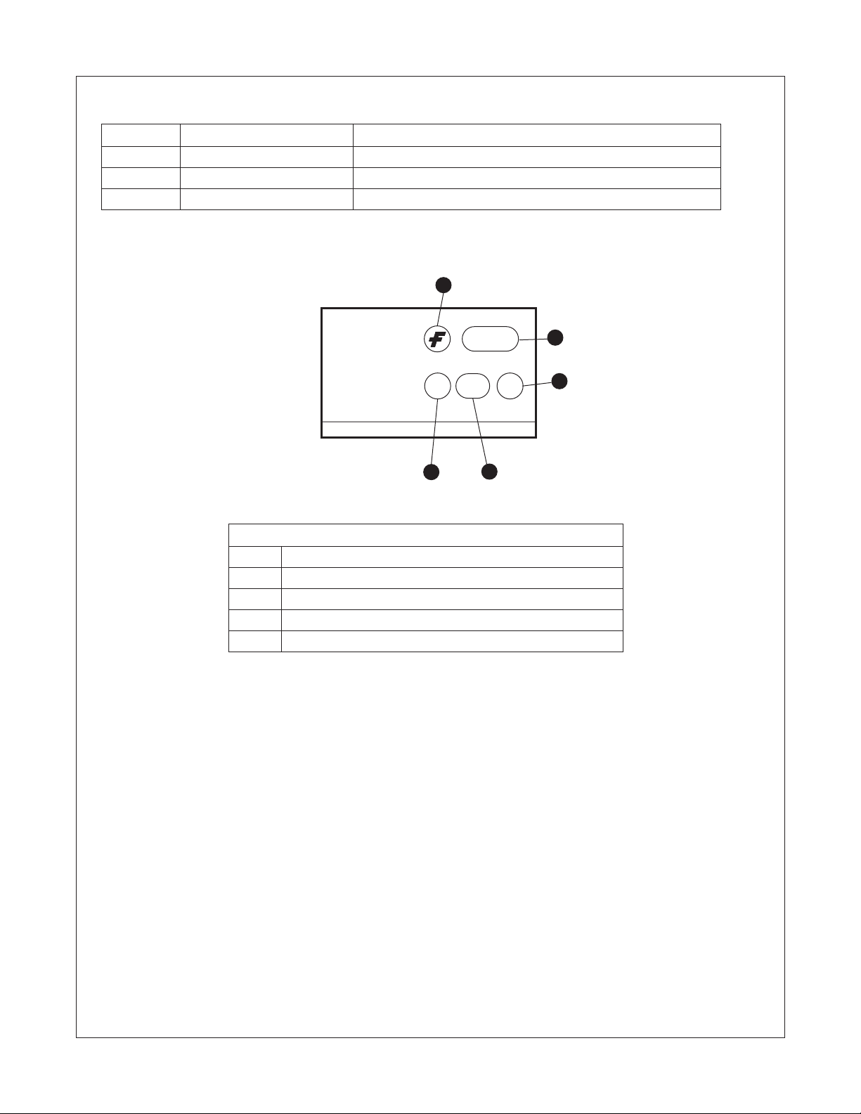
Ordering Information
Option Order Entry Identifier Description
No Suffix HCPL062N Shipped in tubes (50 units per tube)
R1 HCPL062NR1 Tape and Reel (500 units per reel)
R2 HCPL062NR2 Tape and Reel (2500 units per reel)
Marking Information
1
HCPL062N 3.3V Dual Channel High Speed-10 MBit/s Logic Gate Optocouplers
62N
3
Definitions
1Fairchild logo
2Device number
3 One digit year code, e.g., ‘3’
4Two digit work week ranging from ‘01’ to ‘53’
5 Assembly package code
2
SYYX
4
5
HCPL062N Rev. 1.0.0
11 www.fairchildsemi.com
Page 12
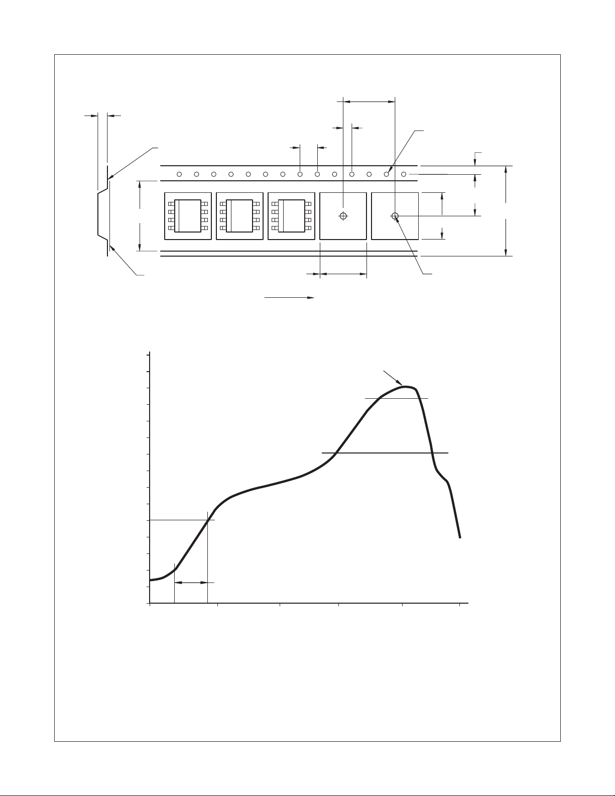
Carrier Tape Specification
3.50 ± 0.20
0.30 MAX
8.3 ± 0.10
4.0 ± 0.10
8.0 ± 0.10
2.0 ± 0.05
HCPL062N 3.3V Dual Channel High Speed-10 MBit/s Logic Gate Optocouplers
Ø1.5 MIN
1.75 ± 0.10
5.5 ± 0.05
12.0 ± 0.3
5.20 ± 0.20
Reflow Profile
300
280
260
240
220
200
180
160
°C
140
120
100
80
60
40
20
0
0.1 MAX
User Direction of Feed
6.40 ± 0.20
260°C
Time above
183°C = 90 Sec
1.822°C/Sec Ramp up rate
33 Sec
0 60 180120 270
Time (s)
Ø1.5 ± 0.1/-0
>245°C = 42 Sec
360
HCPL062N Rev. 1.0.0
12 www.fairchildsemi.com
Page 13

TRADEMARKS
The following are registered and unregistered trademarks Fairchild Semiconductor owns or is authorized to use and is not intended to be an
exhaustive list of all such trademarks.
®
ACEx
Across the board. Around the world.™
ActiveArray™
Bottomless™
Build it Now™
CoolFET™
CROSSVOLT™
CTL™
Current Transfer Logic™
DOME™
2
E
CMOS™
EcoSPARK
®
EnSigna™
FACT Quiet Series™
®
FACT
®
FAST
FASTr™
FPS™
®
FRFET
GlobalOptoisolator™
GTO™
HiSeC™
i-Lo™
ImpliedDisconnect™
IntelliMAX™
ISOPLANAR™
MICROCOUPLER™
MicroPak™
MICROWIRE™
MSX™
MSXPro™
OCX™
OCXPro™
OPTOLOGIC
OPTOPLANAR
®
®
PACMAN™
POP™
Power220
Power247
®
®
PowerEdge™
PowerSaver™
PowerTrench
®
Programmable Active Droop™
®
QFET
QS™
QT Optoelectronics™
Quiet Series™
RapidConfigure™
RapidConnect™
ScalarPump™
SMART START™
®
SPM
STEALTH™
SuperFET™
SuperSOT™-3
SuperSOT™-6
SuperSOT™-8
SyncFET™
TCM™
The Power Franchise
™
®
TinyBoost™
TinyBuck™
TinyLogic
TINYOPTO™
TinyPower™
TinyWire™
TruTranslation™
μSerDes™
UHC
UniFET™
VCX™
Wire™
DISCLAIMER
FAIRCHILD SEMICONDUCTOR RESERVES THE RIGHT TO MAKE CHANGES WITHOUT FURTHER NOTICE TO ANY PRODUCTS
HEREIN TO IMPROVE RELIABILITY, FUNCTION OR DESIGN. FAIRCHILD DOES NOT ASSUME ANY LIABILITY ARISING OUT OF THE
APPLICATION OR USE OF ANY PRODUCT OR CIRCUIT DESCRIBED HEREIN; NEITHER DOES IT CONVEY ANY LICENSE UNDER
ITS PATENT RIGHTS, NOR THE RIGHTS OF OTHERS. THESE SPECIFICATIONS DO NOT EXPAND THE TERMS OF FAIRCHILD’S
WORLDWIDE TERMS AND CONDITIONS, SPECIFICALLY THE WARRANTY THEREIN, WHICH COVERS THESE PRODUCTS.
LIFE SUPPORT POLICY
FAIRCHILD’S PRODUCTS ARE NOT AUTHORIZED FOR USE AS CRITICAL COMPONENTS IN LIFE SUPPORT DEVICES OR
SYSTEMS WITHOUT THE EXPRESS WRITTEN APPROVAL OF FAIRCHILD SEMICONDUCTOR CORPORATION.
As used herein:
1. Life support devices or systems are devices or systems
which, (a) are intended for surgical implant into the body or
(b) support or sustain life, and (c) whose failure to perform
when properly used in accordance with instructions for use
2. A critical component in any component of a life support,
device, or system whose failure to perform can be
reasonably expected to cause the failure of the life support
device or system, or to affect its safety or effectiveness.
provided in the labeling, can be reasonably expected to
result in a significant injury of the user.
PRODUCT STATUS DEFINITIONS
Definition of Terms
Datasheet Identification Product Status Definition
Advance Information Formative or In Design This datasheet contains the design specifications for product
development. Specifications may change in any manner without notice.
Preliminary First Production This datasheet contains preliminary data; supplementary data will be
published at a later date. Fairchild Semiconductor reserves the right to
make changes at any time without notice to improve design.
No Identification Needed Full Production This datasheet contains final specifications. Fairchild Semiconductor
reserves the right to make changes at any time without notice to improve
design.
Obsolete Not In Production This datasheet contains specifications on a product that has been
discontinued by Fairchild Semiconductor. The datasheet is printed for
reference information only.
®
®
Rev. I24
© 2007 Fairchild Semiconductor Corporation www.fairchildsemi.com
 Loading...